US9590838B2 - Transferring data of a dispersed storage network - Google Patents
Transferring data of a dispersed storage network Download PDFInfo
- Publication number
- US9590838B2 US9590838B2 US14/029,347 US201314029347A US9590838B2 US 9590838 B2 US9590838 B2 US 9590838B2 US 201314029347 A US201314029347 A US 201314029347A US 9590838 B2 US9590838 B2 US 9590838B2
- Authority
- US
- United States
- Prior art keywords
- memory
- storage device
- encoded data
- storage
- data slices
- Prior art date
- Legal status (The legal status is an assumption and is not a legal conclusion. Google has not performed a legal analysis and makes no representation as to the accuracy of the status listed.)
- Expired - Fee Related, expires
Links
Images


Classifications
-
- H04L29/08549—
-
- G—PHYSICS
- G06—COMPUTING; CALCULATING OR COUNTING
- G06F—ELECTRIC DIGITAL DATA PROCESSING
- G06F3/00—Input arrangements for transferring data to be processed into a form capable of being handled by the computer; Output arrangements for transferring data from processing unit to output unit, e.g. interface arrangements
- G06F3/06—Digital input from, or digital output to, record carriers, e.g. RAID, emulated record carriers or networked record carriers
- G06F3/0601—Interfaces specially adapted for storage systems
- G06F3/0602—Interfaces specially adapted for storage systems specifically adapted to achieve a particular effect
- G06F3/0614—Improving the reliability of storage systems
-
- G—PHYSICS
- G06—COMPUTING; CALCULATING OR COUNTING
- G06F—ELECTRIC DIGITAL DATA PROCESSING
- G06F12/00—Accessing, addressing or allocating within memory systems or architectures
- G06F12/02—Addressing or allocation; Relocation
-
- G—PHYSICS
- G06—COMPUTING; CALCULATING OR COUNTING
- G06F—ELECTRIC DIGITAL DATA PROCESSING
- G06F3/00—Input arrangements for transferring data to be processed into a form capable of being handled by the computer; Output arrangements for transferring data from processing unit to output unit, e.g. interface arrangements
- G06F3/06—Digital input from, or digital output to, record carriers, e.g. RAID, emulated record carriers or networked record carriers
- G06F3/0601—Interfaces specially adapted for storage systems
- G06F3/0628—Interfaces specially adapted for storage systems making use of a particular technique
- G06F3/0646—Horizontal data movement in storage systems, i.e. moving data in between storage devices or systems
- G06F3/0647—Migration mechanisms
-
- G—PHYSICS
- G06—COMPUTING; CALCULATING OR COUNTING
- G06F—ELECTRIC DIGITAL DATA PROCESSING
- G06F3/00—Input arrangements for transferring data to be processed into a form capable of being handled by the computer; Output arrangements for transferring data from processing unit to output unit, e.g. interface arrangements
- G06F3/06—Digital input from, or digital output to, record carriers, e.g. RAID, emulated record carriers or networked record carriers
- G06F3/0601—Interfaces specially adapted for storage systems
- G06F3/0668—Interfaces specially adapted for storage systems adopting a particular infrastructure
- G06F3/067—Distributed or networked storage systems, e.g. storage area networks [SAN], network attached storage [NAS]
-
- H—ELECTRICITY
- H04—ELECTRIC COMMUNICATION TECHNIQUE
- H04L—TRANSMISSION OF DIGITAL INFORMATION, e.g. TELEGRAPHIC COMMUNICATION
- H04L67/00—Network arrangements or protocols for supporting network services or applications
- H04L67/01—Protocols
- H04L67/10—Protocols in which an application is distributed across nodes in the network
- H04L67/1095—Replication or mirroring of data, e.g. scheduling or transport for data synchronisation between network nodes
-
- H—ELECTRICITY
- H04—ELECTRIC COMMUNICATION TECHNIQUE
- H04L—TRANSMISSION OF DIGITAL INFORMATION, e.g. TELEGRAPHIC COMMUNICATION
- H04L67/00—Network arrangements or protocols for supporting network services or applications
- H04L67/01—Protocols
- H04L67/10—Protocols in which an application is distributed across nodes in the network
- H04L67/1097—Protocols in which an application is distributed across nodes in the network for distributed storage of data in networks, e.g. transport arrangements for network file system [NFS], storage area networks [SAN] or network attached storage [NAS]
-
- H—ELECTRICITY
- H04—ELECTRIC COMMUNICATION TECHNIQUE
- H04L—TRANSMISSION OF DIGITAL INFORMATION, e.g. TELEGRAPHIC COMMUNICATION
- H04L69/00—Network arrangements, protocols or services independent of the application payload and not provided for in the other groups of this subclass
- H04L69/40—Network arrangements, protocols or services independent of the application payload and not provided for in the other groups of this subclass for recovering from a failure of a protocol instance or entity, e.g. service redundancy protocols, protocol state redundancy or protocol service redirection
-
- G—PHYSICS
- G06—COMPUTING; CALCULATING OR COUNTING
- G06F—ELECTRIC DIGITAL DATA PROCESSING
- G06F11/00—Error detection; Error correction; Monitoring
- G06F11/07—Responding to the occurrence of a fault, e.g. fault tolerance
- G06F11/08—Error detection or correction by redundancy in data representation, e.g. by using checking codes
- G06F11/10—Adding special bits or symbols to the coded information, e.g. parity check, casting out 9's or 11's
- G06F11/1076—Parity data used in redundant arrays of independent storages, e.g. in RAID systems
-
- G—PHYSICS
- G06—COMPUTING; CALCULATING OR COUNTING
- G06F—ELECTRIC DIGITAL DATA PROCESSING
- G06F2211/00—Indexing scheme relating to details of data-processing equipment not covered by groups G06F3/00 - G06F13/00
- G06F2211/10—Indexing scheme relating to G06F11/10
- G06F2211/1002—Indexing scheme relating to G06F11/1076
- G06F2211/1057—Parity-multiple bits-RAID6, i.e. RAID 6 implementations
Definitions
- Computers are known to communicate, process, and store data. Such computers range from wireless smart phones to data centers that support millions of web searches, stock trades, or on-line purchases every day.
- a computing system generates data and/or manipulates data from one form into another.
- an image sensor of the computing system generates raw picture data and, using an image compression program (e.g., JPEG, MPEG, etc.), the computing system manipulates the raw picture data into a standardized compressed image.
- an image compression program e.g., JPEG, MPEG, etc.
- computers are capable of processing real time multimedia data for applications ranging from simple voice communications to streaming high definition video.
- general-purpose information appliances are replacing purpose-built communications devices (e.g., a telephone).
- smart phones can support telephony communications but they are also capable of text messaging and accessing the internet to perform functions including email, web browsing, remote applications access, and media communications (e.g., telephony voice, image transfer, music files, video files, real time video streaming. etc.).
- a typical computer storage system includes one or more memory devices aligned with the needs of the various operational aspects of the computer's processing and communication functions.
- the immediacy of access dictates what type of memory device is used.
- random access memory (RAM) memory can be accessed in any random order with a constant response time, thus it is typically used for cache memory and main memory.
- memory device technologies that require physical movement such as magnetic disks, tapes, and optical discs, have a variable response time as the physical movement can take longer than the data transfer, thus they are typically used for secondary memory (e.g., hard drive, backup memory, etc.).
- a computer's storage system will be compliant with one or more computer storage standards that include, but are not limited to, network file system (NFS), flash file system (FFS), disk file system (DFS), small computer system interface (SCSI), internet small computer system interface (iSCSI), file transfer protocol (FTP), and web-based distributed authoring and versioning (WebDAV).
- NFS network file system
- FFS flash file system
- DFS disk file system
- SCSI small computer system interface
- iSCSI internet small computer system interface
- FTP file transfer protocol
- WebDAV web-based distributed authoring and versioning
- memory devices fail; especially commercial grade memory devices that utilize technologies incorporating physical movement (e.g., a disc drive).
- a disc drive it is fairly common for a disc drive to routinely suffer from bit level corruption and to completely fail after three years of use.
- One solution is to utilize a higher-grade disc drive, which adds significant cost to a computer.
- RAID redundant array of independent discs
- a RAID controller adds parity data to the original data before storing it across the array.
- the parity data is calculated from the original data such that the failure of a disc will not result in the loss of the original data.
- RAID 5 uses three discs to protect data from the failure of a single disc.
- RAID 6 can recover from a loss of two discs and requires a minimum of four discs with a storage capacity of n ⁇ 2.
- RAID addresses the memory device failure issue, it is not without its own failure issues that affect its effectiveness, efficiency and security. For instance, as more discs are added to the array, the probability of a disc failure increases, which increases the demand for maintenance. For example, when a disc fails, it needs to be manually replaced before another disc fails and the data stored in the RAID device is lost. To reduce the risk of data loss, data on a RAID device is typically copied on to one or more other RAID devices. While this addresses the loss of data issue, it raises a security issue since multiple copies of data are available, which increases the chances of unauthorized access. Further, as the amount of data being stored grows, the overhead of RAID devices becomes a non-trivial efficiency issue.
- FIG. 1 is a schematic block diagram of an embodiment of a computing system in accordance with the invention.
- FIG. 2 is a schematic block diagram of an embodiment of a computing core in accordance with the invention.
- FIG. 3 is a schematic block diagram of an embodiment of a distributed storage processing unit in accordance with the invention.
- FIG. 4 is a schematic block diagram of an embodiment of a grid module in accordance with the invention.
- FIG. 5 is a diagram of an example embodiment of error coded data slice creation in accordance with the invention.
- FIG. 6A is a schematic block diagram of an embodiment of a dispersed storage (DS) unit in accordance with the invention.
- FIG. 6B is a diagram illustrating an example of free memory availability for a plurality of memories in accordance with the invention.
- FIG. 6C is a diagram illustrating another example of free memory availability for a plurality of memories in accordance with the invention.
- FIG. 6D is a diagram illustrating another example of free memory availability for a plurality of memories in accordance with the invention.
- FIG. 6E is a schematic block diagram of another embodiment of a dispersed storage (DS) unit in accordance with the invention.
- FIG. 6F is a flowchart illustrating an example of migrating encoded data slices in accordance with the invention.
- FIG. 7A is a schematic block diagram of an embodiment of a dispersed storage network (DSN) in accordance with the present invention.
- FIGS. 7B-7D are schematic block diagrams of another embodiment of a dispersed storage network (DSN) illustrating example steps of transferring data in accordance with the present invention
- FIGS. 7E-G are schematic block diagrams of yet another embodiment of a dispersed storage network (DSN) illustrating alternative example steps of transferring data in accordance with the present invention
- FIG. 7H is a flowchart illustrating an example of transferring data in accordance with the present invention.
- FIG. 8 is a flowchart illustrating another example of migrating encoded data slices in accordance with the invention.
- FIG. 9A is a flowchart illustrating an example of utilizing memory in accordance with the invention.
- FIG. 9B is a flowchart illustrating an example of encoding data in accordance with the invention.
- FIG. 9C is a flowchart illustrating an example of decoding encoded data slices in accordance with the invention.
- FIG. 10A is a flowchart illustrating an example of validating a request in accordance with the invention.
- FIG. 10B is a flowchart illustrating an example of producing a request in accordance with the invention.
- FIG. 1 is a schematic block diagram of a computing system 10 that includes one or more of a first type of user devices 12 , one or more of a second type of user devices 14 , at least one distributed storage (DS) processing unit 16 , at least one DS managing unit 18 , at least one storage integrity processing unit 20 , and a distributed storage network (DSN) memory 22 coupled via a network 24 .
- the network 24 may include one or more wireless and/or wire lined communication systems; one or more private intranet systems and/or public internet systems; and/or one or more local area networks (LAN) and/or wide area networks (WAN).
- the DSN memory 22 includes a plurality of distributed storage (DS) units 36 for storing data of the system.
- Each of the DS units 36 includes a processing module and memory and may be located at a geographically different site than the other DS units (e.g., one in Chicago, one in Milwaukee, etc.).
- Each of the user devices 12 - 14 , the DS processing unit 16 , the DS managing unit 18 , and the storage integrity processing unit 20 may be a portable computing device (e.g., a social networking device, a gaming device, a cell phone, a smart phone, a personal digital assistant, a digital music player, a digital video player, a laptop computer, a handheld computer, a video game controller, and/or any other portable device that includes a computing core) and/or a fixed computing device (e.g., a personal computer, a computer server, a cable set-top box, a satellite receiver, a television set, a printer, a fax machine, home entertainment equipment, a video game console, and/or any type of home or office computing equipment).
- a portable or fixed computing device includes a computing core 26 and one or more interfaces 30 , 32 , and/or 33 . An embodiment of the computing core 26 will be described with reference to FIG. 2 .
- each of the interfaces 30 , 32 , and 33 includes software and/or hardware to support one or more communication links via the network 24 indirectly and/or directly.
- interface 30 supports a communication link (wired, wireless, direct, via a LAN, via the network 24 , etc.) between the first type of user device 14 and the DS processing unit 16 .
- DSN interface 32 supports a plurality of communication links via the network 24 between the DSN memory 22 and the DS processing unit 16 , the first type of user device 12 , and/or the storage integrity processing unit 20 .
- interface 33 supports a communication link between the DS managing unit 18 and any one of the other devices and/or units 12 , 14 , 16 , 20 , and/or 22 via the network 24 .
- the system 10 supports three primary functions: distributed network data storage management, distributed data storage and retrieval, and data storage integrity verification.
- data can be distributedly stored in a plurality of physically different locations and subsequently retrieved in a reliable and secure manner regardless of failures of individual storage devices, failures of network equipment, the duration of storage, the amount of data being stored, attempts at hacking the data, etc.
- the DS managing unit 18 performs distributed network data storage management functions, which include establishing distributed data storage parameters, performing network operations, performing network administration, and/or performing network maintenance.
- the DS managing unit 18 establishes the distributed data storage parameters (e.g., allocation of virtual DSN memory space, distributed storage parameters, security parameters, billing information, user profile information, etc.) for one or more of the user devices 12 - 14 (e.g., established for individual devices, established for a user group of devices, established for public access by the user devices, etc.).
- the DS managing unit 18 coordinates the creation of a vault (e.g., a virtual memory block) within the DSN memory 22 for a user device (for a group of devices, or for public access).
- a vault e.g., a virtual memory block
- the DS managing unit 18 also determines the distributed data storage parameters for the vault. In particular, the DS managing unit 18 determines a number of slices (e.g., the number that a data segment of a data file and/or data block is partitioned into for distributed storage) and a read threshold value (e.g., the minimum number of slices required to reconstruct the data segment).
- a number of slices e.g., the number that a data segment of a data file and/or data block is partitioned into for distributed storage
- a read threshold value e.g., the minimum number of slices required to reconstruct the data segment.
- the DS managing unit 18 creates and stores, locally or within the DSN memory 22 , user profile information.
- the user profile information includes one or more of authentication information, permissions, and/or the security parameters.
- the security parameters may include one or more of encryption/decryption scheme, one or more encryption keys, key generation scheme, and data encoding/decoding scheme.
- the DS managing unit 18 creates billing information for a particular user, user group, vault access, public vault access, etc. For instance, the DS managing unit 18 tracks the number of times a user accesses a private vault and/or public vaults, which can be used to generate a per-access bill. In another instance, the DS managing unit 18 tracks the amount of data stored and/or retrieved by a user device and/or a user group, which can be used to generate a per-data-amount bill.
- the DS managing unit 18 also performs network operations, network administration, and/or network maintenance. As at least part of performing the network operations and/or administration, the DS managing unit 18 monitors performance of the devices and/or units of the system 10 for potential failures, determines the devices' and/or units' activation status, determines the devices' and/or units' loading, and any other system level operation that affects the performance level of the system 10 . For example, the DS managing unit 18 receives and aggregates network management alarms, alerts, errors, status information, performance information, and messages from the devices 12 - 14 and/or the units 16 , 20 , 22 . For example, the DS managing unit 18 receives a simple network management protocol (SNMP) message regarding the status of the DS processing unit 16 .
- SNMP simple network management protocol
- the DS managing unit 18 performs the network maintenance by identifying equipment within the system 10 that needs replacing, upgrading, repairing, and/or expanding. For example, the DS managing unit 18 determines that the DSN memory 22 needs more DS units 36 or that one or more of the DS units 36 needs updating.
- the second primary function begins and ends with a user device 12 - 14 .
- a second type of user device 14 has a data file 38 and/or data block 40 to store in the DSN memory 22 , it sends the data file 38 and/or data block 40 to the DS processing unit 16 via its interface 30 .
- a second type of user device 14 has a data file 38 and/or data block 40 to store in the DSN memory 22 , it sends the data file 38 and/or data block 40 to the DS processing unit 16 via its interface 30 .
- the interface 30 functions to mimic a conventional operating system (OS) file system interface (e.g., network file system (NFS), flash file system (FFS), disk file system (DFS), file transfer protocol (FTP), web-based distributed authoring and versioning (WebDAV), etc.) and/or a block memory interface (e.g., small computer system interface (SCSI), internet small computer system interface (iSCSI), etc.).
- OS operating system
- NFS network file system
- FFS flash file system
- DFS disk file system
- FTP file transfer protocol
- WebDAV web-based distributed authoring and versioning
- the interface 30 may attach a user identification code (ID) to the data file 38 and/or data block 40 .
- ID user identification code
- the DS processing unit 16 receives the data file 38 and/or data block 40 via its interface 30 and performs a distributed storage (DS) process 34 thereon (e.g., an error coding dispersal storage function).
- the DS processing 34 begins by partitioning the data file 38 and/or data block 40 into one or more data segments, which is represented as Y data segments.
- the DS processing 34 error encodes (e.g., forward error correction (FEC), information dispersal algorithm, or error correction coding) and slices (or slices then error encodes) the data segment into a plurality of error coded (EC) data slices 42 - 48 , which is represented as X slices per data segment.
- FEC forward error correction
- EC error coded
- n/k For example, if a Reed-Solomon (or other FEC scheme) is used in an n/k system, then a data segment is divided into n slices, where k number of slices is needed to reconstruct the original data (i.e., k is the threshold).
- k is the threshold
- the n/k factor may be 5/3; 6/4; 8/6; 8/5; 16/10.
- the DS processing unit 16 For each EC slice 42 - 48 , the DS processing unit 16 creates a unique slice name and appends it to the corresponding EC slice 42 - 48 .
- the slice name includes universal DSN memory addressing routing information (e.g., virtual memory addresses in the DSN memory 22 ) and user-specific information (e.g., user ID, file name, data block identifier, etc.).
- the DS processing unit 16 transmits the plurality of EC slices 42 - 48 to a plurality of DS units 36 of the DSN memory 22 via the DSN interface 32 and the network 24 .
- the DSN interface 32 formats each of the slices for transmission via the network 24 .
- the DSN interface 32 may utilize an internet protocol (e.g., TCP/IP, etc.) to packetize the EC slices 42 - 48 for transmission via the network 24 .
- an internet protocol e.g., TCP/IP, etc.
- the number of DS units 36 receiving the EC slices 42 - 48 is dependent on the distributed data storage parameters established by the DS managing unit 18 .
- the DS managing unit 18 may indicate that each slice is to be stored in a different DS unit 36 .
- the DS managing unit 18 may indicate that like slice numbers of different data segments are to be stored in the same DS unit 36 .
- the first slice of each of the data segments is to be stored in a first DS unit 36
- the second slice of each of the data segments is to be stored in a second DS unit 36 , etc.
- the data is encoded and distributedly stored at physically diverse locations to improve data storage integrity and security. Further examples of encoding the data segments will be provided with reference to one or more of FIGS. 2-10B .
- Each DS unit 36 that receives an EC slice 42 - 48 for storage translates the virtual DSN memory address of the slice into a local physical address for storage. Accordingly, each DS unit 36 maintains a virtual to physical memory mapping to assist in the storage and retrieval of data.
- the first type of user device 12 performs a similar function to store data in the DSN memory 22 with the exception that it includes the DS processing. As such, the device 12 encodes and slices the data file and/or data block it has to store. The device then transmits the slices 11 to the DSN memory via its DSN interface 32 and the network 24 .
- a second type of user device 14 For a second type of user device 14 to retrieve a data file or data block from memory, it issues a read command via its interface 30 to the DS processing unit 16 .
- the DS processing unit 16 performs the DS processing 34 to identify the DS units 36 storing the slices of the data file and/or data block based on the read command.
- the DS processing unit 16 may also communicate with the DS managing unit 18 to verify that the user device 14 is authorized to access the requested data.
- the DS processing unit 16 issues slice read commands to at least a threshold number of the DS units 36 storing the requested data (e.g., to at least 10 DS units for a 16/10 error coding scheme).
- Each of the DS units 36 receiving the slice read command verifies the command, accesses its virtual to physical memory mapping, retrieves the requested slice, or slices, and transmits it to the DS processing unit 16 .
- the DS processing unit 16 After the DS processing unit 16 has received a read threshold number of slices for a data segment, it performs an error decoding function and de-slicing to reconstruct the data segment. When Y number of data segments has been reconstructed, the DS processing unit 16 provides the data file 38 and/or data block 40 to the user device 14 . Note that the first type of user device 12 performs a similar process to retrieve a data file and/or data block.
- the storage integrity processing unit 20 performs the third primary function of data storage integrity verification.
- the storage integrity processing unit 20 periodically retrieves slices 45 , and/or slice names, of a data file or data block of a user device to verify that one or more slices have not been corrupted or lost (e.g., the DS unit failed).
- the retrieval process mimics the read process previously described.
- the storage integrity processing unit 20 determines that one or more slices is corrupted or lost, it rebuilds the corrupted or lost slice(s) in accordance with the error coding scheme.
- the storage integrity processing unit 20 stores the rebuilt slice, or slices, in the appropriate DS unit(s) 36 in a manner that mimics the write process previously described.
- FIG. 2 is a schematic block diagram of an embodiment of a computing core 26 that includes a processing module 50 , a memory controller 52 , main memory 54 , a video graphics processing unit 55 , an input/output (IO) controller 56 , a peripheral component interconnect (PCI) interface 58 , an IO interface 60 , at least one IO device interface module 62 , a read only memory (ROM) basic input output system (BIOS) 64 , and one or more memory interface modules.
- IO input/output
- PCI peripheral component interconnect
- IO interface 60 at least one IO device interface module 62
- ROM read only memory
- BIOS basic input output system
- the memory interface module(s) includes one or more of a universal serial bus (USB) interface module 66 , a host bus adapter (HBA) interface module 68 , a network interface module 70 , a flash interface module 72 , a hard drive interface module 74 , and a DSN interface module 76 .
- USB universal serial bus
- HBA host bus adapter
- network interface module 70 may function as the interface 30 of the user device 14 of FIG. 1 .
- the IO device interface module 62 and/or the memory interface modules may be collectively or individually referred to as IO ports.
- FIG. 3 is a schematic block diagram of an embodiment of a dispersed storage (DS) processing module 34 of user device 12 and/or of the DS processing unit 16 .
- the DS processing module 34 includes a gateway module 78 , an access module 80 , a grid module 82 , and a storage module 84 .
- the DS processing module 34 may also include an interface 30 and the DSnet interface 32 or the interfaces 68 and/or 70 may be part of user device 12 or of the DS processing unit 16 .
- the DS processing module 34 may further include a bypass/feedback path between the storage module 84 to the gateway module 78 . Note that the modules 78 - 84 of the DS processing module 34 may be in a single unit or distributed across multiple units.
- the gateway module 78 receives an incoming data object that includes a user ID field 86 , an object name field 88 , and the data object field 40 and may also receive corresponding information that includes a process identifier (e.g., an internal process/application ID), metadata, a file system directory, a block number, a transaction message, a user device identity (ID), a data object identifier, a source name, and/or user information.
- the gateway module 78 authenticates the user associated with the data object by verifying the user ID 86 with the DS managing unit 18 and/or another authenticating unit.
- the gateway module 78 obtains user information from the management unit 18 , the user device, and/or the other authenticating unit.
- the user information includes a vault identifier, operational parameters, and user attributes (e.g., user data, billing information, etc.).
- a vault identifier identifies a vault, which is a virtual memory space that maps to a set of DS storage units 36 .
- vault 1 i.e., user 1's DSN memory space
- vault 2 i.e., user 2's DSN memory space
- the operational parameters may include an error coding algorithm, the width n (number of pillars X or slices per segment for this vault), a read threshold T, a write threshold, an encryption algorithm, a slicing parameter, a compression algorithm, an integrity check method, caching settings, parallelism settings, and/or other parameters that may be used to access the DSN memory layer.
- the gateway module 78 uses the user information to assign a source name 35 to the data. For instance, the gateway module 78 determines the source name 35 of the data object 40 based on the vault identifier and the data object. For example, the source name may contain a file identifier (ID), a vault generation number, a reserved field, and a vault identifier (ID). As another example, the gateway module 78 may generate the file ID based on a hash function of the data object 40 . Note that the gateway module 78 may also perform message conversion, protocol conversion, electrical conversion, optical conversion, access control, user identification, user information retrieval, traffic monitoring, statistics generation, configuration, management, and/or source name determination.
- ID file identifier
- ID vault generation number
- ID reserved field
- ID vault identifier
- ID vault identifier
- the gateway module 78 may generate the file ID based on a hash function of the data object 40 . Note that the gateway module 78 may also perform message conversion, protocol conversion, electrical conversion, optical conversion, access control, user
- the access module 80 receives the data object 40 and creates a series of data segments 1 through Y 90 - 92 in accordance with a data storage protocol (e.g., file storage system, a block storage system, and/or an aggregated block storage system).
- segment size is fixed
- the grid module 82 receives the data segments and may manipulate (e.g., compression, encryption, cyclic redundancy check (CRC), etc.) each of the data segments before performing an error coding function of the error coding dispersal storage function to produce a pre-manipulated data segment.
- the grid module 82 error encodes (e.g., Reed-Solomon, Convolution encoding, Trellis encoding, etc.) the data segment or manipulated data segment into X error coded data slices 42 - 44 .
- the value X is chosen as a parameter of the error coding dispersal storage function.
- Other parameters of the error coding dispersal function include a read threshold T, a write threshold W, etc.
- the write threshold W corresponds to a minimum number of DS storage units that acknowledge proper storage of their respective data slices before the DS processing module indicates proper storage of the encoded data segment. Note that the write threshold is greater than or equal to the read threshold for a given number of pillars (X).
- the grid module 82 For each data slice of a data segment, the grid module 82 generates a unique slice name 37 and attaches it thereto.
- the slice name 37 includes a universal routing information field and a vault specific field and may be 48 bytes (e.g., 24 bytes for each of the universal routing information field and the vault specific field).
- the universal routing information field includes a slice index, a vault ID, a vault generation, and a reserved field.
- the slice index is based on the pillar number and the vault ID and, as such, is unique for each pillar (e.g., slices of the same pillar for the same vault for any segment will share the same slice index).
- the vault specific field includes a data name, which includes a file ID and a segment number (e.g., a sequential numbering of data segments 1 -Y of a simple data object or a data block number).
- the grid module may perform post-slice manipulation on the slices. If enabled, the manipulation includes slice level compression, encryption, CRC, addressing, tagging, and/or other manipulation to improve the effectiveness of the computing system.
- the grid module 82 determines which of the DS storage units 36 will store the EC data slices based on a dispersed storage memory mapping associated with the user's vault and/or DS storage unit attributes.
- the DS storage unit attributes may include availability, self-selection, performance history, link speed, link latency, ownership, available DSN memory, domain, cost, a prioritization scheme, a centralized selection message from another source, a lookup table, data ownership, and/or any other factor to optimize the operation of the computing system.
- the number of DS storage units 36 is equal to or greater than the number of pillars (e.g., X) so that no more than one error coded data slice of the same data segment is stored on the same DS storage unit 36 .
- EC data slices of the same pillar number but of different segments e.g., EC data slice 1 of data segment 1 and EC data slice 1 of data segment 2 ) may be stored on the same or different DS storage units 36 .
- the storage module 84 performs an integrity check on the outbound encoded data slices and, when successful, identifies a plurality of DS storage units based on information provided by the grid module 82 .
- the storage module 84 then outputs the encoded data slices 1 through X of each segment 1 through Y to the DS storage units 36 .
- Each of the DS storage units 36 stores its EC data slice(s) and maintains a local virtual DSN address to physical location table to convert the virtual DSN address of the EC data slice(s) into physical storage addresses.
- the user device 12 and/or 14 sends a read request to the DS processing unit 16 , which authenticates the request.
- the DS processing unit 16 sends a read message to each of the DS storage units 36 storing slices of the data object being read.
- the slices are received via the DSnet interface 32 and processed by the storage module 84 , which performs a parity check and provides the slices to the grid module 82 when the parity check was successful.
- the grid module 82 decodes the slices in accordance with the error coding dispersal storage function to reconstruct the data segment.
- the access module 80 reconstructs the data object from the data segments and the gateway module 78 formats the data object for transmission to the user device.
- FIG. 4 is a schematic block diagram of an embodiment of a grid module 82 that includes a control unit 73 , a pre-slice manipulator 75 , an encoder 77 , a slicer 79 , a post-slice manipulator 81 , a pre-slice de-manipulator 83 , a decoder 85 , a de-slicer 87 , and/or a post-slice de-manipulator 89 .
- the control unit 73 may be partially or completely external to the grid module 82 .
- the control unit 73 may be part of the computing core at a remote location, part of a user device, part of the DS managing unit 18 , or distributed amongst one or more DS storage units.
- the pre-slice manipulator 75 receives a data segment 90 - 92 and a write instruction from an authorized user device.
- the pre-slice manipulator 75 determines if pre-manipulation of the data segment 90 - 92 is required and, if so, what type.
- the pre-slice manipulator 75 may make the determination independently or based on instructions from the control unit 73 , where the determination is based on a computing system-wide predetermination, a table lookup, vault parameters associated with the user identification, the type of data, security requirements, available DSN memory, performance requirements, and/or other metadata.
- the pre-slice manipulator 75 manipulates the data segment 90 - 92 in accordance with the type of manipulation.
- the type of manipulation may be compression (e.g., Lempel-Ziv-Welch, Huffman, Golomb, fractal, wavelet, etc.), signatures (e.g., Digital Signature Algorithm (DSA), Elliptic Curve DSA, Secure Hash Algorithm, etc.), watermarking, tagging, encryption (e.g., Data Encryption Standard, Advanced Encryption Standard, etc.), adding metadata (e.g., time/date stamping, user information, file type, etc.), cyclic redundancy check (e.g., CRC32), and/or other data manipulations to produce the pre-manipulated data segment.
- compression e.g., Lempel-Ziv-Welch, Huffman, Golomb, fractal, wavelet, etc.
- signatures e.g., Digital Signature Algorithm (DSA), Ellip
- the encoder 77 encodes the pre-manipulated data segment 92 using a forward error correction (FEC) encoder (and/or other type of erasure coding and/or error coding) to produce an encoded data segment 94 .
- FEC forward error correction
- the encoder 77 determines which forward error correction algorithm to use based on a predetermination associated with the user's vault, a time based algorithm, user direction, DS managing unit direction, control unit direction, as a function of the data type, as a function of the data segment 92 metadata, and/or any other factor to determine algorithm type.
- the forward error correction algorithm may be Golay, Multidimensional parity, Reed-Solomon, Hamming, Bose Ray Chauduri Hocquenghem (BCH), Cauchy-Reed-Solomon, or any other FEC encoder.
- the encoder 77 may use a different encoding algorithm for each data segment 92 , the same encoding algorithm for the data segments 92 of a data object, or a combination thereof.
- the encoded data segment 94 is of greater size than the data segment 92 by the overhead rate of the encoding algorithm by a factor of X/T, where X is the width or number of slices, and T is the read threshold.
- X is the width or number of slices
- T is the read threshold.
- the post-slice manipulator 81 performs, if enabled, post-manipulation on the encoded slices to produce the EC data slices. If enabled, the post-slice manipulator 81 determines the type of post-manipulation, which may be based on a computing system-wide predetermination, parameters in the vault for this user, a table lookup, the user identification, the type of data, security requirements, available DSN memory, performance requirements, control unit directed, and/or other metadata. Note that the type of post-slice manipulation may include slice level compression, signatures, encryption, CRC, addressing, watermarking, tagging, adding metadata, and/or other manipulation to improve the effectiveness of the computing system.
- the post-slice de-manipulator 89 receives at least a read threshold number of EC data slices and performs the inverse function of the post-slice manipulator 81 to produce a plurality of encoded slices.
- the de-slicer 87 de-slices the encoded slices to produce an encoded data segment 94 .
- the decoder 85 performs the inverse function of the encoder 77 to recapture the data segment 90 - 92 .
- the pre-slice de-manipulator 83 performs the inverse function of the pre-slice manipulator 75 to recapture the data segment 90 - 92 .
- FIG. 5 is a diagram of an example of slicing an encoded data segment 94 by the slicer 79 .
- the encoded data segment 94 includes thirty-two bits, but may include more or less bits.
- the slicer 79 disperses the bits of the encoded data segment 94 across the EC data slices in a pattern as shown. As such, each EC data slice does not include consecutive bits of the data segment 94 reducing the impact of consecutive bit failures on data recovery.
- EC data slice 2 which includes bits 1 , 5 , 9 , 13 , 17 , 25 , and 29 ) is unavailable (e.g., lost, inaccessible, or corrupted)
- the data segment can be reconstructed from the other EC data slices (e.g., 1, 3 and 4 for a read threshold of 3 and a width of 4).
- FIG. 6A is a schematic block diagram of an embodiment of a dispersed storage (DS) unit 36 .
- the DS unit 36 includes a dispersed storage network (DSN) interface 32 , a control module 104 , a configuration memory 102 , and a plurality of memories A-E.
- the control module may be implemented as logic in a computing core 26 and/or as a software algorithm operating on a computing core 26 .
- a processing module of the control module may execute a method to control the plurality of memories A-E, stored encoded data slices in the plurality of memories A-E, retrieve encoded data slices from the plurality of memories, and utilize the configuration memory as a repository for configuration information (e.g., virtual DSN addressing range assignments for each of the memories) associated with the DS unit.
- the configuration memory 102 and each memory of the plurality of memories A-E may be a read-only memory, random access memory, volatile memory, non-volatile memory, static memory, dynamic memory, flash memory, magnetic disk drive memory, solid state memory, cache memory, and/or any device that stores digital information.
- the configuration memory 102 is implemented utilizing a solid-state flash memory and each of the plurality of memories A-E are implemented utilizing a magnetic disk drive memory.
- the control module 104 receives a virtual DSN address range assignment message that includes an overall address range assignment for the DS unit 36 .
- the control module 104 determines available memories as memories A-E based on one or more of configuration information retrieved from the configuration memory 102 , an installation indicator, a query, and a message.
- the control module 104 determines subdivisions of the address range to assign to each of the plurality of memories A-E. For instance, the control module assigns address range 101 - 200 to memory A, address range 201 - 300 to memory B, address range 301 - 400 to memory C, address range 401 - 500 to memory D, and address range 501 - 600 to memory A when the overall address range assignment is 101-600.
- contiguous address ranges are assigned to the plurality of memories such that there are no gaps in address ranges.
- each memory is assigned a uniform number of addresses within an address range assignment when an expected address range utilization is of a uniform nature.
- the control module 104 assigns non-uniform address ranges to each of the memories A-E when the expected address range utilization is of a non-uniform nature.
- the control module 104 stores address range assignment information as configuration information in the configuration memory 102 (e.g., address range assignments by memory).
- the control module 104 receives a storage request via the DSN interface 32 , wherein the request includes an encoded data slice and slice name.
- the control module 104 retrieves configuration information from the configuration memory 102 .
- the control module 104 determines an assigned memory based on the slice name and the configuration information such that the slice name address falls within an address range associated with the assigned memory.
- the control module 104 stores the encoded data slice in the assigned memory and updates the configuration information with the slice name.
- a memory of the plurality of memories A-E may be utilized to store more data slices than other memories when the slice names of successive storage requests fall within an address range associated with the memory. Note that an amount of available free space of each of the memories may vary over time.
- a memory utilization balancing method is discussed in greater detail with reference to FIGS. 6B-6F .
- FIG. 6B is a diagram illustrating an example of free memory (e.g., available memory) availability for a plurality of memories.
- the plurality of memories A-E may be implemented in a single dispersed storage (DS) unit.
- the plurality of memories A-E may be implemented in two or more DS units.
- memory A is 60% free (e.g., not utilized)
- memory B is 50% free
- memory C is 30% free
- memory D is 45% free
- memory E is 40% free.
- memory C may have been utilized more often than other memories for data storage operations as memory C has a least amount of free space.
- a memory pair may be selected for migration when an associated migration score is the highest of each migration score of the consecutive memory pairs.
- encoded data slices may be moved from a memory with the least amount of free space of the memory pair to the other memory of the memory pair. For instance, encoded data slices may be moved from memory C to memory B to balance the memory utilization.
- a configuration information update may indicate updated virtual dispersed storage network (DSN) address range assignments for the rebalanced memories such that the slice names of the encoded data slices that are associated with corresponding memories (e.g., where they are stored).
- DSN virtual dispersed storage network
- FIG. 6C is a diagram illustrating another example of free memory availability for a plurality of memories subsequent to an encoded data slice migration as previously discussed with reference to FIG. 6B .
- memory A is 60% free memory B is 40% free, memory C is 40% free, memory D is 45% free, and memory E is 40% free.
- memory B and memory C have 40% free as a result of rebalancing such a memory pair.
- the example continues such that a migration score may be calculated for each consecutive memory pair of the plurality of memories.
- the memory pair of memory A and memory B is selected for rebalancing based on the migration score of 0.5 being greater than a migration threshold when the migration threshold is 0.4.
- encoded data slices are migrated from a memory with the least amount of free space of the memory pair to the other memory of the memory pair. For instance, encoded data slices are moved from memory B to memory A to balance the memory utilization.
- a configuration information update indicates updated virtual dispersed storage network (DSN) address range assignments for the rebalanced memories such that the slice names of the encoded data slices that are associated with corresponding memories (e.g., where they are stored).
- DSN virtual dispersed storage network
- FIG. 6D is a diagram illustrating another example of free memory availability for a plurality of memories subsequent to an encoded data slice migration as previously discussed with reference to FIG. 6C .
- memory A is 50% free memory B is 50% free, memory C is 40% free, memory D is 45% free, and memory E is 40% free.
- memory A and memory B have 50% free as a result of rebalancing such a memory pair.
- the example continues such that a migration score may be calculated for each consecutive memory pair of the plurality of memories (e.g., as previously discussed).
- the memory pair of memory B and memory C is chosen for rebalancing based on the migration score of 0.25 being greater than a migration threshold when the migration threshold is 0.2.
- encoded data slices are migrated from a memory with the least amount of free space of the memory pair to the other memory of the memory pair. For instance, encoded data slices are migrated from memory B to memory C to balance the memory utilization.
- a configuration information update indicates updated virtual dispersed storage network (DSN) address range assignments for the rebalanced memories such that the slice names of the encoded data slices that are associated with corresponding memories (e.g., where they are stored).
- DSN virtual dispersed storage network
- FIG. 6E is a schematic block diagram of another embodiment of a dispersed storage (DS) unit.
- the DS unit 36 includes a dispersed storage network (DSN) interface 32 , a control module 104 , a configuration memory 102 , and a plurality of memory devices A-E.
- the control module 104 includes a selector 106 to route a selected encoded data slice from a plurality of received encoded data slices to a selected memory of the memories A-E.
- the selected slice may be routed to the selected memory in accordance with at least one of a slice name addressing approach and a quantity load balancing function.
- the control module 104 determines the selected memory based on a slice name associated with the encoded data slice when the slice name addressing approach is utilized.
- the control module 104 stores a plurality of encoded data slices in the plurality of memory devices A-E of a dispersed storage (DS) unit of a dispersed storage network (DSN) memory using the quantity load balancing function when the quantity load balancing function is utilized.
- the control module 104 stores the plurality of encoded data slices in the plurality of memory devices A-E using the quantity load balancing function to substantially balance a quantity of encoded data slices stored within each of the plurality of memory devices, wherein data size of at least some of the plurality of encoded data slices is different.
- the quantity load balancing includes at least one of a round robin even distribution approach by quantity of encoded data slices, an uneven distribution approach by quantity of encoded data slices (e.g., 2 slices to memory A for every 1 slice to memories B-E), and a skipping distribution approach by quantity of encoded data slices (e.g., 1 slice to memory A, no slices to memory B, and 1 slice to memories C-E).
- the DSN interface 32 receives encoded data slices 1 - 10 .
- the DSN interface 32 forwards the encoded data slices 1 - 10 to the control module 104 .
- the control module 104 determines the quantity load balancing function to include the round robin scheme of storage of the encoded data slices 1 - 10 evenly amongst the plurality of memory devices A-E based on a predetermination.
- the control module 104 controls the selector 106 to route the encoded data slice 1 to memory A, encoded data slice 2 to memory B, encoded data slice 3 to memory C, encoded data slice 4 to memory D, encoded data slice 5 to memory E, encoded data slice 6 to memory A, encoded data slice 7 to memory B, encoded data slice 8 to memory C, encoded data slice 9 to memory D, and encoded data slice 10 to memory E.
- FIG. 6F is a flowchart illustrating an example of migrating encoded data slices.
- the method begins with step 110 where a processing module (e.g., of a dispersed storage (DS) unit) stores a plurality of encoded data slices in a plurality of memory devices of a dispersed storage (DS) unit of a dispersed storage network (DSN) memory using a quantity load balancing function to substantially balance a quantity of encoded data slices stored within each of the plurality of memory devices, wherein data size of at least some of the plurality of encoded data slices is different.
- a processing module e.g., of a dispersed storage (DS) unit
- DSN dispersed storage network
- the method continues at step 112 where the processing module determines whether an available memory imbalance exists between a first memory device of the plurality of memory devices and a second memory device of the plurality of memory devices.
- the determining whether the available memory imbalance exists includes determining an available memory value of the first memory device, determining an available memory value of the second memory device, determining a difference available memory value based on the available memory values of the first and second memory device, comparing the difference available memory value with an available memory differential threshold, and when the comparing the difference available memory value with the available memory differential threshold is unfavorable, indicating that the available memory imbalance exists.
- the available memory differential threshold may be very low such that any difference triggers a migration.
- the determining the difference available memory value includes at least one of subtracting the available memory value of the first memory device from the available memory value of the second memory device to produce the difference available memory value and calculating a migration score based on a subtraction of the available memory value of the first memory device from the available memory value of the second memory device to produce an available memory resultant value and dividing the available memory resultant value from one of the available memory value of the first memory device and the available memory value of the second memory device.
- the method continues at step 114 , when the available memory imbalance exists, where the processing module migrates one or more encoded data slices between the first and second memory devices to reduce the available memory imbalance.
- the migrating the one or more encoded data slices between the first and second memory devices includes, when the available memory imbalance exists because an available memory value of the first memory device is less than an available memory value of the second memory device, selecting the one or more encoded data slices associated with the first memory for migration to produce a migration set of encoded data slices, retrieving the migration set of encoded data slices from the first memory, storing the migration set of encoded data slices in the second memory, modifying a first set of DSN addresses associated with the first memory device to produce a modified first set of DSN addresses, and modifying a second set of DSN addresses associated with the second memory device to produce a modified second set of DSN addresses.
- the selecting the one or more encoded data slices includes determining a magnitude of the available memory imbalance, determining data size of the one or more encoded data slices, and selecting the one or more encoded data slices based on the magnitude of the available memory imbalance and the data size of the one or more encoded data slices.
- the selecting the one or more encoded data slices includes at least one of identifying encoded data slices based on an encoded data slice priority level and identifying encoded data slices based on an encoded data slice type indicator.
- the method continues at step 116 where the processing module updates a slice location table based on the migrating the one or more encoded data slices between the first and second memory devices.
- the modifying the first set of DSN addresses to produce the modified first set of DSN addresses includes modifying the first set of DSN addresses to exclude DSN addresses associated with the migration set of encoded data slices.
- the modifying the second set of DSN addresses to produce the modified second set of DSN addresses includes modifying the second set of DSN addresses to include DSN addresses associated with the migration set of encoded data slices.
- the method continues at step 118 where the processing module determines whether a second available memory imbalance exists between a third memory device of the plurality of memory devices and a fourth memory device of the plurality of memory devices.
- the method continues at step 120 , when the second available memory imbalance exists, where the processing module migrates another one or more encoded data slices between the third and fourth memory devices to reduce the available memory imbalance.
- step 122 the processing module compares the available memory imbalance with the second available memory imbalance and prioritizes the migrating of the one or more encoded data slices between the first and second memory devices and the migrating of the other one or more encoded data slices between the third and fourth memory devices based on the comparing. For example, the processing module prioritizes migrating the other one or more encoded data slices between the third and fourth memory devices when the second available memory imbalance includes an imbalance that is greater than the imbalance of the available memory imbalance. Alternatively, processing module considers imbalances of all possible pairings of memory devices to prioritize encoded data slice migration.
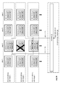
- FIG. 7A is a schematic block diagram of an embodiment of a dispersed storage network (DSN) that includes a DSN memory implemented at four sites, the network 24 and the dispersed storage (DS) processing unit 16 of FIG. 1 .
- the DS processing unit 16 includes the DS processing module 34 of FIG. 1 .
- the DS processing module 34 may include further modules.
- the DS processing module 34 provides a first module and a second module.
- the DSN memory implementation at each of the four sites includes a plurality of storage devices.
- Each storage device may be implemented utilizing one or more of a memory, a memory array, a disk drive, a solid-state drive, an optical disk drive, a magnetic disk drive, a storage unit, a DS unit, a distributed storage and task (DST) execution unit, and a storage server.
- a first storage device includes DS unit 4 _ 1 at the fourth site and a second storage device includes DS unit 4 _ 2 at the fourth site.
- the first storage device includes a first memory 4 _ 1 _ 1 within the DS unit 4 _ 1 and the second storage device includes a second memory 4 _ 1 _ 2 within the DS unit 4 _ 1 .
- the DSN memory has a logical address range (e.g., DSN address range of slice names), where each of each site is assigned a logical address sub-range of the logical address range and each of the plurality of storage devices is assigned a unique fraction of a corresponding logical address sub-range in a storage device sequential manner (e.g., contiguous addressing from storage device to storage device of a common site).
- a logical address range e.g., DSN address range of slice names
- a first set of DS units 1 _ 1 , 2 _ 1 , 3 _ 1 , and 4 _ 1 are associated with a first part of the logical address range and a second set of DS units 1 _ 2 , 2 _ 2 , 3 _ 2 , and 4 _ 2 are associated with a second part of the logical address range, where each DS unit is assigned a corresponding unique fraction of a corresponding logical address sub-range of an associated site.
- the first module when operable within the DS processing unit 16 , causes the DS processing module 34 to detect unavailability of a storage device of a site of the DSN memory to produce an unavailable storage device.
- the DS processing unit 16 receives an error message associated with memory 2 _ 1 _ 2 of DS unit 2 _ 1 (e.g., or any one or more memory devices) indicating the unavailability of the storage device.
- the DS processing unit 16 receives an error message associated with DS unit 3 _ 2 indicating the unavailability of the storage device (e.g., unavailability of the entire DS unit (i.e., DS unit off-line), unavailability of one or more memory devices of a plurality of memory devices associated with the DS unit).
- the unavailability of the storage device e.g., unavailability of the entire DS unit (i.e., DS unit off-line), unavailability of one or more memory devices of a plurality of memory devices associated with the DS unit.
- the second module when operable within the DS processing unit 16 , causes the DS processing module 34 to reassign, within the site, a fraction of a logical address sub-range of the unavailable storage device to one or more other storage devices of the plurality of storage devices of the site while maintaining a storage device sequential manner of allocating fractions of the logical address sub-range (e.g., issues address assignment messages, updates logical address-to-storage device tables).
- the DS processing unit 16 rebuilds one or more logically addressable data objects (e.g., encoded data slices associated with slice names of the logical addressing stored in the unavailable storage device) to produce one or more rebuilt data objects (e.g., rebuilt encoded data slices).
- the DS processing module 34 retrieves a decode threshold number of slices 11 for each set of slices from other storage devices of a set of storage devices that includes the unavailable storage device, where the set of storage devices shares a common portion of the DSN memory logical address range.
- the DS processing module 34 decodes each decode threshold number of slices 11 to reproduce the one or more rebuilt data objects as the rebuilt encoded data slices.
- the DS processing unit 16 stores the one or more rebuilt data objects in the one or more other storage devices.
- the DS processing module 34 stores a first portion of the rebuilt encoded data slices in memory 2 _ 1 _ 1 and a second portion of the rebuilt encoded data slices in memory 2 _ 1 _ 3 of DS unit 2 _ 1 when the unavailable storage device is memory 2 _ 1 _ 2 .
- the DS processing module stores the first portion of the rebuilt encoded data slices in DS unit 3 _ 1 and the second portion of the rebuilt encoded data slices in DS unit 3 _ 3 when the unavailable storage device is DS unit 3 _ 2 .
- the DS processing unit 16 When the unavailable storage device becomes available (e.g., receive an availability indicator), the DS processing unit 16 reallocates the fraction of the logical address sub-range from the one or more other storage devices to the storage device (e.g., issues address assignment messages, updates the logical address-to-storage device tables). With the reallocation, the DS processing unit 16 transfers the one or more rebuilt data objects from the one or more other storage devices to the storage device. As a specific example, the DS processing module 34 retrieves the rebuilt encoded data slices from the one or more other storage devices and stores the retrieved rebuilt encoded data slices in the storage device. As another specific example, the DS processing module 34 issues a write commands to the one or more other storage devices to transfer the rebuilt encoded data slices to the storage device.
- FIGS. 7B-7G discuss the detecting, the rebuilding, and the transferring when the storage devices are implemented as the DS units while FIGS. 7E-G discuss the detecting, the rebuilding, and the transferring when the storage devices are implemented as the memories.
- FIGS. 7B-7D are schematic block diagrams of another embodiment of a dispersed storage network (DSN) illustrating example steps of transferring data.
- the DSN includes a dispersed storage (DS) processing module 34 and pluralities of storage devices implemented at a plurality of sites.
- the DS processing module 34 includes one or more of the decoder 85 and the encoder 77 of FIG. 4 .
- the other embodiment of the DSN further includes the example of FIG. 7A when the storage device is implemented as the dispersed storage (DS) unit.
- each site includes a plurality of DS units where logically addressable data objects are stored in the storage device sequential manner of allocating the fractions of the logical address sub-range.
- the set of DS units 1 _ 1 , 2 _ 1 , 3 _ 1 , and 4 _ 1 are associated with a slice set address range 1
- the set of DS units 1 _ 2 , 2 _ 2 , 3 _ 2 , and 4 _ 2 are associated with a slice set address range 2 , etc.
- the slice set address range 1 is adjacent and sequential with the slice set address range 2 etc.
- the DS processing module 34 rebuilds the one or more logically addressable data objects to produce one or more rebuilt data objects.
- the DS processing module 34 sends rebuilding requests to other sites regarding the one or more logically addressable data objects. For instance, the DS processing module 34 issues read slice requests to DS units 1 _ 2 , 2 _ 2 , and 4 _ 2 to retrieve slices 1 - 2 , 2 - 2 , and 4 - 2 that are associated with the common slice set address range 2 of slices 3 - 2 associated with the unavailable storage device DS unit 3 _ 2 . As another instance, the DS processing module 34 issues partial slice requests to the DS units 1 _ 2 , 2 _ 2 , and 4 _ 2 to receive partially encoded slices with respect to slices 3 - 2 to be rebuilt.
- a DS unit generates a partially encoded slice by a series of steps.
- an encoding matrix is obtained that was utilized to generate a slice to be rebuilt.
- the encoding matrix is reduced to produce a square matrix that exclusively includes rows associated with the decode threshold number of partial encoded slices (e.g., DS units 1 _ 2 , 2 _ 2 , and 4 _ 2 ).
- the square matrix is inverted to produce an inverted matrix.
- the inverted matrix is matrix multiplied with a slice associated with the DS unit to produce a vector.
- the vector is matrix multiplied by a row of the encoding matrix corresponding to the slice to be rebuilt to produce the partially slice.
- FIG. 7C illustrates a continuation of the example of transferring data.
- the DS processing module 34 reassigns, within the site, the fraction of the logical address sub-range of the unavailable storage device to one or more other storage devices of the plurality of storage device while maintaining the storage device sequential manner of allocating the fractions of the logical address sub-range.
- the DS processing module 34 divides the fraction of the logical address sub-range into a first portion and a second portion (e.g., slices 3 - 2 - a and slices 3 - 2 - b ).
- the DS processing module 34 reassigns the first portion to one of the one or more other storage devices having a first contiguous fraction of the logical address sub-range.
- the DS processing module 34 reassigns slices 3 - 2 - a to DS unit 3 _ 1 such that DS unit 3 _ 1 now covers slice set address range 1 and the first portion of the slice set address range 2 with regards to addresses of the third site.
- the DS processing module 34 reassigns the second portion (e.g., slices 3 - 2 - b ) to a second one of the one or more other storage devices (e.g., DS unit 3 _ 3 ) having a second contiguous fraction of the logical address sub-range.
- the DS processing module 34 completes rebuilding the one or more logically addressable data objects (e.g., slices 3 - 2 ) from the rebuilding data.
- encoder 77 encodes segments 2 using the dispersed storage error coding function to produce the slices 3 - 2 - a and the slices 3 - 2 - b . Having rebuilt the data objects, the DS processing module 34 stores the one or more rebuilt data objects in the one or more other storage devices.
- the encoder 77 facilitates storage of slices 3 - 2 - a in DS unit 3 _ 1 and facilitates storage of slices 3 - 2 - b in DS unit 3 _ 3 .
- the facilitating includes sending one or more write requests to the one or more other storage devices regarding the one or more rebuilt data objects.
- a write request of the one or more write requests includes a logical address within the reassigned fraction of the logical address sub-range and a corresponding one of the one or more rebuilt data objects.
- FIG. 7D illustrates a continuation of the example of transferring data.
- the DS processing module 34 detects that the unavailable storage device is available. As a specific example, the DS processing module 34 receives a status 3 _ 2 from DS unit 3 _ 2 indicating that a repair or replacement of the unavailable storage device has been completed. As another specific example, the DS processing module 34 receives the status 3 _ 2 from DS unit 3 _ 2 indicating that the unavailable storage device is coming back on-line. As yet another specific example, the DS processing module 34 receives the status 3 _ 2 from DS unit 3 _ 2 indicating that a repair or replacement of a memory device within the storage device has been completed.
- the DS processing module 34 When the DS processing module 34 detects that the unavailable storage device becomes available, the DS processing module 34 reallocates the fraction of the logical address sub-range from the one or more other storage devices to the storage device. For example, the DS processing module 34 issues a logical address assignment message to each of the DS units 3 _ 1 , 3 _ 2 , and 3 _ 3 indicating that DS unit 3 _ 1 is now associated with slice set address range 1 , a DS unit 3 _ 2 is now associated with slice set address range 2 , and DS unit 3 _ 3 is now associated with slice set address range 3 .
- a first set of memories 1 _ 1 _ 1 , 2 _ 1 _ 1 , 3 _ 1 _ 1 , and 4 _ 1 _ 1 are associated with a slice set address sub-range 1
- a second set of memories 1 _ 1 _ 2 , 2 _ 1 _ 2 , 3 _ 1 _ 2 , and 4 _ 1 _ 2 are associated with a slice set address sub-range 2 , etc.
- the slice set address sub-range 1 is adjacent and sequential with the slice set address sub-range 2 etc.
- the DS processing module 34 issues read slice requests to memories 1 _ 1 _ 2 , 3 _ 1 _ 2 , and 4 _ 1 _ 2 to retrieve sets of slices 1 - 2 A, 3 - 2 A, and 4 - 2 A and sets of slices 1 - 2 B, 3 - 2 B, and 4 - 2 B that are associated with the common slice set address sub-range 2 of slices 2 - 2 A, 2 - 2 B associated with the unavailable storage device (e.g., memory 2 _ 1 _ 2 ).
- the unavailable storage device e.g., memory 2 _ 1 _ 2 .
- the DS processing module 34 issues partial slice requests to the memories 1 _ 1 _ 2 , 3 _ 1 _ 2 , and 4 _ 1 _ 2 to receive partially encoded slices with respect to slices 2 - 2 A, 2 - 2 B to be rebuilt.
- the decoder 85 receives, in response to the rebuilding requests, rebuilding data (e.g., a decode threshold number of slices or partially encoded slices).
- the decoder 85 decodes the rebuilding data to rebuild the one or more logically addressable data objects. For example, the decoder 85 decodes the decode threshold number of slices per set of slices 1 - 2 A, 3 - 2 A, and 4 - 2 A using a dispersed storage error coding function to produce rebuilt segments 2 A.
- the decoder 85 applies modulo addition (e.g., exclusive OR) to the decode threshold number of partial encoded slices two produce the rebuilt segments.
- modulo addition e.g., exclusive OR
- FIG. 7F illustrates a continuation of the alternative example of transferring data.
- the DS processing module 34 reassigns, within the site, the fraction of the logical address sub-range of the unavailable storage device to one or more other storage devices of the plurality of storage device while maintaining the storage device sequential manner of allocating the fractions of the logical address sub-range.
- the DS processing module 34 divides the fraction of the logical address sub-range into a first portion and a second portion (e.g., slices 2 - 2 A and slices 2 - 2 B).
- the DS processing module 34 reassigns the first portion to one of the one or more other storage devices having a first contiguous fraction of the logical address sub-range.
- the DS processing module 34 reassigns slices 2 - 2 A to memory 2 _ 1 _ 1 such that memory 2 _ 1 _ 1 now covers slice set address sub-range 1 and the first portion of the slice set address sub-range 2 with regards to addresses of the second site.
- the DS processing module 34 reassigns the second portion (e.g., slices 2 - 2 B) to a second one of the one or more other storage devices (e.g., memory 2 _ 1 _ 3 ) having a second contiguous fraction of the logical address sub-range.
- the facilitating includes sending one or more write requests to the one or more other storage devices regarding the one or more rebuilt data objects.
- a write request of the one or more write requests includes a logical address within the reassigned fraction of the logical address sub-range and a corresponding one of the one or more rebuilt data objects.
- FIG. 7G illustrates a continuation of the alternative example of transferring data.
- the DS processing module 34 detects that the unavailable storage device is available. As a specific example, the DS processing module 34 receives a status 2 _ 1 _ 2 from DS unit 2 _ 1 indicating that a repair or replacement of the memory device 2 _ 1 _ 2 has been completed. As another specific example, the DS processing module 34 receives the status 2 _ 1 _ 2 from DS unit 2 _ 1 indicating that the unavailable storage device is coming back on-line.
- the DS processing module 34 When the DS processing module 34 detects that the unavailable storage device becomes available, the DS processing module 34 reallocates the fraction of the logical address sub-range from the one or more other storage devices to the storage device. For example, the DS processing module 34 issues a logical address assignment message to DS units 2 _ 1 indicating that memory 2 _ 1 _ 1 is now associated with slice set address sub-range 1 , memory 2 _ 1 _ 2 is now associated with slice set address sub-range 2 , and memory 2 _ 1 _ 3 is now associated with slice set address sub-range 3 .
- the DS processing module 34 transfers the one or more rebuilt data objects from the one or more other storage devices to the storage device.
- the DS processing module 34 issues one or more write commands to the one or more other storage devices to write the one or more rebuilt data objects to the storage device.
- the DS processing module 34 issues a write command (e.g., transfer slice request) to DS unit 2 _ 1 to transfer slices 2 - 2 A from memory 2 _ 1 _ 1 to memory 2 _ 1 _ 2 and the DS processing module 34 issues a write command to DS unit 2 _ 1 to transfer slices 2 - 2 B from memory 2 _ 1 _ 3 to memory 2 _ 1 _ 2 .
- a write command e.g., transfer slice request
- the DS processing module 34 receives an acknowledge of successful storage of the one or more rebuilt data objects by the storage device (e.g., one or more favorable write slice responses).
- the DS processing module 34 issues a delete command to the one or more other storage devices to delete the one or more rebuilt data objects.
- the DS processing module 34 issues write slice requests to DS unit 2 _ 1 indicating to delete slices 2 - 2 A from memory 2 _ 1 _ 1 and to delete slices 2 - 2 B from memory 2 _ 1 _ 3 .
- FIG. 7H is a flowchart illustrating an example of transferring data.
- the method begins at step 124 where a processing module (e.g., of a dispersed storage (DS) processing unit of a dispersed storage network (DSN)) detects unavailability of a storage device of a site of DSN memory to produce an unavailable storage device.
- the DSN memory includes a plurality of sites that includes the site.
- the site includes a plurality of storage devices that includes the storage device.
- the DSN memory has a logical address range, where the site is assigned a logical address sub-range of the logical address range and each of the plurality of storage devices is assigned a fraction of the logical address sub-range in a storage device sequential manner.
- the processing module detects unavailability of one or more memory devices of a plurality of memory devices associated with the storage device (e.g., receive an error message associated with the one or more memory devices).
- the processing module detects that the storage device is off-line (e.g., no responses are received within a response timeframe subsequent to issuing a request to the storage device).
- the method continues at step 126 where the processing module reassigns, within the site, the fraction of the logical address sub-range of the unavailable storage device to one or more other storage devices of the plurality of storage device while maintaining the storage device sequential manner of allocating the fractions of the logical address sub-range.
- the processing module reassigns, within the site, the fraction of the logical address sub-range of the unavailable storage device to one or more other storage devices of the plurality of storage device while maintaining the storage device sequential manner of allocating the fractions of the logical address sub-range.
- the processing module divides the fraction of the logical address sub-range into a first portion and a second portion (e.g., evenly), reassigns the first portion to one of the one or more other storage devices having a first contiguous fraction of the logical address sub-range, and reassigns the second portion to a second one of the one or more other storage devices having a second contiguous fraction of the logical address sub-range.
- the reassigning includes at least one of issuing a reassignment message to the one or more other storage devices, where the reassignment message includes an indication of the first and second portions, and updating a system DSN memory logical address range assignment table.
- step 128 the processing module rebuilds the one or more logically addressable data objects to produce one or more rebuilt data objects.
- the processing module sends rebuilding requests to other sites regarding the one or more logically addressable data objects. For instance, the processing module issues read slice requests to a decode threshold number of storage devices of a set of storage devices that includes the unavailable storage device.
- the processing module receives, in response to the rebuilding requests, rebuilding data. For instance, the processing module receives a decode threshold number of encoded data slices for each set of encoded data slices that includes an encoded data slice as one of the one or more logically addressable data objects.
- the processing module Having received the rebuilding data, the processing module rebuilds the one or more logically addressable data objects from the rebuilding data. For instance, the processing module decodes the decode threshold number of encoded data slices using a dispersed storage error coding function to reproduce a data segment. Next, the processing module encodes the data segment using the dispersed storage error coding function to reproduce a rebuilt encoded data slice associated with the unavailable storage device.
- step 130 the processing module stores the one or more rebuilt data objects in the one or more other storage devices.
- the processing module sends one or more write requests to the one or more other storage devices regarding the one or more rebuilt data objects, where a write request of the one or more write requests includes a logical address within the reassigned fraction of the logical address sub-range and a corresponding one of the one or more rebuilt data objects.
- the processing module sends a write slice request that includes the rebuilt encoded data slice to another storage device that has been reassigned a fraction of the logical address sub-range that corresponds to the rebuilt encoded data slice.
- the method continues at step 134 where the processing module re-allocates the fraction of the logical address sub-range from the one or more other storage devices to the storage device (e.g., issuing reassignment messages, updating the system DSN memory logical address range assignment table).
- the method continues at step 136 where the processing module transfers the one or more rebuilt data objects from the one or more other storage devices to the storage device.
- the processing module issues one or more write commands (e.g., a transfer instruction message) to the one or more other storage devices to write the one or more rebuilt data objects to the storage device.
- the processing module receives an acknowledge of successful storage of the one or more rebuilt data objects by the storage device.
- the processing module issues a delete command to the one or more other storage devices to delete the one or more rebuilt data objects.
- FIG. 8 is a flowchart illustrating another example of migrating encoded data slices, which includes similar steps to FIG. 7B .
- the method begins with step 152 where a processing module (e.g., of a dispersed storage (DS) processing unit) determines to migrate an encoded data slice from a memory to a second memory.
- the memory and the second memory may be included as memories of a dispersed storage (DS) unit.
- the processing module may determine to migrate a plurality of encoded data slices. The determination may be based on one or more of a migration score, a migration threshold, a memory free space indicator, a message, a predetermination, a failed memory indicator, and a new in-service memory indicator.
- the processing module determines to migrate the encoded data slice from the memory to the second memory when the processing module determines that a migration score associated with the first and second memories is above a migration threshold.
- step 154 the processing module determines memory dispersed storage network (DSN) address range assignment and second memory DSN address range assignment.
- the determination may be based on one or more of a number of encoded data slices to migrate, a system-wide virtual DSN address to physical location table lookup, a local virtual DSN to physical location table lookup, a message, and a list.
- the processing module determines the memory DSN address range assignment and the second memory DSN address range assignment to move a boundary between the address ranges by one slice name corresponding to the encoded data slice to migrate.
- the processing module selects an encoded data slice to migrate.
- the encoded data slice to migrate may be a first encoded data slice to migrate of a plurality of encoded data slices.
- the encoded data slice to migrate may be a next encoded data slice to migrate of the plurality of encoded data slices.
- the method continues at step 158 where the processing module sends a read request message to a memory corresponding to the encoded data slice to migrate (e.g., including an associated slice name).
- the method continues at step 166 where the processing module sends a delete request message to the memory that includes the slice name of the encoded data slice to migrate. Alternatively, the processing module may send the delete request message upon receiving a favorable commit transaction response message in response to sending the commit transaction request message to the second memory.
- the method continues at step 168 where the processing module sends a commit transaction request message and a finalize transaction request message to the memory to finish deleting the encoded data slice to migrate. Alternatively, the processing module sends the commit transaction request message upon receiving a favorable delete response message in response to sending of the delete request message to the memory.
- the method continues at step 150 of FIG. 7B where the processing module updates at least one virtual DSN address to physical location table (e.g., the slice name associated with the encoded data slice to migrate is moved from the address range of the memory to the address range of the second memory).
- the processing module may form a virtual storage unit for the memory in the second memory such that read requests and write requests are coordinated while the migration of the encoded data slice is executed.
- a virtual store arrangement simultaneous reads and writes to the memory and second memory may be prohibited to avoid synchronization issues. For instance, only one store slice request is executed at a time when two or more store slice requests are received for the memory and the second memory. As another instance, only one retrieve slice request is executed at a time when two or more retrieve slice requests are received for the memory and the second memory.
- FIG. 9A is a flowchart illustrating an example of utilizing memory.
- the method begins with step 172 where a processing module (e.g., of a dispersed storage (DS) processing unit) receives a memory permit request (e.g., from a user device).
- a memory permit may be utilized to restrict utilization of a limited amount of local processing memory of a computing core as is discussed in greater detail with reference to FIGS. 9A-9C .
- a memory permit may include one or more of a user identifier, a data type indicator, an amount of memory requested indicator, an expected time duration, and a user device performance history indicator.
- the method continues at step 174 where the processing module determines current memory allocation.
- the current memory allocation may include one or more of a number of currently active permits, an amount of memory indicator allocated to currently active permits, an active memory utilization indicator, and an available memory indicator.
- the determination may be based on one or more of a permit table lookup, a predetermination, a list, a message, a user device query, and a DS unit query.
- the method continues at step 176 where the processing module determines whether to grant the memory permit request.
- the determination may be based on one or more of the memory permit request, the current memory allocation, a maximum number of active permits threshold, a maximum amount of memory allocated to currently active permits threshold, an available memory threshold, and a DS unit performance history. For example, the processing module determines to grant the memory permit request when an amount of available memory is greater than an amount of memory requested and the number of active permits is less than the maximum number of active permits threshold.
- the method branches to the step where the processing module updates the current memory allocation when the processing module determines to grant the memory permit request.
- the method branches to step 180 when the processing module determines to grant the memory permit request.
- the method continues to step 178 when the processing module determines to not grant the memory permit request.
- the method continues at step 178 where the processing module sends a message.
- the message may include one or more of the memory permit request, a user identifier, an allowable amount of memory, and instructions to re-request.
- the processing module may send the message to a requesting entity. Alternatively, or in addition to, the processing module may send the message to a DS managing unit.
- the method continues at step 180 where the processing module updates the current memory allocation when the processing module determines to grant the memory permit request. For example, the processing module increments the number of currently active permits indicator and updates the memory allocated to currently active permits indicator to include an amount of memory allocated. For example, the amount of memory allocated is substantially the same as the amount of memory requested. As another example, the amount of memory allocated is less than the amount of memory requested.
- the method continues at step 182 where the processing module sends a memory permit response message to the requesting entity.
- the memory permit response message may include one or more of user identity, the memory permit request, a memory permit identifier, the amount of memory allocated (e.g., granted), and a time duration of the memory permit. Data storage and retrieval methods utilizing the memory permit are discussed in greater detail with reference to FIGS. 9B-9C .
- FIG. 9B is a flowchart illustrating an example of encoding data.
- the method begins with step 184 where a processing module (e.g., of a dispersed storage (DS) processing unit) receiving a data storage request (e.g., from a user device).
- the data storage request may include one or more of a memory permit identifier (ID), data, a user ID, a data size indicator, and a data type indicator.
- ID memory permit identifier
- the method continues at step 186 where the processing module determines a memory permit associated with the data storage request. The determination may be based on one or more of the memory permit ID included in the data storage request, the user ID, a memory permit table lookup, and a message.
- the method continues at step 188 where the processing module determines a system capability.
- the system capability may include one or more of available read/write bandwidth to dispersed storage (DS) units, available processing memory, available storage memory and a system loading indicator.
- the determination may be based on one or more of a performance history indicator, a test, a query, a message, and a list.
- the processing module determines the available read/write bandwidth to DS units based on retrieving the performance history indicator from a local memory.
- the method continues at step 190 where the processing module determines data storage parameters.
- the data storage parameters may include one or more of a slicing pillar width, a decode threshold, a number of write requests queued at once, a number of slices per write request, and a data segment size.
- the determination may be based on one or more of the memory permit, the system capability, a performance goal, available processing memory, a list, and a message. For example, the processing module determines a smaller data segment size when the processing module determines that the system capability is less than average.
- the method continues at step 192 where the processing module dispersed storage error encodes data to produce encoded data slices in accordance with the data storage parameters. For example, the processing module encodes the data to produce a data segment size as determined by the data storage parameters to accommodate currently available processing memory and read/write bandwidth to the DS units.
- the method continues at step 194 where the processing module sends the encoded data slices to a dispersed storage network (DSN) memory in accordance with the data storage parameters for storage therein. For example, the processing module queues a small number of write requests messages to send to DS units of the DSN memory when the data storage parameters indicate a low number of write requests queued at once.
- DSN dispersed storage network
- FIG. 9C is a flowchart illustrating an example of decoding encoded data slices, which include similar steps to FIG. 9B .
- the method begins with step 196 where a processing module (e.g., of a dispersed storage (DS) processing unit) receives a data retrieval request from a requesting entity (e.g., from a user device).
- the data retrieval request may include one or more of a memory permit identifier (ID), a user ID, a data size indicator, and a data type indicator.
- ID memory permit identifier
- the method continues at step 198 where the processing module determines a memory permit associated with the data retrieval request. The determination may be based on one or more of the memory permit ID included in the data retrieval request, the user ID, a memory permit table lookup, and a message.
- the method continues at step 188 of FIG. 9B where the processing module determines a system capability.
- the method continues at step 202 where the processing module determines data retrieval parameters.
- the data retrieval parameters may include one or more of a slicing pillar width, a decode threshold, a number of read requests queued at once, a number of slices per read request, how many data segments to reproduce once, and a data segment size.
- the determination may be based on one or more of the memory permit, the system capability, a performance goal, available processing memory, a list, and a message. For example, the processing module determines to simultaneously reproduce fewer data segments at once when the processing module determines that the system capability is less than average.
- step 204 the processing module sends a plurality of read requests messages to a dispersed storage network (DSN) memory in accordance with the data retrieval parameters to retrieve a plurality of encoded data slices. For example, the processing module sends fewer simultaneous requests messages to DS units of the DSN memory when the data retrieval parameters indicate to simultaneously reproduce fewer data segments at once.
- DSN dispersed storage network
- the method continues at step 206 where the processing module dispersed storage error decodes the plurality of encoded data slices to produce at least a portion of data in accordance with the data retrieval parameters. For example, the processing module decodes three sets of encoded data slices to reproduce three data segments as the data portion in accordance with the data retrieval parameters and system capability.
- the method continues at step 208 where the processing module sends the at least the portion of data to the requesting entity. The method may repeat to reproduce all portions of the data and to send all portions of the data to the requesting entity.
- FIG. 10A is a flowchart illustrating an example of validating a request.
- the method begins with step 210 where the processing module (e.g., of a server, of a dispersed storage (DS) unit) receives a challenge request token from a requesting entity (e.g., a client, a user device).
- the challenge request token may include at least one of a client challenge and a client certificate chain, wherein the client certificate chain includes a client public key.
- the processing module determines whether the challenge request token is trusted.
- the processing module determines that the challenge request token is trusted when successfully matching at least one certificate authority identifier within the client certificate chain to a known certificate authority identifier (e.g., from a local known certificate authority list).
- the method branches to step 216 when the processing module determines that the challenge request token is trusted.
- the method continues to step 214 when the processing module determines that the challenge request token is not trusted.
- the method continues at step 214 where the processing module sends an error message indicating that the challenge process has failed.
- the processing module may send the error message to one or more of a user device, a requesting entity, and a DS managing unit.
- the method continues at step 216 where the processing module sends a challenge response token when the processing module determines that the challenge request token is trusted.
- the challenge response token includes at least one of a server challenge, a server certificate chain, and a signature (e.g., a cryptographic hash utilizing an industry standards such as digital signature algorithm (DSA) or Rivest, Shamir, Adleman (RSA)) over the client challenge, the client certificate chain, the server challenge, and the server certificate chain utilizing a server private key (e.g., of a public key infrastructure (PKI) approach).
- DSA digital signature algorithm
- RSA Rivest, Shamir, Adleman
- PKI public key infrastructure
- the method continues at step 218 where the processing module receives a complete request token.
- the complete request token includes one or more of a client signature over the client challenge, the client certificate chain, the server challenge, and the server certificate chain.
- step 220 the processing module determines whether the complete request token is valid.
- the processing module determines that the complete request token is valid when verifying the client signature utilizing the client public key received in the challenge request token. For example, the processing module compares a decrypted client signature, utilizing the client public key, to a calculated hash over the signature items and determines the client signature is valid when a comparison is substantially the same.
- the method branches to step 224 when the processing module determines that the complete request token is valid.
- step 222 when the processing module determines that the complete request token is not valid.
- the method continues at step 214 where the processing module sends an error message.
- step 224 the processing module sends a complete response token when the processing module determines that the complete request token is valid.
- the complete response token includes an indicator that the request validation is successful.
- FIG. 10B is a flowchart illustrating an example of producing a request, which include similar steps to FIG. 10A .
- the method begins with step 226 where a processing module (e.g., of a client, of a user device) sends a challenge request token to a server (e.g., a dispersed storage (DS) unit).
- a server e.g., a dispersed storage (DS) unit.
- the processing module receives a challenge response token.
- step 230 the processing module determines whether the challenge response token is trusted.
- the processing module determines that the challenge response token is trusted when successfully matching at least one certificate authority identifier within the server certificate chain to a known certificate authority identifier (e.g., from a local known certificate authority list).
- the method branches to step 234 when the processing module determines that the challenge response token is trusted.
- the method continues to step 214 of FIG. 10A when the processing module determines that the challenge response token is not trusted.
- the method continues with step 214 of FIG. 10A where the processing module sends an error message.
- step 234 the processing module determines whether the challenge response token is valid when the processing module determines that the challenge response token is trusted.
- the processing module determines that the challenge response token is valid when verifying a server signature utilizing a server public key received in the challenge response token. For example, the processing module compares a decrypted server signature, utilizing the server public key, to a calculated hash over signature items and determines the server signature is valid when the comparison is substantially the same.
- the method branches to step 238 when the processing module determines that the challenge response token is valid.
- step 214 of FIG. 10A when the processing module determines that the challenge response token is not valid.
- the method continues at step 214 of FIG. 10A where the processing module sends an error message.
- the method continues at step 238 where the processing module sends a complete request token when the processing module determines that the challenge response token is valid.
- the method continues at step 240 where the processing module receives a complete response token.
- the messages previously discussed may be transmitted utilizing an industry standard protocol such as abstract syntax notation one (ASN.1).
- the terms “substantially” and “approximately” provides an industry-accepted tolerance for its corresponding term and/or relativity between items. Such an industry-accepted tolerance ranges from less than one percent to fifty percent and corresponds to, but is not limited to, component values, integrated circuit process variations, temperature variations, rise and fall times, and/or thermal noise. Such relativity between items ranges from a difference of a few percent to magnitude differences.
- the term(s) “operably coupled to”, “coupled to”, and/or “coupling” includes direct coupling between items and/or indirect coupling between items via an intervening item (e.g., an item includes, but is not limited to, a component, an element, a circuit, and/or a module) where, for indirect coupling, the intervening item does not modify the information of a signal but may adjust its current level, voltage level, and/or power level.
- inferred coupling i.e., where one element is coupled to another element by inference
- the term “operable to” or “operably coupled to” indicates that an item includes one or more of power connections, input(s), output(s), etc., to perform, when activated, one or more its corresponding functions and may further include inferred coupling to one or more other items.
- the term “associated with”, includes direct and/or indirect coupling of separate items and/or one item being embedded within another item.
- the term “compares favorably”, indicates that a comparison between two or more items, signals, etc., provides a desired relationship. For example, when the desired relationship is that signal 1 has a greater magnitude than signal 2 , a favorable comparison may be achieved when the magnitude of signal 1 is greater than that of signal 2 or when the magnitude of signal 2 is less than that of signal 1 .
- processing module may be a single processing device or a plurality of processing devices.
- a processing device may be a microprocessor, micro-controller, digital signal processor, microcomputer, central processing unit, field programmable gate array, programmable logic device, state machine, logic circuitry, analog circuitry, digital circuitry, and/or any device that manipulates signals (analog and/or digital) based on hard coding of the circuitry and/or operational instructions.
- the processing module, module, processing circuit, and/or processing unit may be, or further include, memory and/or an integrated memory element, which may be a single memory device, a plurality of memory devices, and/or embedded circuitry of another processing module, module, processing circuit, and/or processing unit.
- a memory device may be a read-only memory, random access memory, volatile memory, non-volatile memory, static memory, dynamic memory, flash memory, cache memory, and/or any device that stores digital information.
- processing module, module, processing circuit, and/or processing unit includes more than one processing device, the processing devices may be centrally located (e.g., directly coupled together via a wired and/or wireless bus structure) or may be distributedly located (e.g., cloud computing via indirect coupling via a local area network and/or a wide area network). Further note that if the processing module, module, processing circuit, and/or processing unit implements one or more of its functions via a state machine, analog circuitry, digital circuitry, and/or logic circuitry, the memory and/or memory element storing the corresponding operational instructions may be embedded within, or external to, the circuitry comprising the state machine, analog circuitry, digital circuitry, and/or logic circuitry.
- the memory element may store, and the processing module, module, processing circuit, and/or processing unit executes, hard coded and/or operational instructions corresponding to at least some of the steps and/or functions illustrated in one or more of the Figures.
- Such a memory device or memory element can be included in an article of manufacture.
- the present invention may have also been described, at least in part, in terms of one or more embodiments.
- An embodiment of the present invention is used herein to illustrate the present invention, an aspect thereof, a feature thereof, a concept thereof, and/or an example thereof.
- a physical embodiment of an apparatus, an article of manufacture, a machine, and/or of a process that embodies the present invention may include one or more of the aspects, features, concepts, examples, etc. described with reference to one or more of the embodiments discussed herein.
- the embodiments may incorporate the same or similarly named functions, steps, modules, etc. that may use the same or different reference numbers and, as such, the functions, steps, modules, etc. may be the same or similar functions, steps, modules, etc. or different ones.
- transistors in the above described figure(s) is/are shown as field effect transistors (FETs), as one of ordinary skill in the art will appreciate, the transistors may be implemented using any type of transistor structure including, but not limited to, bipolar, metal oxide semiconductor field effect transistors (MOSFET), N-well transistors, P-well transistors, enhancement mode, depletion mode, and zero voltage threshold (VT) transistors.
- FETs field effect transistors
- MOSFET metal oxide semiconductor field effect transistors
- N-well transistors N-well transistors
- P-well transistors P-well transistors
- enhancement mode enhancement mode
- depletion mode depletion mode
- VT zero voltage threshold
- signals to, from, and/or between elements in a figure of any of the figures presented herein may be analog or digital, continuous time or discrete time, and single-ended or differential.
- signals to, from, and/or between elements in a figure of any of the figures presented herein may be analog or digital, continuous time or discrete time, and single-ended or differential.
- a signal path is shown as a single-ended path, it also represents a differential signal path.
- a signal path is shown as a differential path, it also represents a single-ended signal path.
- module is used in the description of the various embodiments of the present invention.
- a module includes a processing module, a functional block, hardware, and/or software stored on memory for performing one or more functions as may be described herein. Note that, if the module is implemented via hardware, the hardware may operate independently and/or in conjunction software and/or firmware.
- a module may contain one or more sub-modules, each of which may be one or more modules.
Abstract
Description
Claims (14)
Priority Applications (1)
| Application Number | Priority Date | Filing Date | Title |
|---|---|---|---|
| US14/029,347 US9590838B2 (en) | 2010-11-09 | 2013-09-17 | Transferring data of a dispersed storage network |
Applications Claiming Priority (3)
| Application Number | Priority Date | Filing Date | Title |
|---|---|---|---|
| US41147810P | 2010-11-09 | 2010-11-09 | |
| US13/289,200 US10084770B2 (en) | 2010-11-09 | 2011-11-04 | Balancing memory utilization in a dispersed storage network |
| US14/029,347 US9590838B2 (en) | 2010-11-09 | 2013-09-17 | Transferring data of a dispersed storage network |
Related Parent Applications (1)
| Application Number | Title | Priority Date | Filing Date |
|---|---|---|---|
| US13/289,200 Continuation-In-Part US10084770B2 (en) | 2010-11-09 | 2011-11-04 | Balancing memory utilization in a dispersed storage network |
Publications (2)
| Publication Number | Publication Date |
|---|---|
| US20140019579A1 US20140019579A1 (en) | 2014-01-16 |
| US9590838B2 true US9590838B2 (en) | 2017-03-07 |
Family
ID=49914956
Family Applications (1)
| Application Number | Title | Priority Date | Filing Date |
|---|---|---|---|
| US14/029,347 Expired - Fee Related US9590838B2 (en) | 2010-11-09 | 2013-09-17 | Transferring data of a dispersed storage network |
Country Status (1)
| Country | Link |
|---|---|
| US (1) | US9590838B2 (en) |
Families Citing this family (18)
| Publication number | Priority date | Publication date | Assignee | Title |
|---|---|---|---|---|
| US8918534B2 (en) * | 2009-09-29 | 2014-12-23 | Cleversafe, Inc. | Writing data slices to ready and non-ready distributed storage units in a distributed storage network |
| US10484474B2 (en) * | 2013-08-29 | 2019-11-19 | Pure Storage, Inc. | Rotating offline DS units |
| JP6213130B2 (en) * | 2013-10-09 | 2017-10-18 | 富士通株式会社 | Storage control device, storage control program, and storage control method |
| US20150261473A1 (en) * | 2014-03-11 | 2015-09-17 | Kabushiki Kaisha Toshiba | Memory system and method of controlling memory system |
| US10375043B2 (en) * | 2014-10-28 | 2019-08-06 | International Business Machines Corporation | End-to-end encryption in a software defined network |
| US10095582B2 (en) * | 2014-10-29 | 2018-10-09 | International Business Machines Corporation | Partial rebuilding techniques in a dispersed storage unit |
| US10852957B2 (en) * | 2015-03-31 | 2020-12-01 | Pure Storage, Inc. | Migration agent employing moveslice request |
| US20170131922A1 (en) * | 2015-05-29 | 2017-05-11 | International Business Machines Corporation | Memory device down-time |
| US10467096B2 (en) * | 2015-07-31 | 2019-11-05 | Pure Storage, Inc. | Securely storing data in a dispersed storage network |
| US10467097B2 (en) * | 2017-06-02 | 2019-11-05 | International Business Machines Corporation | Indicating data health in a DSN memory |
| US10684968B2 (en) * | 2017-06-15 | 2020-06-16 | International Business Machines Corporation | Conditional memory spreading for heterogeneous memory sizes |
| US10361813B2 (en) * | 2017-06-16 | 2019-07-23 | International Business Machine Corporation | Using slice routers for improved storage placement determination |
| US10552082B2 (en) * | 2018-04-03 | 2020-02-04 | International Business Machines Corporation | Optimized data replication in multi-tier storage environment |
| US11153382B2 (en) * | 2018-06-29 | 2021-10-19 | International Business Machines Corporation | Isolation of management data for security and operational advantages |
| CN111143235A (en) * | 2018-11-06 | 2020-05-12 | 爱思开海力士有限公司 | Logical address allocation in a multi-core memory system |
| CN112306372A (en) * | 2019-07-31 | 2021-02-02 | 伊姆西Ip控股有限责任公司 | Method, apparatus and program product for processing data |
| US11627097B2 (en) * | 2021-02-26 | 2023-04-11 | Netapp, Inc. | Centralized quality of service management |
| JP2023135394A (en) * | 2022-03-15 | 2023-09-28 | キオクシア株式会社 | Memory system and method |
Citations (76)
| Publication number | Priority date | Publication date | Assignee | Title |
|---|---|---|---|---|
| US4092732A (en) | 1977-05-31 | 1978-05-30 | International Business Machines Corporation | System for recovering data stored in failed memory unit |
| US5454101A (en) | 1992-09-15 | 1995-09-26 | Universal Firmware Industries, Ltd. | Data storage system with set lists which contain elements associated with parents for defining a logical hierarchy and general record pointers identifying specific data sets |
| US5485474A (en) | 1988-02-25 | 1996-01-16 | The President And Fellows Of Harvard College | Scheme for information dispersal and reconstruction |
| US5774643A (en) | 1995-10-13 | 1998-06-30 | Digital Equipment Corporation | Enhanced raid write hole protection and recovery |
| US5802364A (en) | 1996-04-15 | 1998-09-01 | Sun Microsystems, Inc. | Metadevice driver rename/exchange technique for a computer system incorporating a plurality of independent device drivers |
| US5809285A (en) | 1995-12-21 | 1998-09-15 | Compaq Computer Corporation | Computer system having a virtual drive array controller |
| US5890156A (en) | 1996-05-02 | 1999-03-30 | Alcatel Usa, Inc. | Distributed redundant database |
| US5987622A (en) | 1993-12-10 | 1999-11-16 | Tm Patents, Lp | Parallel computer system including parallel storage subsystem including facility for correction of data in the event of failure of a storage device in parallel storage subsystem |
| US5991414A (en) | 1997-09-12 | 1999-11-23 | International Business Machines Corporation | Method and apparatus for the secure distributed storage and retrieval of information |
| US6012159A (en) | 1996-01-17 | 2000-01-04 | Kencast, Inc. | Method and system for error-free data transfer |
| US6058454A (en) | 1997-06-09 | 2000-05-02 | International Business Machines Corporation | Method and system for automatically configuring redundant arrays of disk memory devices |
| US6128277A (en) | 1997-10-01 | 2000-10-03 | California Inst Of Techn | Reliable array of distributed computing nodes |
| US6175571B1 (en) | 1994-07-22 | 2001-01-16 | Network Peripherals, Inc. | Distributed memory switching hub |
| US6256688B1 (en) | 1997-12-02 | 2001-07-03 | Casio Computer Co., Ltd. | Interface apparatus operable by using floppy disk drive |
| US6272658B1 (en) | 1997-10-27 | 2001-08-07 | Kencast, Inc. | Method and system for reliable broadcasting of data files and streams |
| US6301604B1 (en) | 1997-12-01 | 2001-10-09 | Matsushita Electric Industrial Co., Ltd. | Multimedia server |
| US6356949B1 (en) | 1999-01-29 | 2002-03-12 | Intermec Ip Corp. | Automatic data collection device that receives data output instruction from data consumer |
| US6366995B1 (en) | 1998-08-19 | 2002-04-02 | Acuid Corporation Limited | System and a method for defining transforms of memory device addresses |
| US6374336B1 (en) | 1997-12-24 | 2002-04-16 | Avid Technology, Inc. | Computer system and process for transferring multiple high bandwidth streams of data between multiple storage units and multiple applications in a scalable and reliable manner |
| US20020062422A1 (en) | 2000-11-18 | 2002-05-23 | International Business Machines Corporation | Method for rebuilding meta-data in a data storage system and a data storage system |
| US6415373B1 (en) | 1997-12-24 | 2002-07-02 | Avid Technology, Inc. | Computer system and process for transferring multiple high bandwidth streams of data between multiple storage units and multiple applications in a scalable and reliable manner |
| US6418539B1 (en) | 1995-05-25 | 2002-07-09 | Compaq Computer Corporation | Continuously available computer memory systems |
| US20020166079A1 (en) | 2001-01-29 | 2002-11-07 | Ulrich Thomas R. | Dynamic data recovery |
| US20030018927A1 (en) | 2001-07-23 | 2003-01-23 | Gadir Omar M.A. | High-availability cluster virtual server system |
| US20030037261A1 (en) | 2001-03-26 | 2003-02-20 | Ilumin Corporation | Secured content delivery system and method |
| US20030065617A1 (en) | 2001-06-30 | 2003-04-03 | Watkins Mark Robert | Method of billing for utilization of a data storage array, and an array controller therefor |
| US20030084020A1 (en) | 2000-12-22 | 2003-05-01 | Li Shu | Distributed fault tolerant and secure storage |
| US6571282B1 (en) | 1999-08-31 | 2003-05-27 | Accenture Llp | Block-based communication in a communication services patterns environment |
| US6609223B1 (en) | 1999-04-06 | 2003-08-19 | Kencast, Inc. | Method for packet-level fec encoding, in which on a source packet-by-source packet basis, the error correction contributions of a source packet to a plurality of wildcard packets are computed, and the source packet is transmitted thereafter |
| US20040024963A1 (en) | 2002-08-05 | 2004-02-05 | Nisha Talagala | Method and system for striping data to accommodate integrity metadata |
| US6718361B1 (en) | 2000-04-07 | 2004-04-06 | Network Appliance Inc. | Method and apparatus for reliable and scalable distribution of data files in distributed networks |
| US20040122917A1 (en) | 2002-12-18 | 2004-06-24 | Menon Jaishankar Moothedath | Distributed storage system for data-sharing among client computers running defferent operating system types |
| US6785783B2 (en) | 2000-11-30 | 2004-08-31 | International Business Machines Corporation | NUMA system with redundant main memory architecture |
| US20040215998A1 (en) | 2003-04-10 | 2004-10-28 | International Business Machines Corporation | Recovery from failures within data processing systems |
| US20040228493A1 (en) | 2003-05-14 | 2004-11-18 | Kenneth Ma | Method and system for disaster recovery of data from a storage device |
| US6826711B2 (en) | 2000-02-18 | 2004-11-30 | Avamar Technologies, Inc. | System and method for data protection with multidimensional parity |
| US6879596B1 (en) | 2001-04-11 | 2005-04-12 | Applied Micro Circuits Corporation | System and method for systolic array sorting of information segments |
| US20050100022A1 (en) | 2003-11-12 | 2005-05-12 | Ramprashad Sean A. | Media delivery using quality of service differentiation within a media stream |
| US20050114594A1 (en) | 2003-11-24 | 2005-05-26 | Corbett Peter F. | Semi-static distribution technique |
| US20050125593A1 (en) | 2001-01-11 | 2005-06-09 | Yotta Yotta, Inc. | Storage virtualization system and methods |
| US20050131993A1 (en) | 2003-12-15 | 2005-06-16 | Fatula Joseph J.Jr. | Apparatus, system, and method for autonomic control of grid system resources |
| US20050132070A1 (en) | 2000-11-13 | 2005-06-16 | Redlich Ron M. | Data security system and method with editor |
| US20050144382A1 (en) | 2003-12-29 | 2005-06-30 | Schmisseur Mark A. | Method, system, and program for managing data organization |
| US20050229069A1 (en) | 2004-04-02 | 2005-10-13 | Hitachi Global Storage Technologies Netherlands, B.V. | Techniques for detecting and correcting errors using multiple interleave erasure pointers |
| US7003688B1 (en) | 2001-11-15 | 2006-02-21 | Xiotech Corporation | System and method for a reserved memory area shared by all redundant storage controllers |
| US20060047907A1 (en) | 2004-08-30 | 2006-03-02 | Hitachi, Ltd. | Storage system and a storage management system |
| US7024609B2 (en) | 2001-04-20 | 2006-04-04 | Kencast, Inc. | System for protecting the transmission of live data streams, and upon reception, for reconstructing the live data streams and recording them into files |
| US7024451B2 (en) | 2001-11-05 | 2006-04-04 | Hewlett-Packard Development Company, L.P. | System and method for maintaining consistent independent server-side state among collaborating servers |
| US20060136448A1 (en) | 2004-12-20 | 2006-06-22 | Enzo Cialini | Apparatus, system, and method for database provisioning |
| US20060156059A1 (en) | 2005-01-13 | 2006-07-13 | Manabu Kitamura | Method and apparatus for reconstructing data in object-based storage arrays |
| US7080101B1 (en) | 2000-12-01 | 2006-07-18 | Ncr Corp. | Method and apparatus for partitioning data for storage in a database |
| US7103824B2 (en) | 2002-07-29 | 2006-09-05 | Robert Halford | Multi-dimensional data protection and mirroring method for micro level data |
| US7103915B2 (en) | 2000-11-13 | 2006-09-05 | Digital Doors, Inc. | Data security system and method |
| US20060224603A1 (en) | 2005-04-05 | 2006-10-05 | Wal-Mart Stores, Inc. | System and methods for facilitating a linear grid database with data organization by dimension |
| US7140044B2 (en) | 2000-11-13 | 2006-11-21 | Digital Doors, Inc. | Data security system and method for separation of user communities |
| US7146644B2 (en) | 2000-11-13 | 2006-12-05 | Digital Doors, Inc. | Data security system and method responsive to electronic attacks |
| US7171493B2 (en) | 2001-12-19 | 2007-01-30 | The Charles Stark Draper Laboratory | Camouflage of network traffic to resist attack |
| US20070079081A1 (en) | 2005-09-30 | 2007-04-05 | Cleversafe, Llc | Digital data storage system |
| US20070079082A1 (en) * | 2005-09-30 | 2007-04-05 | Gladwin S C | System for rebuilding dispersed data |
| US20070079083A1 (en) | 2005-09-30 | 2007-04-05 | Gladwin S Christopher | Metadata management system for an information dispersed storage system |
| US20070088970A1 (en) | 2003-04-10 | 2007-04-19 | Lenovo (Singapore) Pte.Ltd | Recovery from failures within data processing systems |
| US7222133B1 (en) | 2004-02-05 | 2007-05-22 | Unisys Corporation | Method for reducing database recovery time |
| US7240236B2 (en) | 2004-03-23 | 2007-07-03 | Archivas, Inc. | Fixed content distributed data storage using permutation ring encoding |
| US20070174192A1 (en) | 2005-09-30 | 2007-07-26 | Gladwin S C | Billing system for information dispersal system |
| US20070214285A1 (en) | 2006-03-08 | 2007-09-13 | Omneon Video Networks | Gateway server |
| US7272613B2 (en) | 2000-10-26 | 2007-09-18 | Intel Corporation | Method and system for managing distributed content and related metadata |
| US20070234110A1 (en) | 2003-08-14 | 2007-10-04 | Soran Philip E | Virtual Disk Drive System and Method |
| US20070283167A1 (en) | 2003-03-13 | 2007-12-06 | Venters Carl V Iii | Secure streaming container |
| US20080183975A1 (en) * | 2005-09-30 | 2008-07-31 | Lynn Foster | Rebuilding data on a dispersed storage network |
| US20090094251A1 (en) | 2007-10-09 | 2009-04-09 | Gladwin S Christopher | Virtualized data storage vaults on a dispersed data storage network |
| US20090094318A1 (en) | 2005-09-30 | 2009-04-09 | Gladwin S Christopher | Smart access to a dispersed data storage network |
| US7636724B2 (en) | 2001-08-31 | 2009-12-22 | Peerify Technologies LLC | Data storage system and method by shredding and deshredding |
| US20100023524A1 (en) | 2007-10-09 | 2010-01-28 | Gladwin S Christopher | Block based access to a dispersed data storage network |
| US20100169575A1 (en) * | 2008-12-25 | 2010-07-01 | Fujitsu Limited | Storage area managing apparatus and storage area managing method |
| US20100325478A1 (en) * | 2009-06-19 | 2010-12-23 | Fujitsu Limited | Disk controller and disk control method |
| US20110208910A1 (en) * | 2009-10-09 | 2011-08-25 | Hitachi, Ltd. | Storage Control Device for Storage System Provided with Storage Device Coupled to Switch Network |
-
2013
- 2013-09-17 US US14/029,347 patent/US9590838B2/en not_active Expired - Fee Related
Patent Citations (82)
| Publication number | Priority date | Publication date | Assignee | Title |
|---|---|---|---|---|
| US4092732A (en) | 1977-05-31 | 1978-05-30 | International Business Machines Corporation | System for recovering data stored in failed memory unit |
| US5485474A (en) | 1988-02-25 | 1996-01-16 | The President And Fellows Of Harvard College | Scheme for information dispersal and reconstruction |
| US5454101A (en) | 1992-09-15 | 1995-09-26 | Universal Firmware Industries, Ltd. | Data storage system with set lists which contain elements associated with parents for defining a logical hierarchy and general record pointers identifying specific data sets |
| US5987622A (en) | 1993-12-10 | 1999-11-16 | Tm Patents, Lp | Parallel computer system including parallel storage subsystem including facility for correction of data in the event of failure of a storage device in parallel storage subsystem |
| US6175571B1 (en) | 1994-07-22 | 2001-01-16 | Network Peripherals, Inc. | Distributed memory switching hub |
| US6418539B1 (en) | 1995-05-25 | 2002-07-09 | Compaq Computer Corporation | Continuously available computer memory systems |
| US5774643A (en) | 1995-10-13 | 1998-06-30 | Digital Equipment Corporation | Enhanced raid write hole protection and recovery |
| US5809285A (en) | 1995-12-21 | 1998-09-15 | Compaq Computer Corporation | Computer system having a virtual drive array controller |
| US6012159A (en) | 1996-01-17 | 2000-01-04 | Kencast, Inc. | Method and system for error-free data transfer |
| US5802364A (en) | 1996-04-15 | 1998-09-01 | Sun Microsystems, Inc. | Metadevice driver rename/exchange technique for a computer system incorporating a plurality of independent device drivers |
| US5890156A (en) | 1996-05-02 | 1999-03-30 | Alcatel Usa, Inc. | Distributed redundant database |
| US6058454A (en) | 1997-06-09 | 2000-05-02 | International Business Machines Corporation | Method and system for automatically configuring redundant arrays of disk memory devices |
| US5991414A (en) | 1997-09-12 | 1999-11-23 | International Business Machines Corporation | Method and apparatus for the secure distributed storage and retrieval of information |
| US6192472B1 (en) | 1997-09-12 | 2001-02-20 | International Business Machines Corporation | Method and apparatus for the secure distributed storage and retrieval of information |
| US6128277A (en) | 1997-10-01 | 2000-10-03 | California Inst Of Techn | Reliable array of distributed computing nodes |
| US6272658B1 (en) | 1997-10-27 | 2001-08-07 | Kencast, Inc. | Method and system for reliable broadcasting of data files and streams |
| US6567948B2 (en) | 1997-10-27 | 2003-05-20 | Kencast, Inc. | Method and system for reliable broadcasting of data files and streams |
| US6301604B1 (en) | 1997-12-01 | 2001-10-09 | Matsushita Electric Industrial Co., Ltd. | Multimedia server |
| US6256688B1 (en) | 1997-12-02 | 2001-07-03 | Casio Computer Co., Ltd. | Interface apparatus operable by using floppy disk drive |
| US7111115B2 (en) | 1997-12-24 | 2006-09-19 | Avid Technology, Inc. | Computer system and process for transferring multiple high bandwidth streams of data between multiple storage units and multiple applications in a scalable and reliable manner |
| US6415373B1 (en) | 1997-12-24 | 2002-07-02 | Avid Technology, Inc. | Computer system and process for transferring multiple high bandwidth streams of data between multiple storage units and multiple applications in a scalable and reliable manner |
| US6374336B1 (en) | 1997-12-24 | 2002-04-16 | Avid Technology, Inc. | Computer system and process for transferring multiple high bandwidth streams of data between multiple storage units and multiple applications in a scalable and reliable manner |
| US6449688B1 (en) | 1997-12-24 | 2002-09-10 | Avid Technology, Inc. | Computer system and process for transferring streams of data between multiple storage units and multiple applications in a scalable and reliable manner |
| US6785768B2 (en) | 1997-12-24 | 2004-08-31 | Avid Technology, Inc. | Computer system and process for transferring streams of data between multiple storage units and multiple applications in a scalable and reliable manner |
| US6760808B2 (en) | 1997-12-24 | 2004-07-06 | Avid Technology, Inc. | Computer system and process for transferring multiple high bandwidth streams of data between multiple storage units and multiple applications in a scalable and reliable manner |
| US6366995B1 (en) | 1998-08-19 | 2002-04-02 | Acuid Corporation Limited | System and a method for defining transforms of memory device addresses |
| US6356949B1 (en) | 1999-01-29 | 2002-03-12 | Intermec Ip Corp. | Automatic data collection device that receives data output instruction from data consumer |
| US6609223B1 (en) | 1999-04-06 | 2003-08-19 | Kencast, Inc. | Method for packet-level fec encoding, in which on a source packet-by-source packet basis, the error correction contributions of a source packet to a plurality of wildcard packets are computed, and the source packet is transmitted thereafter |
| US6571282B1 (en) | 1999-08-31 | 2003-05-27 | Accenture Llp | Block-based communication in a communication services patterns environment |
| US6826711B2 (en) | 2000-02-18 | 2004-11-30 | Avamar Technologies, Inc. | System and method for data protection with multidimensional parity |
| US6718361B1 (en) | 2000-04-07 | 2004-04-06 | Network Appliance Inc. | Method and apparatus for reliable and scalable distribution of data files in distributed networks |
| US7272613B2 (en) | 2000-10-26 | 2007-09-18 | Intel Corporation | Method and system for managing distributed content and related metadata |
| US7146644B2 (en) | 2000-11-13 | 2006-12-05 | Digital Doors, Inc. | Data security system and method responsive to electronic attacks |
| US7103915B2 (en) | 2000-11-13 | 2006-09-05 | Digital Doors, Inc. | Data security system and method |
| US7140044B2 (en) | 2000-11-13 | 2006-11-21 | Digital Doors, Inc. | Data security system and method for separation of user communities |
| US20050132070A1 (en) | 2000-11-13 | 2005-06-16 | Redlich Ron M. | Data security system and method with editor |
| US20020062422A1 (en) | 2000-11-18 | 2002-05-23 | International Business Machines Corporation | Method for rebuilding meta-data in a data storage system and a data storage system |
| US6785783B2 (en) | 2000-11-30 | 2004-08-31 | International Business Machines Corporation | NUMA system with redundant main memory architecture |
| US7080101B1 (en) | 2000-12-01 | 2006-07-18 | Ncr Corp. | Method and apparatus for partitioning data for storage in a database |
| US20030084020A1 (en) | 2000-12-22 | 2003-05-01 | Li Shu | Distributed fault tolerant and secure storage |
| US20050125593A1 (en) | 2001-01-11 | 2005-06-09 | Yotta Yotta, Inc. | Storage virtualization system and methods |
| US20020166079A1 (en) | 2001-01-29 | 2002-11-07 | Ulrich Thomas R. | Dynamic data recovery |
| US20030037261A1 (en) | 2001-03-26 | 2003-02-20 | Ilumin Corporation | Secured content delivery system and method |
| US6879596B1 (en) | 2001-04-11 | 2005-04-12 | Applied Micro Circuits Corporation | System and method for systolic array sorting of information segments |
| US7024609B2 (en) | 2001-04-20 | 2006-04-04 | Kencast, Inc. | System for protecting the transmission of live data streams, and upon reception, for reconstructing the live data streams and recording them into files |
| US20030065617A1 (en) | 2001-06-30 | 2003-04-03 | Watkins Mark Robert | Method of billing for utilization of a data storage array, and an array controller therefor |
| US20030018927A1 (en) | 2001-07-23 | 2003-01-23 | Gadir Omar M.A. | High-availability cluster virtual server system |
| US7636724B2 (en) | 2001-08-31 | 2009-12-22 | Peerify Technologies LLC | Data storage system and method by shredding and deshredding |
| US7024451B2 (en) | 2001-11-05 | 2006-04-04 | Hewlett-Packard Development Company, L.P. | System and method for maintaining consistent independent server-side state among collaborating servers |
| US7003688B1 (en) | 2001-11-15 | 2006-02-21 | Xiotech Corporation | System and method for a reserved memory area shared by all redundant storage controllers |
| US7171493B2 (en) | 2001-12-19 | 2007-01-30 | The Charles Stark Draper Laboratory | Camouflage of network traffic to resist attack |
| US7103824B2 (en) | 2002-07-29 | 2006-09-05 | Robert Halford | Multi-dimensional data protection and mirroring method for micro level data |
| US20040024963A1 (en) | 2002-08-05 | 2004-02-05 | Nisha Talagala | Method and system for striping data to accommodate integrity metadata |
| US20040122917A1 (en) | 2002-12-18 | 2004-06-24 | Menon Jaishankar Moothedath | Distributed storage system for data-sharing among client computers running defferent operating system types |
| US20070283167A1 (en) | 2003-03-13 | 2007-12-06 | Venters Carl V Iii | Secure streaming container |
| US20070088970A1 (en) | 2003-04-10 | 2007-04-19 | Lenovo (Singapore) Pte.Ltd | Recovery from failures within data processing systems |
| US20040215998A1 (en) | 2003-04-10 | 2004-10-28 | International Business Machines Corporation | Recovery from failures within data processing systems |
| US20040228493A1 (en) | 2003-05-14 | 2004-11-18 | Kenneth Ma | Method and system for disaster recovery of data from a storage device |
| US20070234110A1 (en) | 2003-08-14 | 2007-10-04 | Soran Philip E | Virtual Disk Drive System and Method |
| US20050100022A1 (en) | 2003-11-12 | 2005-05-12 | Ramprashad Sean A. | Media delivery using quality of service differentiation within a media stream |
| US20050114594A1 (en) | 2003-11-24 | 2005-05-26 | Corbett Peter F. | Semi-static distribution technique |
| US20050131993A1 (en) | 2003-12-15 | 2005-06-16 | Fatula Joseph J.Jr. | Apparatus, system, and method for autonomic control of grid system resources |
| US20050144382A1 (en) | 2003-12-29 | 2005-06-30 | Schmisseur Mark A. | Method, system, and program for managing data organization |
| US7222133B1 (en) | 2004-02-05 | 2007-05-22 | Unisys Corporation | Method for reducing database recovery time |
| US7240236B2 (en) | 2004-03-23 | 2007-07-03 | Archivas, Inc. | Fixed content distributed data storage using permutation ring encoding |
| US20050229069A1 (en) | 2004-04-02 | 2005-10-13 | Hitachi Global Storage Technologies Netherlands, B.V. | Techniques for detecting and correcting errors using multiple interleave erasure pointers |
| US20060047907A1 (en) | 2004-08-30 | 2006-03-02 | Hitachi, Ltd. | Storage system and a storage management system |
| US20060136448A1 (en) | 2004-12-20 | 2006-06-22 | Enzo Cialini | Apparatus, system, and method for database provisioning |
| US20060156059A1 (en) | 2005-01-13 | 2006-07-13 | Manabu Kitamura | Method and apparatus for reconstructing data in object-based storage arrays |
| US20060224603A1 (en) | 2005-04-05 | 2006-10-05 | Wal-Mart Stores, Inc. | System and methods for facilitating a linear grid database with data organization by dimension |
| US20090094318A1 (en) | 2005-09-30 | 2009-04-09 | Gladwin S Christopher | Smart access to a dispersed data storage network |
| US20070079083A1 (en) | 2005-09-30 | 2007-04-05 | Gladwin S Christopher | Metadata management system for an information dispersed storage system |
| US20080183975A1 (en) * | 2005-09-30 | 2008-07-31 | Lynn Foster | Rebuilding data on a dispersed storage network |
| US20070079082A1 (en) * | 2005-09-30 | 2007-04-05 | Gladwin S C | System for rebuilding dispersed data |
| US20070079081A1 (en) | 2005-09-30 | 2007-04-05 | Cleversafe, Llc | Digital data storage system |
| US20070174192A1 (en) | 2005-09-30 | 2007-07-26 | Gladwin S C | Billing system for information dispersal system |
| US20070214285A1 (en) | 2006-03-08 | 2007-09-13 | Omneon Video Networks | Gateway server |
| US20090094251A1 (en) | 2007-10-09 | 2009-04-09 | Gladwin S Christopher | Virtualized data storage vaults on a dispersed data storage network |
| US20100023524A1 (en) | 2007-10-09 | 2010-01-28 | Gladwin S Christopher | Block based access to a dispersed data storage network |
| US20100169575A1 (en) * | 2008-12-25 | 2010-07-01 | Fujitsu Limited | Storage area managing apparatus and storage area managing method |
| US20100325478A1 (en) * | 2009-06-19 | 2010-12-23 | Fujitsu Limited | Disk controller and disk control method |
| US20110208910A1 (en) * | 2009-10-09 | 2011-08-25 | Hitachi, Ltd. | Storage Control Device for Storage System Provided with Storage Device Coupled to Switch Network |
Non-Patent Citations (18)
| Title |
|---|
| Chung; An Automatic Data Segmentation Method for 3D Measured Data Points; National Taiwan University; pp. 1-8; 1998. |
| Harrison; Lightweight Directory Access Protocol (LDAP): Authentication Methods and Security Mechanisms; IETF Network Working Group; RFC 4513; Jun. 2006; pp. 1-32. |
| Kubiatowicz, et al.; OceanStore: An Architecture for Global-Scale Persistent Storage; Proceedings of the Ninth International Conference on Architectural Support for Programming Languages and Operating Systems (ASPLOS 2000); Nov. 2000; pp. 1-12. |
| Legg; Lightweight Directory Access Protocol (LDAP): Syntaxes and Matching Rules; IETF Network Working Group; RFC 4517; Jun. 2006; pp. 1-50. |
| Plank, Ti1: Erasure Codes for Storage Applications; FAST2005, 4th Usenix Conference on File Storage Technologies; Dec. 13-16, 2005; pp. 1-74. |
| Rabin; Efficient Dispersal of Information for Security, Load Balancing, and Fault Tolerance; Journal of the Association for Computer Machinery; vol. 36, No. 2; Apr. 1989; pp. 335-348. |
| Satran, et al.; Internet Small Computer Systems Interface (iSCSI); IETF Network Working Group; RFC 3720; Apr. 2004; pp. 1-257. |
| Sciberras; Lightweight Directory Access Protocol (LDAP): Schema for User Applications; IETF Network Working Group; RFC 4519; Jun. 2006; pp. 1-33. |
| Sermersheim; Lightweight Directory Access Protocol (LDAP): The Protocol; IETF Network Working Group; RFC 4511; Jun. 2006; pp. 1-68. |
| Shamir; How to Share a Secret; Communications of the ACM; vol. 22, No. 11; Nov. 1979; pp. 612-613. |
| Smith; Lightweight Directory Access Protocol (LDAP): String Representation of Search Filters; IETF Network Working Group; RFC 4515; Jun. 2006; pp. 1-12. |
| Smith; Lightweight Directory Access Protocol (LDAP): Uniform Resource Locator; IETF Network Working Group; RFC 4516; Jun. 2006; pp. 1-15. |
| Wildi; Java iSCSi Initiator; Master Thesis; Department of Computer and Information Science, University of Konstanz; Feb. 2007; 60 pgs. |
| Xin, et al.; Evaluation of Distributed Recovery in Large-Scale Storage Systems; 13th IEEE International Symposium on High Performance Distributed Computing; Jun. 2004; pp. 172-181. |
| Zeilenga; Lightweight Directory Access Protocol (LDAP): Directory Information Models; IETF Network Working Group; RFC 4512; Jun. 2006; pp. 1-49. |
| Zeilenga; Lightweight Directory Access Protocol (LDAP): Internationalized String Preparation; IETF Network Working Group; RFC 4518; Jun. 2006; pp. 1-14. |
| Zeilenga; Lightweight Directory Access Protocol (LDAP): String Representation of Distinguished Names; IETF Network Working Group; RFC 4514; Jun. 2006; pp. 1-15. |
| Zeilenga; Lightweight Directory Access Protocol (LDAP): Technical Specification Road Map; IETF Network Working Group; RFC 4510; Jun. 2006; pp. 1-8. |
Also Published As
| Publication number | Publication date |
|---|---|
| US20140019579A1 (en) | 2014-01-16 |
Similar Documents
| Publication | Publication Date | Title |
|---|---|---|
| US10084770B2 (en) | Balancing memory utilization in a dispersed storage network | |
| US20210337026A1 (en) | Acquiring Security Information in a Vast Storage Network | |
| US9590838B2 (en) | Transferring data of a dispersed storage network | |
| US9830222B2 (en) | Adjusting a data storage address mapping in a maintenance free storage container | |
| US9336139B2 (en) | Selecting a memory for storage of an encoded data slice in a dispersed storage network | |
| US8914669B2 (en) | Secure rebuilding of an encoded data slice in a dispersed storage network | |
| US9454431B2 (en) | Memory selection for slice storage in a dispersed storage network | |
| US9552305B2 (en) | Compacting dispersed storage space | |
| US9686268B2 (en) | Processing a dispersed storage network access request utilizing certificate chain validation information | |
| US9298550B2 (en) | Assigning a dispersed storage network address range in a maintenance free storage container | |
| US9632722B2 (en) | Balancing storage unit utilization within a dispersed storage network |
Legal Events
| Date | Code | Title | Description |
|---|---|---|---|
| AS | Assignment |
Owner name: CLEVERSAFE, INC., ILLINOIS Free format text: ASSIGNMENT OF ASSIGNORS INTEREST;ASSIGNORS:MOTWANI, MANISH;RESCH, JASON K.;BAPTIST, ANDREW;AND OTHERS;REEL/FRAME:031224/0865 Effective date: 20130828 |
|
| AS | Assignment |
Owner name: INTERNATIONAL BUSINESS MACHINES CORPORATION, NEW YORK Free format text: ASSIGNMENT OF ASSIGNORS INTEREST;ASSIGNOR:CLEVERSAFE, INC.;REEL/FRAME:038629/0015 Effective date: 20160405 Owner name: INTERNATIONAL BUSINESS MACHINES CORPORATION, NEW Y Free format text: ASSIGNMENT OF ASSIGNORS INTEREST;ASSIGNOR:CLEVERSAFE, INC.;REEL/FRAME:038629/0015 Effective date: 20160405 |
|
| STCF | Information on status: patent grant |
Free format text: PATENTED CASE |
|
| AS | Assignment |
Owner name: PURE STORAGE, INC., CALIFORNIA Free format text: ASSIGNMENT OF ASSIGNORS INTEREST;ASSIGNOR:INTERNATIONAL BUSINESS MACHINES CORPORATION;REEL/FRAME:049556/0012 Effective date: 20190611 |
|
| AS | Assignment |
Owner name: PURE STORAGE, INC., CALIFORNIA Free format text: CORRECTIVE ASSIGNMENT TO CORRECT THE 9992063 AND 10334045 LISTED IN ERROR PREVIOUSLY RECORDED ON REEL 049556 FRAME 0012. ASSIGNOR(S) HEREBY CONFIRMS THE ASSIGNOR HEREBY CONFIRMS THE ASSIGNMENT;ASSIGNOR:INTERNATIONAL BUSINESS MACHINES CORPORATION;REEL/FRAME:052205/0705 Effective date: 20190611 |
|
| FEPP | Fee payment procedure |
Free format text: MAINTENANCE FEE REMINDER MAILED (ORIGINAL EVENT CODE: REM.); ENTITY STATUS OF PATENT OWNER: LARGE ENTITY |
|
| LAPS | Lapse for failure to pay maintenance fees |
Free format text: PATENT EXPIRED FOR FAILURE TO PAY MAINTENANCE FEES (ORIGINAL EVENT CODE: EXP.); ENTITY STATUS OF PATENT OWNER: LARGE ENTITY |
|
| STCH | Information on status: patent discontinuation |
Free format text: PATENT EXPIRED DUE TO NONPAYMENT OF MAINTENANCE FEES UNDER 37 CFR 1.362 |
|
| FP | Lapsed due to failure to pay maintenance fee |
Effective date: 20210307 |