US9552047B2 - Multiprocessor having runtime adjustable clock and clock dependent power supply - Google Patents
Multiprocessor having runtime adjustable clock and clock dependent power supply Download PDFInfo
- Publication number
- US9552047B2 US9552047B2 US14/219,945 US201414219945A US9552047B2 US 9552047 B2 US9552047 B2 US 9552047B2 US 201414219945 A US201414219945 A US 201414219945A US 9552047 B2 US9552047 B2 US 9552047B2
- Authority
- US
- United States
- Prior art keywords
- data processing
- clock
- processing units
- clock frequency
- data
- Prior art date
- Legal status (The legal status is an assumption and is not a legal conclusion. Google has not performed a legal analysis and makes no representation as to the accuracy of the status listed.)
- Expired - Lifetime, expires
Links
Images


Classifications
-
- G—PHYSICS
- G06—COMPUTING; CALCULATING OR COUNTING
- G06F—ELECTRIC DIGITAL DATA PROCESSING
- G06F1/00—Details not covered by groups G06F3/00 - G06F13/00 and G06F21/00
- G06F1/26—Power supply means, e.g. regulation thereof
- G06F1/32—Means for saving power
- G06F1/3203—Power management, i.e. event-based initiation of a power-saving mode
- G06F1/3234—Power saving characterised by the action undertaken
- G06F1/324—Power saving characterised by the action undertaken by lowering clock frequency
-
- G—PHYSICS
- G06—COMPUTING; CALCULATING OR COUNTING
- G06F—ELECTRIC DIGITAL DATA PROCESSING
- G06F1/00—Details not covered by groups G06F3/00 - G06F13/00 and G06F21/00
- G06F1/16—Constructional details or arrangements
- G06F1/20—Cooling means
- G06F1/206—Cooling means comprising thermal management
-
- G—PHYSICS
- G06—COMPUTING; CALCULATING OR COUNTING
- G06F—ELECTRIC DIGITAL DATA PROCESSING
- G06F1/00—Details not covered by groups G06F3/00 - G06F13/00 and G06F21/00
- G06F1/26—Power supply means, e.g. regulation thereof
- G06F1/32—Means for saving power
- G06F1/3203—Power management, i.e. event-based initiation of a power-saving mode
- G06F1/3234—Power saving characterised by the action undertaken
- G06F1/3296—Power saving characterised by the action undertaken by lowering the supply or operating voltage
-
- Y02B60/1217—
-
- Y02B60/1285—
-
- Y—GENERAL TAGGING OF NEW TECHNOLOGICAL DEVELOPMENTS; GENERAL TAGGING OF CROSS-SECTIONAL TECHNOLOGIES SPANNING OVER SEVERAL SECTIONS OF THE IPC; TECHNICAL SUBJECTS COVERED BY FORMER USPC CROSS-REFERENCE ART COLLECTIONS [XRACs] AND DIGESTS
- Y02—TECHNOLOGIES OR APPLICATIONS FOR MITIGATION OR ADAPTATION AGAINST CLIMATE CHANGE
- Y02D—CLIMATE CHANGE MITIGATION TECHNOLOGIES IN INFORMATION AND COMMUNICATION TECHNOLOGIES [ICT], I.E. INFORMATION AND COMMUNICATION TECHNOLOGIES AIMING AT THE REDUCTION OF THEIR OWN ENERGY USE
- Y02D10/00—Energy efficient computing, e.g. low power processors, power management or thermal management
Definitions
- the present invention relates to optimization of hardware used in data processing.
- Data processing requires the optimization of the available resources, as well as the power consumption of the circuits involved in data processing. This is the case in particular when reconfigurable processors are used.
- Reconfigurable architecture includes modules (VPU) having a configurable function and/or interconnection, in particular integrated modules having a plurality of unidimensionally or multidimensionally positioned arithmetic and/or logic and/or analog and/or storage and/or internally/externally interconnecting modules, which are connected to one another either directly or via a bus system.
- VPU modules having a configurable function and/or interconnection
- integrated modules having a plurality of unidimensionally or multidimensionally positioned arithmetic and/or logic and/or analog and/or storage and/or internally/externally interconnecting modules, which are connected to one another either directly or via a bus system.
- These generic modules include in particular systolic arrays, neural networks, multiprocessor systems, processors having a plurality of arithmetic units and/or logic cells and/or communication/peripheral cells (IO), interconnecting and networking modules such as crossbar switches, as well as known modules of the type FPGA, DPGA, Chameleon, XPUTER, etc.
- IO communication/peripheral cells
- VPU The above-mentioned architecture is used as an example to illustrate the present invention and is referred to hereinafter as VPU.
- the architecture includes an arbitrary number of arithmetic, logic (including memory) and/or memory cells and/or networking cells and/or communication/peripheral (IO) cells (PAEs—Processing Array Elements) which may be positioned to form a unidimensional or multidimensional matrix (PA); the matrix may have different cells of any desired configuration. Bus systems are also understood here as cells.
- a configuration unit (CT) which affects the interconnection and function of the PA through configuration is assigned to the entire matrix or parts thereof.
- the configuration of a VPU is determined by writing configuration words into configuration registers. Each configuration word determines a subfunction.
- PAEs may require a plurality of configuration words for their configuration, e.g., one/or more words for the interconnection of the PAE, one/or more words for the clock determination and one/or more words for the selection of an ALU function, etc.
- An object of the present invention is to provide a novel method for commercial application.
- the power consumption may be reduced and/or optimized in VPU technology.
- VPU technology As far as different methods are addressed in the following, it should be pointed out that they provide advantages, either individually or in combination.
- a data processing unit VPU
- the clock preselecting means is designed in such a way that, depending on the state, a first clock is preselected at least at a first cell (PAE) and an additional clock is preselected at least at an additional cell (PAE).
- the additional clock corresponds to the first clock; the former is thus situated in a defined phase angle to the latter.
- clocking takes place depending on the state, which means that no clock is preselected jointly for all cells based on a certain state, but rather an appropriate clock is assigned to each cell based on the state.
- the clocking be designed to be totally configurable, so that one calibration (configuration) mutually influences the clocking of the total number of cells.
- the clock preselecting means is designed in such a way that it receives the setpoint clock for at least one first cell from a unit which preselects configuration states. This makes it possible to select the clocking of the cell based on its configuration as soon as this configuration is determined. This has the advantage that configuration may take place free of problems.
- the unit preselecting configuration states may be a compiling unit, which means that required or desired clocking of the cell is already determined during the compiling of the program. If the compiling unit preselects the configuration states, then the cell configuration preselecting unit may convey clocking for cell configuration to a cell to be configured. This is advantageous since it is possible to merely add clock-determining information to the configuration word or the configuration instruction with which the configuration of a cell is determined, without additional measures being required such as the implementation of clock-assigning buses which separately transmit the clock-determining signals, or the like; it should be noted that this is possible in principle.
- the clock preselecting means is designed in such a way that it receives the setpoint clock or a clock-influencing signal from one of the other logic cells, in particular a configurable logic cell. This is particularly advantageous if a first logic cell awaits an input signal from an external unit and not until arrival of such signals are the cells to be activated which process subsequently arriving signals. This makes it possible to implement a logic field sleeping mode in which only one or a plurality of cells are activated, if necessary, on a very low level, i.e., very Blow clocking, and the remaining field is clocked extremely slowly. The clock frequencies required in the remaining field are dependent on physically necessary clocking which is required for the preservation of memory contents or the like.
- the clock preselecting means includes a central clock preselecting unit, e.g., a central clock generator, whose clock is transmitted to the individual cells via a clock line, as well as a local clock-generating unit for generating a local clock from and/or in response to the central clock transmitted via the clock line.
- clocking of the central clock preselecting unit may be set or influenced by a configuration.
- the local clock-generating unit is preferably implemented by using a frequency divider and/or a frequency multiplier, and the frequency divider ratio is preferably determined by the preselections of the clock preselecting means according to the clock determination based on the state.
- the logic cells or at least some of the logic cells include at least one ALU and/or are formed by such. It is possible and preferred if some of the logic cells contain at least one memory unit and/or register unit which may be assigned to the remaining logic cells. In particular, this unit may be provided for data to be processed and/or for configurations of the cell.
- a method for operating a field of clocked logic cells which may be set into different configuration states, a first state being determined, at least temporarily, for at least one first cell, a clock which is to be assigned to the first cell being determined dependent on the first state and the cell being operated using this clock; a second state is determined for at least one additional cell, a second clock which is to be assigned to the second cell being determined dependent on the second state and the second cell being operated using the second clock which differs from the first clock.
- clocking may be preselected together with the configuration.
- the state is then the configuration state and/or is at least determined by it.
- cells are typically combined in groups for executing complex operations. If individual cells execute suboperations which run in fewer clock cycles as is the case with those cells which are [engaged] in particularly drawn-out suboperations of the complex total operations executed by the group, it is preferred if these cells are operated at different clock rates, namely in such a way that the cells for less complex operations, thus operations which run in fewer clock cycles, are clocked slower than the other cells; it is preferred in particular if the cells of one group are clocked collectively in such a way that the number of blank cycles within the group is minimized.
- An alternative and/or an addition to this lies in the fact of temporarily changing the use of cells burdened with less complex tasks for a certain number of clock cycles, thus changing the use during a fixed number of clock cycles.
- the maximum clock cycle rate of PAEs and/or PAE groups is limited by their function and in particular by their interconnection.
- the propagation time of signals via bus systems plays an increasingly frequency-limiting role, in particular in advancing semiconductor technology.
- the method allows slower clocking of such PAEs and/or PAE groups, while other PAEs and/or PAE groups operate at a different and, if needed, higher frequency.
- the central clock preselecting unit may be configured in such a way that the highest mutual operating clock of all PAEs and/or PAE groups (in other words the smallest common denominator of all maximum clock rates) is globally generated for all PAEs.
- the above-described method is particularly advantageous if the cells of the group process data sequentially, i.e., the result determined by one cell is passed on to one or multiple cells which are subsequently processing data.
- condition of a power source may also be included in cell clocking determination. Clocking may be reduced overall in the case of a drop in supply voltage, in particular in mobile applications. Clocking-down for preventing an overtemperature by responding to a temperature sensor signal or the like is equally possible. It is also possible for the user to preset the clock preselection. Different parameters may jointly establish the clock-determining state.
- a preferred and enhanced design makes particularly resource-saving time division multiplexing for carrying out multiple configurations on the same PAE possible; the design may have advantages independently from the different clocking of individual cells, e.g., when latencies have to be taken into account which occur in the signal transmission of digital data via a bus, such as configuration data, data to be processed, or the like.
- These problems are particularly serious when reconfigurable modules, having reconfigurable units which are located in part comparatively far apart from one another, are to be operated at high clock frequencies.
- the problem arises here that due to the special configuration of VPUs, a plurality of arbitrary PAEs is connected via buses and considerable data transmission traffic exists via the buses.
- the switching frequency of transistors is expected to further increase in modern and above all in future silicon technologies, while the signal transmission via buses is to increasingly become a performance-limiting factor. It is therefore suggested to decouple the data rate or frequency on the buses vis-a-vis the operating frequency of the data-processing PAEs.
- a particularly simple embodiment operates in such a way that the clock rate of a VPU is only globally settable.
- a settable clock may be preselected for all PAEs or it may be configured by a higher-level configuration unit (CT). All Parameters which have an effect on clocking determine this one global clock. Such parameters may be, for example, a temperature determination, a power reserve measurement of batteries, etc.
- a determining parameter may be in particular the maximum operating frequency of the slowest configuration which results as a function of a PAE configuration or a configuration of a group of PAEs. Since different configurations may include different numbers of PAEs over stretches of bus connections of different lengths, it was realized, in particular in bus signal transmission-limiting applications, that configurations may have different maximum frequencies. Configurations may have different maximum frequencies, as is known from FPGAs, for example, which depend on the particular function of the PAEs and in particular on the lengths of bus connections.
- the slowest configuration then ensures that the proper operation of this configuration is also ensured, and simultaneously reduces the power demand of all other configurations which is advantageous in particular when different portions of the data processing such as through the other configurations, which would possibly run at higher clock frequencies, are not needed prior to the slowest configuration. Also in cases where it must be absolutely ensured that proper operation takes place, the possibly only negligible performance loss occurring by clocking-down other configurations, which could run faster per se, is often acceptable.
- the frequency is adapted only to the configurations which are currently carried out on a VPU, in other words, the global frequency may be reset/reconfigured with each configuration.
- the clock may then be configured globally, as well as, as described above, individually for each configurable element.
- processing clock of PAEs is disabled, i.e., the PAEs operate only in case of need; clock enabling, i.e., activating the PAE, may take place, for example, under at least one of the following conditions, namely
- each individual condition may be used either individually or in combination with other conditions, clock enabling being computed based on the logical combination of conditions. It should be noted that it is possible to put the PAEs into a power-saving operating mode while a clock is disabled, for example, through additionally partly switched-off or reduced power supply, or, should it be necessary because of other reasons, through extremely reduced sleeping clocks.
- SWTs Special sequencers which control a large number of PAEs and which are responsible for their (re)configuration are configured in PCT/DE 97/02998 (PACT04/PCT).
- the (re)configuration is controlled by using status signals which are generated by the PAEs (triggers) and passed on to the SWTs, namely in that the SWT responds to the triggers, making the particular continuation of a sequence dependent on the triggers.
- a small memory for their configuration is assigned to each individual PAE in PCT/DE 97/02949 (PACT02/PCT).
- a sequencer passes through the memory and addresses the individual configurations. The sequencer is controlled by triggers and/or by the status of its PAE (into which it may be integrated, for example).
- FIG. 1 An exemplary embodiment having different algorithms is illustrated in FIG. 1 .
- optimization of the power consumption is also favored in that the circuit components, necessary for executing a configuration, are clocked selectively, i.e., it is suggested to clock each PAE addressed and/or to completely disable the clock of those circuit components necessary for executing a configuration or a reconfiguration when no configuration or reconfiguration is being executed and/or to use static registers.
- the operating frequency of the PAEs or groups of PAEs may be made dependent on different and/or additional factors.
- the following is listed below as an example:
- the operating clock is reduced correspondingly.
- the reduction may take place selectively by initially operating those PAEs on a lower clock which represent the most irrelevant performance loss.
- multiple temperature measurements may be performed in different regions and clocking may be adapted locally.
- IO-FIFOs input-output-first-in-first-out-circuits which decouple peripheral data transmissions from data processing within a VPU are described in DE 102 06 653.1 (PACT15), DE 102 07 224.8 (PACT15a), (PACT15b).
- One buffer for input data (input buffer) and/or one buffer for output data (output buffer) may be implemented, for example.
- a particularly efficient variable for determining the clock frequency may, for example, be determined from the filling level of the particular data buffers. The following effects and measures may occur, for example;
- a filling level determination means for a buffer in particular an input and/or output buffer, alternatively also an intermediate buffer within a VPU array, is provided and if this filling level determination means is connected to a clock preselecting means for preselecting logic cell clocking so that this clock preselecting means is able to change the logic cell clocking in response to the buffer filling level.
- the frequency of PAEs and/or groups of PAEs is determined and is reduced in particular when the power reserve is low.
- the clock controls of PAEs described may be enhanced in such a way that, by using a sequencer-like activation and a suitable register set, for example, multiple, preferably different, configuration words may be executed successively in multiple clocks.
- a sequencer sequentially processing a number of configuration inputs, may be additionally assigned to the configuration registers and/or to a configuration memory which is possibly also decoupled and implemented separately (compare DE 102 06 653.1 (PACT15), DE 102 07 224.8 (PACT15a, PACT15b).
- the sequencer may be designed as a microcontroller.
- the sequencer may be programmable/configurable in its function such as Altera's module EPS448 (ALTERA Data Book 1993).
- PACKEDCONF configuration words
- the PACKEDCONF is processed in such a way that the individual configuration words are executed in chronological succession.
- the data exchange and/or status exchange between the individual timed configurations takes place via a suitable data feedback in the PAEs; for example by using a suitable register set and/or another data exchange and/or status exchange means such as suitable memories and the like.
- This method allows a different timing for PAEs and bus systems. While PAEs process data at very high clock rates, for example, operands and/or results are transmitted via a bus at only a fraction of the clock rate of the PAEs. The transmission time via a bus may be correspondingly longer.
- the PAEs or other logic units in a configurable and/or reconfigurable module are clockable at a different rate, but also if different clocking is provided for parts of a bus system. It is possible here to provide multiple buses in parallel whose speed is clocked differently, i.e., a bus which is clocked particularly high for providing a high-performance connection, parallel to a bus which is clocked lower for providing a power-saving connection.
- the connection clocked high may be used when longer signal paths have to be compensated, or when PAEs, positioned close together, operate at a high frequency and therefore also have to exchange data at a high frequency in order to provide a good transmission here over short distances in which the latency plays a minor role at best.
- a number of PAEs positioned together locally and combined in a group, operate at a high frequency and possibly also sequentially and that local and correspondingly short bus systems are clocked high corresponding to the data processing rate of the group, while the bus systems, inputting the operands and outputting the results, have slower clock and data transmission rates.
- a group of PAEs may be designed as a processor in particular.
- the given field may then be considered as a field of the n-fold variable and code sections may be transferred to this field of resources, which is virtually scaled up by the factor n, without the occurrence of problems, particularly when code sections are transferred in such a way that no interdependent code sections have to be configured into a PAE which is used in a multiplex-like manner.
- a PACKEDCONF was composed of at least one configuration word or a bundle of configuration words for PAEs which belong to one single application. In other words, only configuration words which belong together were combined in the PACKEDCONF.
- At least one or more configuration words per each different configuration are entered into a PACKEDCONF in such a way that the configuration word or words which belong together in a configuration are combined in a configuration group and the configuration groups thus created are combined in the PACKEDCONF.
- the individual configuration groups may be executed in chronological succession, thus in time-division multiplexing by a timeslice-like assignment. This results in time division multiplexing of different configuration groups on one PAE.
- the configuration word or the configuration words within a configuration group may also be executed in chronological succession.
- Multiplexers which select one of the configuration groups are assigned to the configuration registers and/or to a configuration memory, which is possibly also decoupled and implemented separately (compare DE 102 06 653.1 (PACT15), DE 102 07 224.8 (PACT15a, PACT 15b)).
- a sequencer (as described above) may be additionally assigned which makes the sequential processing of configuration words within configuration groups possible.
- a resource may be assigned to multiple different configurations in a time-division multiplex method.
- different resources may synchronize the particular configuration group to be applied, for example by transmitting a configuration group number or a pointer.
- the execution of the configuration groups may take place linearly in succession and/or cyclically, with a priority being observed. It should be noted here in particular that different sequences may be processed in a single processor element and that different bus systems may be provided at the same time so that no time is wasted in establishing a bus connection which may take some time due to the long transmission paths. If a PAR assigns its first configuration to a first bus system and, on execution of the first configuration, couples the same to the bus system, then it may, in a second configuration, couple a different or partially different bus system to the former if spacial multiplexing for the bus system is possible.
- each configuration group being composed of one or more configuration words, may be made dependent on the reception of an execution release via data and/or triggers and/or an execution release condition.
- the execute release (condition) for a configuration group may either be awaited, or the execution of a subsequent configuration group may be continued.
- the PAEs preferably go into a power-saving operating mode during the wait for an execute release (condition), for example with a disabled clock (gated clock) and/or partially disabled or reduced power supply. If a configuration group cannot be activated, then, as mentioned above, the PAEs preferably also go into a power-saving mode.
- the storage of the PACKEDCONF may take place by using a ring-type memory or other memory or register means, the use of a ring-type memory resulting in the fact that after the execution of the last input, the execution of the first input may be started again (compare PCT/DE 97/02998 (PACT04/PCT)). It should be noted that it is also possible to skip to a particular execution directly and/or indirectly and/or conditionally within the PACKEDCONF and/or a configuration group.
- PAEs may be designed for processing of configurations in a corresponding time-division multiplexing method.
- the number of bus systems between the PAEs is increased such that sufficient resources are available for a sufficient number of configuration groups.
- the data-processing PAEs operate in a time-division multiplex method, while the data-transmitting and/or data-storing resources are adequately available.
- each configuration group transmits its data as a data packet, for example, a configuration group ID being assigned to the data packet (compare APID in DE 102 06 653.1 (PACT15), DE 102 07 224.8 (PACT 15a, PACT 15b)). Subsequently it may be provided to store and sort the particular data packets transmitted based on their assigned identification data, namely between different buses if required and for coordinating the IDs.
- memory sources may also be run in a time-division multiplex, e.g., by implementing multiple segments and/or, at a change of the configuration group, by writing the particular memory/memories as described in PCT/DE 97/02998 (PACT04/PCT) and/or PCT/DE 00/01869 (PACT13/PCT) into a different or even external memory or by loading from the same.
- PCT/DE 97/02998 PACT04/PCT
- PCT/DE 00/01869 PACT13/PCT
- the methods as described in DE 102 06 653.1 (PACT15), DE 102 07 224.8 (PACT15a, PACT 15b) may be used (e.g., MMU paging and/or APID).
- Semiconductor processes typically allow higher clock frequencies when they are operated at higher operating voltages. However, this causes substantially higher power consumption and may also reduce the service life of a semiconductor.
- optimum compromise may be achieved in that the voltage supply is made dependent on the clock frequency.
- Low clock frequencies may be operated at a low supply voltage, for example. With increasing clock frequencies, the supply voltage is also increased (preferably up to a defined maximum).
- FIG. 1 shows a reconfigurable data processing unit.
- FIG. 2 shows a configuration unit feeding configuring data via a configuration line into a respective cell.
- FIG. 3 a shows a 3 ⁇ 3 field of configurable cells.
- FIG. 3 b shows a table indicating numbers of clock cycles and clock rates for the cells of FIG. 3 a.
- FIG. 4 shows the data processing unit (VPU) according to FIG. 1 .
- FIG. 5 shows an example embodiment of the operation of a PAE according to FIG. 2 .
- FIG. 6 shows an example embodiment of the operation of a PAE, including activation of a sequencer.
- FIG. 6 a shows an example of the transmission of data on a data bus.
- FIG. 7 shows an example embodiment of the operation of a PAE, in which multiple configuration groups share the PAE.
- FIG. 7 a shows example bus transmission in accordance with FIG. 7 .
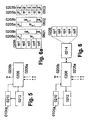
- FIG. 1 shows a reconfigurable data processing unit (VPU) ( 0101 ).
- a configuration unit (CT, 0103 ) for the control and execution of the configuration and reconfiguration is superordinated to an array of PAEs ( 0102 ) which are configurable and reconfigurable independently from one another.
- PAEs 0102
- a central clock generator 0104
- the clock rate of the central clock generator may be preselected by configuration unit 0103 .
- the clock rate of each PAE and/or groups of PAEs and their bus connections may also be preselected by configuration unit 0103 .
- configuration unit 0103 feeds configuring data via a configuration line 0103 a into respective cells 0102 of which only one is illustrated as an example. Furthermore, the clock signal of central clock generator 0104 is fed to cell 0102 via a clock line 0104 a .
- reconfigurable cell 0102 communicates with other cells and additionally has a data processing unit, e.g., an arithmetic logic unit ALU 0206 , and preferably an internal data memory 0207 and a configuration memory 0208 into which configuring instructions from configuration unit 0103 are fed via a configuration instruction extractor 0209 in order to configure the data processing unit, e.g., ALU 0206 , as a response.
- a data processing unit e.g., an arithmetic logic unit ALU 0206
- ALU 0206 arithmetic logic unit
- configuration memory 0208 into which configuring instructions from configuration unit 0103 are fed via a configuration instruction extractor 0209 in order to configure the data processing unit, e.g., ALU 0206 , as a response.
- configuration (instruction) extractor 0209 is connected to a frequency divider/multiplier factor preselecting input 0210 a of a frequency divider/frequency multiplier 0210 which is designed to divide or multiply the clock signal of central clock generator 0104 on clock line 0104 a according to a clock ratio preselected via input 0210 a and to feed the clock signal to the data processing unit, e.g., arithmetic logic unit ALU 0206 , and possibly other units of reconfigurable cell 0102 via a line 0211 .
- the data processing unit e.g., arithmetic logic unit ALU 0206 , and possibly other units of reconfigurable cell 0102 via a line 0211 .
- 0210 may be activated in such a way that the frequency is controlled depending on the data reception or the data transmission.
- a multiplexer 0213 for selecting different configurations and/or configuration groups may optionally be integrated dependent on 0212 .
- the multiplexer may optionally be activated by a sequencer 0214 in order to make sequential data processing possible.
- intermediate results may be managed in data memory 0207 .
- configuration unit 0103 is designed in such a way that, together with a configuring signal with which a configuration word is fed via configuration line 0103 a via configuration word extractor 0209 to data processing unit 0206 or upstream and/or downstream and/or associated memory 0208 , a clock dividing/multiplying signal may also be transmitted which is extracted by configuration word extractor 0209 and transmitted to frequency divider/multiplier 0210 , so that, as a response, 0210 may clock data processing unit 0206 and possibly also other units.
- unit 0209 to vary clocking of an individual data processing unit 0206 with reference to a central clock unit 0104 , via data bus monitoring circuit 0212 , for example.
- an entire field of all reconfigurable logic units 0102 may be operated using the above-described embodiment, but possibly also by implementing the units in a different way.
- a 3 ⁇ 3 field of reconfigurable cells is configured in such a way, according to FIG. 3 a , that a first cell 0102 a is used for analyzing an input/output signal.
- Cells 0102 b , 0102 c are presently not needed and are therefore denoted as not configured (n. c.).
- Cells 0102 d through 0102 i together form a group which executes a complex arithmetic operation; an addition takes place in cell 0102 d , a subtraction takes place in cell 0102 e , a multiplication takes place in cell 0102 f , a loop is run in cell 0102 g , a multiple addition being executed within the loop, a division takes place in cell 0102 h , and an addition in turn takes place in cell 0102 i .
- Cells 0102 d through 0102 i are connected to one another in group 0301 , indicated by dot and dash lines, in such a way that data is sequentially and pipeline-like processed by the cells. As is indicated in the second row of the table in FIG.
- the operations within cells 0102 d and 0102 e are executed in a different number of clock cycles.
- the number of clock cycles is denoted there and it is clear that an addition or a subtraction may be executed in one clock cycle; the division, however, requires 32 clock cycles.
- the third line of the table in FIG. 3 b denotes which value is assigned to the frequency divider of each cell in order to achieve optimum power usage at a constant data throughput through the cell. Only the cell in which the division takes place is operated at the highest clock; the clock ratio here is 1. This cell requires the longest time for the operation assigned to it.
- the processor unit having the separately clockable reconfigurable logic cells is operated in an application where the voltage may drop, e.g., due to exhausting voltage supply capacities, it may be provided that, at a drop in the supply voltage, the entire frequency is reduced to a critical value U1; all cells are subsequently clocked slower by one half so that division cell 0102 h too runs only at 128 MHz, while cell 0102 d is clocked at 4 MHz.
- Cell 0102 a executing a query of the mouse pointer having a lower priority, is no longer clocked at 8 MHz as previously but rather at 2 MHz, i.e., depending on the prioritization, different slowdowns according to the importance of the task are assigned to the respective groups at a voltage drop or under other circumstances.
- the heat generation in the logic cell field may be further reduced by an additional clock rate reduction for the logic cells, as is indicated in the last row of FIG. 3 b .
- a particular individual sensor for determining the condition such as the supply voltage and/or the temperature may be provided whose sensor signal is fed to the cells in a conditioned manner; a corresponding sensor system may be assigned to each cell and/or the central clock is possibly modifiable.
- a hardware switch or a software switch may be provided with which the user indicates that only low clocking or higher clocking is desired. This makes an even more economical and targeted handling of the available power possible. It may be provided in particular that, at the user's request or at an external request, the central clock rate in total may be reduced; the clock divider ratios within the cell array, however, are not changed in order to avoid the requirement of reconfiguring all cells, e.g., at an extreme temperature rise. Moreover, it should be pointed out that a hysteresis characteristic may be provided in determining the clock rates, when a temperature-sensitive change of the clock frequencies is to be performed, for example.
- FIG. 4 shows the data processing unit (VPU) according to FIG. 1 .
- VPU data processing unit
- Different groups within the VPU are operated using different frequencies f which are derived from a frequency normal n generated by 0104 .
- frequencies f which are derived from a frequency normal n generated by 0104 .
- multiple frequency normals n 1 . . . n n
- FIG. 5 shows a simple exemplary embodiment for the operation of a PAE according to FIG. 2 .
- a data bus ( 0205 a ) delivers operands ia1 and ia2 to an ALU ( 0206 ) which in turn delivers the result of the computation oa to 0205 b .
- the PAE is only activated, i.e., clocked and/or supplied with current, when data bus monitoring circuit 0212 recognizes the acceptance of the previous result oa by the receiver and the arrival of operands ia1 and ia2 necessary for the operation. In other words, the PAE is only activated when all working conditions and requirements are met.
- the clock release is carried out by 0210 , the clock source is 0104 a.
- FIG. 6 corresponds to FIG. 5 with the exception that a sequencer ( 0214 ) is additionally activated which controls a multicyclical configuration (e.g., a complex computation such as a matrix multiplication or the like).
- the sequencer extracts the operations from the configuration memory or from a section of the configuration memory.
- operations op1, op2, op3, op4, op5 are carried out sequentially.
- Result oa is conveyed after completion and the PAE has to be activated again.
- the data transmission occurring on data bus 0205 a/b is illustrated in FIG. 6 a . It should be pointed out that the data routing via the bus may take place in a conventional manner, i.e., collision and deadlock situations may be prevented for one configuration at a time in a conventional manner.
- operands is mist be available via 0205 a ( 0601 ); the data transmissions for the remaining cycles may be undefined in principle.
- 0205 a may preferably transmit the subsequent operands ( 0602 ) for which the execution time of op2, op3, op4, op5 is available, thus creating a temporal decoupling, allowing the use of slower and/or, in particular, longer bus systems.
- data of other configurations may alternatively ( 0603 ) be transmitted via the same bus system 0205 a using a time-division multiplex method.
- result oa is applied to bus 0205 b ( 0601 ); the data transmissions for the remaining cycles may be undefined in principle.
- the time prior to op5, i.e., during the execution of op1, op2, op3, op4, may be used for transmitting the previous result ( 0602 ). This again creates a temporal decoupling, allowing the use of slower and/or, in particular, longer bus systems.
- data of other configurations may alternatively ( 0603 ) be transmitted via the same bus system 0205 b using a time-division multiplex method.
- 0210 may use a PLL.
- a PLL may be used in particular in such a way that the operating clock of the PAE for executing op1, op2, op3, op4, op5 is five times that of the bus clock.
- the PAE may act as a PAE without a sequencer having only one (unicyclical) configuration and the same clock as the bus clock.
- FIG. 7 corresponds to FIG. 6 plus the addition that multiple configuration groups (ga, gb, gc) share the PAE in a time-division multiplexed manner and each group has connections to a separate (space-division multiplexed) bus system (ia/oa, ib/ob, ic/oc).
- a multiplexer in 0214 cyclically selects the groups ga, gb, gc.
- the data monitoring circuit 0212 generates a valid execution release (condition) for a configuration group, the particular configuration group is executed; otherwise the execution release (condition) may be awaited or, preferably, a different subsequent configuration group may be selected.
- the configuration groups may be run through cyclically.
- the configuration words may be executed sequentially in 0214 using a sequencer.
- FIG. 7 a shows the bus transmissions according to the example in FIG. 7 .
- 0701 corresponds to 0601
- 0702 corresponds to 0602
- 0703 corresponds to 0603 ; a separate bus system is used thereby for each group ga, gb, gc.
- a possible bus transmission using a time-division multiplex for the bus systems is illustrated in 0704 .
- the input data of all groups is transmitted via an input bus system and the output data of all groups is transmitted via an output bus system.
- the undefined intermediate cycles are either unused or are free for other data transmissions.
Abstract
Description
-
- Sequencer 1 (Seq1) requires 10 operations for processing a data packet,
- Sequencer 2 (Seq2) requires 5 operations for processing a data packet,
- Sequencer 3 (Seq3) requires 20 operations for processing a data packet.
Fmax=F Seq2/4=F Seq1/2=F Seq3
or at a maximum operating frequency of, for example, 100 MHz: FSeq1=50 MHz, FSeq2=25 MHz,
-
- 1) Clock dividers, individually programmable per PAE, which enable an individually configurable divider ratio based on one or more mutual base clocks.
- 2) Clock multipliers (PLLs), individually programmable per PAE, which enable an individually configurable divider ratio based on one or more mutual base clocks.
- 3) Deriving the particular PAE clock from the data stream of the particular data to be processed, e.g., by oversampling.
-
- a) An input buffer is largely full and/or the filling level rises abruptly: Clocking increase to accelerate processing.
- b) An input buffer is largely empty and/or the filling level drops abruptly: Clocking decrease to decelerate processing.
- c) An output buffer is largely full and/or the filling level rises abruptly: Clocking decrease to decelerate processing.
- d) An output buffer is largely empty and/or the filling level drops abruptly: Clocking increase to accelerate processing.
Claims (45)
Priority Applications (2)
| Application Number | Priority Date | Filing Date | Title |
|---|---|---|---|
| US14/219,945 US9552047B2 (en) | 2001-03-05 | 2014-03-19 | Multiprocessor having runtime adjustable clock and clock dependent power supply |
| US15/408,358 US10331194B2 (en) | 2001-03-05 | 2017-01-17 | Methods and devices for treating and processing data |
Applications Claiming Priority (107)
| Application Number | Priority Date | Filing Date | Title |
|---|---|---|---|
| DE10110530 | 2001-03-05 | ||
| DE10110530 | 2001-03-05 | ||
| DE10110530.4 | 2001-03-05 | ||
| DE10111014 | 2001-03-07 | ||
| DE10111014.6 | 2001-03-07 | ||
| DE10111014 | 2001-03-07 | ||
| EPPCT/EP01/06703 | 2001-06-13 | ||
| PCT/EP2001/006703 WO2002013000A2 (en) | 2000-06-13 | 2001-06-13 | Pipeline configuration unit protocols and communication |
| WOPCT/EP01/06703 | 2001-06-13 | ||
| DE10129237.6 | 2001-06-20 | ||
| EP1115021.6 | 2001-06-20 | ||
| EP1115021 | 2001-06-20 | ||
| EP01115021 | 2001-06-20 | ||
| DE10129237 | 2001-06-20 | ||
| DE10135210.7 | 2001-06-24 | ||
| DE10135210 | 2001-07-24 | ||
| WOPCT/EP01/08534 | 2001-07-24 | ||
| DE10135211.5 | 2001-07-24 | ||
| DE10135210 | 2001-07-24 | ||
| EPPCT/EP01/08534 | 2001-07-24 | ||
| DE10135211 | 2001-07-24 | ||
| DE10135211 | 2001-07-24 | ||
| PCT/EP2001/008534 WO2002008964A2 (en) | 2000-07-24 | 2001-07-24 | Integrated circuit |
| DE10139170.6 | 2001-08-16 | ||
| DE10139170 | 2001-08-16 | ||
| DE10139170 | 2001-08-16 | ||
| DE10142231 | 2001-08-29 | ||
| DE10142231 | 2001-08-29 | ||
| DE10142231.8 | 2001-08-29 | ||
| DE10142894 | 2001-09-03 | ||
| DE10142903 | 2001-09-03 | ||
| DE10142894 | 2001-09-03 | ||
| DE10142903 | 2001-09-03 | ||
| DE10142904 | 2001-09-03 | ||
| DE10142903.7 | 2001-09-03 | ||
| DE10142904 | 2001-09-03 | ||
| DE10142904.5 | 2001-09-03 | ||
| DE10142894.4 | 2001-09-03 | ||
| DE10144733 | 2001-09-11 | ||
| DE10144733 | 2001-09-11 | ||
| DE10144732 | 2001-09-11 | ||
| DE10144732 | 2001-09-11 | ||
| DE10144732.9 | 2001-09-11 | ||
| DE10144733.7 | 2001-09-11 | ||
| DE10145792.8 | 2001-09-17 | ||
| DE10145792 | 2001-09-17 | ||
| DE10145795 | 2001-09-17 | ||
| DE10145795.2 | 2001-09-17 | ||
| DE10145792 | 2001-09-17 | ||
| DE10145795 | 2001-09-17 | ||
| DE10146132 | 2001-09-19 | ||
| DE10146132 | 2001-09-19 | ||
| DE10146132.1 | 2001-09-19 | ||
| EPPCT/EP01/11299 | 2001-09-30 | ||
| WOPCT/EP01/11299 | 2001-09-30 | ||
| EP0111299 | 2001-09-30 | ||
| PCT/EP2001/011593 WO2002029600A2 (en) | 2000-10-06 | 2001-10-08 | Cell system with segmented intermediate cell structure |
| EPPCT/EP01/11593 | 2001-10-08 | ||
| WOPCT/EP01/11593 | 2001-10-08 | ||
| DE10154259.3 | 2001-11-05 | ||
| DE10154260.7 | 2001-11-05 | ||
| DE10154259 | 2001-11-05 | ||
| DE10154259 | 2001-11-05 | ||
| DE10154260 | 2001-11-05 | ||
| DE10154260 | 2001-11-05 | ||
| EP11299237 | 2001-12-14 | ||
| EP1129923.7 | 2001-12-14 | ||
| EP1129923 | 2001-12-14 | ||
| EP2001331 | 2002-01-18 | ||
| EP2001331.4 | 2002-01-18 | ||
| DE10202044 | 2002-01-19 | ||
| DE10202044 | 2002-01-19 | ||
| DE10202044.2 | 2002-01-19 | ||
| DE10202175.9 | 2002-01-20 | ||
| DE10202175 | 2002-01-20 | ||
| DE10202175 | 2002-01-20 | ||
| DE10206653.1 | 2002-02-15 | ||
| DE10206653 | 2002-02-15 | ||
| DE10206653 | 2002-02-15 | ||
| DE10206857 | 2002-02-18 | ||
| DE10206856 | 2002-02-18 | ||
| DE10206857 | 2002-02-18 | ||
| DE10206857.7 | 2002-02-18 | ||
| DE10206856.9 | 2002-02-18 | ||
| DE10206856 | 2002-02-18 | ||
| DE10207226 | 2002-02-21 | ||
| DE10207226.4 | 2002-02-21 | ||
| DE10207224 | 2002-02-21 | ||
| DE10207225 | 2002-02-21 | ||
| DE10207226 | 2002-02-21 | ||
| DE10207225.6 | 2002-02-21 | ||
| DE10207224.8 | 2002-02-21 | ||
| DE10207224 | 2002-02-21 | ||
| DE10207225 | 2002-02-21 | ||
| DE10208434 | 2002-02-27 | ||
| DE10208435.1 | 2002-02-27 | ||
| DE10208434 | 2002-02-27 | ||
| DE10208434.3 | 2002-02-27 | ||
| DE10208435 | 2002-02-27 | ||
| DE10208435 | 2002-02-27 | ||
| US10/469,909 US7444531B2 (en) | 2001-03-05 | 2002-03-05 | Methods and devices for treating and processing data |
| PCT/EP2002/002402 WO2002071196A2 (en) | 2001-03-05 | 2002-03-05 | Methods and devices for treating and processing data |
| DE10129237A DE10129237A1 (en) | 2000-10-09 | 2002-06-20 | Integrated cell matrix circuit has at least 2 different types of cells with interconnection terminals positioned to allow mixing of different cell types within matrix circuit |
| US12/257,075 US8099618B2 (en) | 2001-03-05 | 2008-10-23 | Methods and devices for treating and processing data |
| US12/570,984 US8312301B2 (en) | 2001-03-05 | 2009-09-30 | Methods and devices for treating and processing data |
| US13/653,639 US9075605B2 (en) | 2001-03-05 | 2012-10-17 | Methods and devices for treating and processing data |
| US14/219,945 US9552047B2 (en) | 2001-03-05 | 2014-03-19 | Multiprocessor having runtime adjustable clock and clock dependent power supply |
Related Parent Applications (1)
| Application Number | Title | Priority Date | Filing Date |
|---|---|---|---|
| US13/653,639 Division US9075605B2 (en) | 2001-03-05 | 2012-10-17 | Methods and devices for treating and processing data |
Related Child Applications (1)
| Application Number | Title | Priority Date | Filing Date |
|---|---|---|---|
| US15/408,358 Continuation US10331194B2 (en) | 2001-03-05 | 2017-01-17 | Methods and devices for treating and processing data |
Publications (2)
| Publication Number | Publication Date |
|---|---|
| US20140208143A1 US20140208143A1 (en) | 2014-07-24 |
| US9552047B2 true US9552047B2 (en) | 2017-01-24 |
Family
ID=51211419
Family Applications (1)
| Application Number | Title | Priority Date | Filing Date |
|---|---|---|---|
| US14/219,945 Expired - Lifetime US9552047B2 (en) | 2001-03-05 | 2014-03-19 | Multiprocessor having runtime adjustable clock and clock dependent power supply |
Country Status (1)
| Country | Link |
|---|---|
| US (1) | US9552047B2 (en) |
Cited By (6)
| Publication number | Priority date | Publication date | Assignee | Title |
|---|---|---|---|---|
| US9691019B1 (en) * | 2017-03-07 | 2017-06-27 | Google Inc. | Depth concatenation using a matrix computation unit |
| US20170192481A1 (en) * | 2001-03-05 | 2017-07-06 | Pact Xpp Technologies Ag | Methods and devices for treating and processing data |
| US20180121130A1 (en) * | 2016-10-27 | 2018-05-03 | Samsung Electronics Co., Ltd. | Software stack and programming for dpu operations |
| US10528513B1 (en) | 2018-04-30 | 2020-01-07 | Xilinx, Inc. | Circuit for and method of providing a programmable connector of an integrated circuit device |
| US10699182B2 (en) | 2017-03-07 | 2020-06-30 | Google Llc | Depth concatenation using a matrix computation unit |
| US10885996B2 (en) | 1997-10-08 | 2021-01-05 | Pact Xpp Schweiz Ag | Processor having a programmable function unit |
Families Citing this family (2)
| Publication number | Priority date | Publication date | Assignee | Title |
|---|---|---|---|---|
| KR101840852B1 (en) | 2011-10-10 | 2018-03-22 | 삼성전자주식회사 | Surface temperature management method of mobile device and memory thermal management method of multichip package |
| JP2022042856A (en) * | 2020-09-03 | 2022-03-15 | 富士フイルムビジネスイノベーション株式会社 | Information processing device, and program |
Citations (240)
| Publication number | Priority date | Publication date | Assignee | Title |
|---|---|---|---|---|
| US3473160A (en) | 1966-10-10 | 1969-10-14 | Stanford Research Inst | Electronically controlled microelectronic cellular logic array |
| US3531662A (en) | 1967-04-10 | 1970-09-29 | Sperry Rand Corp | Batch fabrication arrangement for integrated circuits |
| US4020469A (en) | 1975-04-09 | 1977-04-26 | Frank Manning | Programmable arrays |
| US4412303A (en) | 1979-11-26 | 1983-10-25 | Burroughs Corporation | Array processor architecture |
| US4454578A (en) | 1980-05-19 | 1984-06-12 | Hitachi, Ltd. | Data processing unit with pipelined operands |
| US4539637A (en) | 1982-08-26 | 1985-09-03 | At&T Bell Laboratories | Method and apparatus for handling interprocessor calls in a multiprocessor system |
| US4577293A (en) | 1984-06-01 | 1986-03-18 | International Business Machines Corporation | Distributed, on-chip cache |
| US4642487A (en) | 1984-09-26 | 1987-02-10 | Xilinx, Inc. | Special interconnect for configurable logic array |
| US4700187A (en) | 1985-12-02 | 1987-10-13 | Concurrent Logic, Inc. | Programmable, asynchronous logic cell and array |
| US4706216A (en) | 1985-02-27 | 1987-11-10 | Xilinx, Inc. | Configurable logic element |
| US4722084A (en) | 1985-10-02 | 1988-01-26 | Itt Corporation | Array reconfiguration apparatus and methods particularly adapted for use with very large scale integrated circuits |
| US4724307A (en) | 1986-04-29 | 1988-02-09 | Gtech Corporation | Marked card reader |
| US4748580A (en) | 1985-08-30 | 1988-05-31 | Advanced Micro Devices, Inc. | Multi-precision fixed/floating-point processor |
| US4768196A (en) | 1986-10-28 | 1988-08-30 | Silc Technologies, Inc. | Programmable logic array |
| US4786904A (en) | 1986-12-15 | 1988-11-22 | Zoran Corporation | Electronically programmable gate array having programmable interconnect lines |
| US4791603A (en) | 1986-07-18 | 1988-12-13 | Honeywell Inc. | Dynamically reconfigurable array logic |
| US4837735A (en) | 1987-06-09 | 1989-06-06 | Martin Marietta Energy Systems, Inc. | Parallel machine architecture for production rule systems |
| US4862407A (en) | 1987-10-05 | 1989-08-29 | Motorola, Inc. | Digital signal processing apparatus |
| US4918440A (en) | 1986-11-07 | 1990-04-17 | Furtek Frederick C | Programmable logic cell and array |
| US4959781A (en) | 1988-05-16 | 1990-09-25 | Stardent Computer, Inc. | System for assigning interrupts to least busy processor that already loaded same class of interrupt routines |
| US4967340A (en) | 1985-06-12 | 1990-10-30 | E-Systems, Inc. | Adaptive processing system having an array of individually configurable processing components |
| US5036473A (en) | 1988-10-05 | 1991-07-30 | Mentor Graphics Corporation | Method of using electronically reconfigurable logic circuits |
| US5055997A (en) | 1988-01-13 | 1991-10-08 | U.S. Philips Corporation | System with plurality of processing elememts each generates respective instruction based upon portions of individual word received from a crossbar switch |
| US5070475A (en) | 1985-11-14 | 1991-12-03 | Data General Corporation | Floating point unit interface |
| US5081575A (en) | 1987-11-06 | 1992-01-14 | Oryx Corporation | Highly parallel computer architecture employing crossbar switch with selectable pipeline delay |
| US5103311A (en) | 1988-01-11 | 1992-04-07 | U.S. Philips Corporation | Data processing module and video processing system incorporating same |
| US5113498A (en) | 1987-11-10 | 1992-05-12 | Echelon Corporation | Input/output section for an intelligent cell which provides sensing, bidirectional communications and control |
| US5119499A (en) | 1988-05-27 | 1992-06-02 | Hitachi Ltd. | Host processor which includes apparatus for performing coprocessor functions |
| US5123109A (en) | 1983-05-31 | 1992-06-16 | Thinking Machines Corporation | Parallel processor including a processor array with plural data transfer arrangements including (1) a global router and (2) a proximate-neighbor transfer system |
| US5144166A (en) | 1990-11-02 | 1992-09-01 | Concurrent Logic, Inc. | Programmable logic cell and array |
| US5197016A (en) | 1988-01-13 | 1993-03-23 | International Chip Corporation | Integrated silicon-software compiler |
| US5212777A (en) | 1989-11-17 | 1993-05-18 | Texas Instruments Incorporated | Multi-processor reconfigurable in single instruction multiple data (SIMD) and multiple instruction multiple data (MIMD) modes and method of operation |
| US5243238A (en) | 1989-03-17 | 1993-09-07 | Algotronix Limited | Configurable cellular array |
| US5245227A (en) | 1990-11-02 | 1993-09-14 | Atmel Corporation | Versatile programmable logic cell for use in configurable logic arrays |
| US5261113A (en) | 1988-01-25 | 1993-11-09 | Digital Equipment Corporation | Apparatus and method for single operand register array for vector and scalar data processing operations |
| USRE34444E (en) | 1988-01-13 | 1993-11-16 | Xilinx, Inc. | Programmable logic device |
| US5287511A (en) | 1988-07-11 | 1994-02-15 | Star Semiconductor Corporation | Architectures and methods for dividing processing tasks into tasks for a programmable real time signal processor and tasks for a decision making microprocessor interfacing therewith |
| US5296759A (en) | 1991-08-29 | 1994-03-22 | National Semiconductor Corporation | Diagonal wiring between abutting logic cells in a configurable logic array |
| US5298805A (en) | 1991-08-29 | 1994-03-29 | National Semiconductor Corporation | Versatile and efficient cell-to-local bus interface in a configurable logic array |
| US5301340A (en) | 1990-10-31 | 1994-04-05 | International Business Machines Corporation | IC chips including ALUs and identical register files whereby a number of ALUs directly and concurrently write results to every register file per cycle |
| US5327570A (en) | 1991-07-22 | 1994-07-05 | International Business Machines Corporation | Multiprocessor system having local write cache within each data processor node |
| US5355508A (en) | 1990-05-07 | 1994-10-11 | Mitsubishi Denki Kabushiki Kaisha | Parallel data processing system combining a SIMD unit with a MIMD unit and sharing a common bus, memory, and system controller |
| US5357152A (en) | 1992-11-10 | 1994-10-18 | Infinite Technology Corporation | Logic system of logic networks with programmable selected functions and programmable operational controls |
| US5361373A (en) | 1992-12-11 | 1994-11-01 | Gilson Kent L | Integrated circuit computing device comprising a dynamically configurable gate array having a microprocessor and reconfigurable instruction execution means and method therefor |
| DE4416881A1 (en) | 1993-05-13 | 1994-11-17 | Martin Vorbach | Data processing device |
| US5386518A (en) | 1993-02-12 | 1995-01-31 | Hughes Aircraft Company | Reconfigurable computer interface and method |
| US5386154A (en) | 1992-07-23 | 1995-01-31 | Xilinx, Inc. | Compact logic cell for field programmable gate array chip |
| US5394030A (en) | 1992-11-10 | 1995-02-28 | Infinite Technology Corporation | Programmable logic device |
| US5408129A (en) | 1990-04-18 | 1995-04-18 | Rambus, Inc. | Integrated circuit I/O using a high performance bus interface |
| US5410723A (en) | 1989-11-21 | 1995-04-25 | Deutsche Itt Industries Gmbh | Wavefront array processor for blocking the issuance of first handshake signal (req) by the presence of second handshake signal (ack) which indicates the readyness of the receiving cell |
| US5412795A (en) | 1992-02-25 | 1995-05-02 | Micral, Inc. | State machine having a variable timing mechanism for varying the duration of logical output states of the state machine based on variation in the clock frequency |
| US5421019A (en) | 1988-10-07 | 1995-05-30 | Martin Marietta Corporation | Parallel data processor |
| US5426378A (en) | 1994-04-20 | 1995-06-20 | Xilinx, Inc. | Programmable logic device which stores more than one configuration and means for switching configurations |
| US5430885A (en) | 1986-10-30 | 1995-07-04 | Hitachi, Ltd. | Multi-processor system and co-processor used for the same |
| US5440711A (en) | 1990-03-05 | 1995-08-08 | Mitsubishi Denki Kabushiki Kaisha | Method for controlling DRAM memory in a microcomputer |
| US5448496A (en) | 1988-10-05 | 1995-09-05 | Quickturn Design Systems, Inc. | Partial crossbar interconnect architecture for reconfigurably connecting multiple reprogrammable logic devices in a logic emulation system |
| WO1995025306A2 (en) | 1994-03-14 | 1995-09-21 | Stanford University | Distributed shared-cache for multi-processors |
| US5459846A (en) | 1988-12-02 | 1995-10-17 | Hyatt; Gilbert P. | Computer architecture system having an imporved memory |
| WO1995028671A1 (en) | 1994-04-18 | 1995-10-26 | Green Logic Inc. | An improved system logic controller for digital computers |
| US5469003A (en) | 1992-11-05 | 1995-11-21 | Xilinx, Inc. | Hierarchically connectable configurable cellular array |
| US5488582A (en) | 1992-07-02 | 1996-01-30 | Atmel Corporation | Non-disruptive, randomly addressable memory system |
| US5502838A (en) * | 1994-04-28 | 1996-03-26 | Consilium Overseas Limited | Temperature management for integrated circuits |
| US5504439A (en) | 1994-04-01 | 1996-04-02 | Xilinx, Inc. | I/O interface cell for use with optional pad |
| US5525971A (en) | 1993-09-23 | 1996-06-11 | Advanced Risc Machines Limited | Integrated circuit |
| US5572680A (en) | 1992-12-18 | 1996-11-05 | Fujitsu Limited | Method and apparatus for processing and transferring data to processor and/or respective virtual processor corresponding to destination logical processor number |
| US5574930A (en) | 1994-08-12 | 1996-11-12 | University Of Hawaii | Computer system and method using functional memory |
| US5581778A (en) | 1992-08-05 | 1996-12-03 | David Sarnoff Researach Center | Advanced massively parallel computer using a field of the instruction to selectively enable the profiling counter to increase its value in response to the system clock |
| US5596743A (en) | 1993-05-28 | 1997-01-21 | Regents Of The University Of California | Field programmable logic device with dynamic interconnections to a dynamic logic core |
| US5600597A (en) | 1995-05-02 | 1997-02-04 | Xilinx, Inc. | Register protection structure for FPGA |
| US5608342A (en) | 1995-10-23 | 1997-03-04 | Xilinx, Inc. | Hierarchical programming of electrically configurable integrated circuits |
| US5619720A (en) | 1994-10-04 | 1997-04-08 | Analog Devices, Inc. | Digital signal processor having link ports for point-to-point communication |
| US5625836A (en) | 1990-11-13 | 1997-04-29 | International Business Machines Corporation | SIMD/MIMD processing memory element (PME) |
| US5631578A (en) | 1995-06-02 | 1997-05-20 | International Business Machines Corporation | Programmable array interconnect network |
| US5635851A (en) | 1996-02-02 | 1997-06-03 | Xilinx, Inc. | Read and writable data bus particularly for programmable logic devices |
| US5642058A (en) | 1995-10-16 | 1997-06-24 | Xilinx , Inc. | Periphery input/output interconnect structure |
| US5646546A (en) | 1995-06-02 | 1997-07-08 | International Business Machines Corporation | Programmable logic cell having configurable gates and multiplexers |
| US5646544A (en) | 1995-06-05 | 1997-07-08 | International Business Machines Corporation | System and method for dynamically reconfiguring a programmable gate array |
| US5651137A (en) | 1995-04-12 | 1997-07-22 | Intel Corporation | Scalable cache attributes for an input/output bus |
| US5652529A (en) | 1995-06-02 | 1997-07-29 | International Business Machines Corporation | Programmable array clock/reset resource |
| US5656950A (en) | 1995-10-26 | 1997-08-12 | Xilinx, Inc. | Interconnect lines including tri-directional buffer circuits |
| US5659785A (en) | 1995-02-10 | 1997-08-19 | International Business Machines Corporation | Array processor communication architecture with broadcast processor instructions |
| US5671432A (en) | 1995-06-02 | 1997-09-23 | International Business Machines Corporation | Programmable array I/O-routing resource |
| US5675777A (en) | 1990-01-29 | 1997-10-07 | Hipercore, Inc. | Architecture for minimal instruction set computing system |
| US5675262A (en) | 1995-10-26 | 1997-10-07 | Xilinx, Inc. | Fast carry-out scheme in a field programmable gate array |
| US5682491A (en) | 1994-12-29 | 1997-10-28 | International Business Machines Corporation | Selective processing and routing of results among processors controlled by decoding instructions using mask value derived from instruction tag and processor identifier |
| US5685004A (en) | 1990-03-06 | 1997-11-04 | Xerox Corporation | Multi-segmented bus and method of operation |
| US5687325A (en) | 1996-04-19 | 1997-11-11 | Chang; Web | Application specific field programmable gate array |
| US5696976A (en) | 1990-12-21 | 1997-12-09 | Intel Corporation | Protocol for interrupt bus arbitration in a multi-processor system |
| US5701091A (en) | 1995-05-02 | 1997-12-23 | Xilinx, Inc. | Routing resources for hierarchical FPGA |
| US5705938A (en) | 1995-05-02 | 1998-01-06 | Xilinx, Inc. | Programmable switch for FPGA input/output signals |
| US5715476A (en) | 1995-12-29 | 1998-02-03 | Intel Corporation | Method and apparatus for controlling linear and toggle mode burst access sequences using toggle mode increment logic |
| US5721921A (en) | 1995-05-25 | 1998-02-24 | Cray Research, Inc. | Barrier and eureka synchronization architecture for multiprocessors |
| US5734869A (en) | 1995-09-06 | 1998-03-31 | Chen; Duan-Ping | High speed logic circuit simulator |
| US5742180A (en) | 1995-02-10 | 1998-04-21 | Massachusetts Institute Of Technology | Dynamically programmable gate array with multiple contexts |
| US5748979A (en) | 1995-04-05 | 1998-05-05 | Xilinx Inc | Reprogrammable instruction set accelerator using a plurality of programmable execution units and an instruction page table |
| US5752035A (en) | 1995-04-05 | 1998-05-12 | Xilinx, Inc. | Method for compiling and executing programs for reprogrammable instruction set accelerator |
| US5761484A (en) | 1994-04-01 | 1998-06-02 | Massachusetts Institute Of Technology | Virtual interconnections for reconfigurable logic systems |
| US5765009A (en) | 1994-02-22 | 1998-06-09 | Fujitsu Limited | Barrier synchronization system in parallel data processing |
| US5774704A (en) | 1996-07-29 | 1998-06-30 | Silicon Graphics, Inc. | Apparatus and method for dynamic central processing unit clock adjustment |
| US5778439A (en) | 1995-08-18 | 1998-07-07 | Xilinx, Inc. | Programmable logic device with hierarchical confiquration and state storage |
| US5781756A (en) | 1994-04-01 | 1998-07-14 | Xilinx, Inc. | Programmable logic device with partially configurable memory cells and a method for configuration |
| US5784636A (en) | 1996-05-28 | 1998-07-21 | National Semiconductor Corporation | Reconfigurable computer architecture for use in signal processing applications |
| US5805477A (en) | 1996-09-26 | 1998-09-08 | Hewlett-Packard Company | Arithmetic cell for field programmable devices |
| US5808487A (en) | 1994-11-30 | 1998-09-15 | Hitachi Micro Systems, Inc. | Multi-directional small signal transceiver/repeater |
| US5812844A (en) | 1995-12-07 | 1998-09-22 | Microsoft Corporation | Method and system for scheduling the execution of threads using optional time-specific scheduling constraints |
| US5815004A (en) | 1995-10-16 | 1998-09-29 | Xilinx, Inc. | Multi-buffered configurable logic block output lines in a field programmable gate array |
| US5828858A (en) | 1996-09-16 | 1998-10-27 | Virginia Tech Intellectual Properties, Inc. | Worm-hole run-time reconfigurable processor field programmable gate array (FPGA) |
| US5832288A (en) | 1996-10-18 | 1998-11-03 | Samsung Electronics Co., Ltd. | Element-select mechanism for a vector processor |
| US5857109A (en) | 1992-11-05 | 1999-01-05 | Giga Operations Corporation | Programmable logic device for real time video processing |
| US5893165A (en) | 1996-07-01 | 1999-04-06 | Sun Microsystems, Inc. | System and method for parallel execution of memory transactions using multiple memory models, including SSO, TSO, PSO and RMO |
| US5892962A (en) | 1996-11-12 | 1999-04-06 | Lucent Technologies Inc. | FPGA-based processor |
| US5894565A (en) | 1996-05-20 | 1999-04-13 | Atmel Corporation | Field programmable gate array with distributed RAM and increased cell utilization |
| US5898602A (en) | 1996-01-25 | 1999-04-27 | Xilinx, Inc. | Carry chain circuit with flexible carry function for implementing arithmetic and logical functions |
| US5905875A (en) | 1995-04-28 | 1999-05-18 | Fujitsu Limited | Multiprocessor system connected by a duplicated system bus having a bus status notification line |
| US5915123A (en) | 1997-10-31 | 1999-06-22 | Silicon Spice | Method and apparatus for controlling configuration memory contexts of processing elements in a network of multiple context processing elements |
| US5913925A (en) | 1996-12-16 | 1999-06-22 | International Business Machines Corporation | Method and system for constructing a program including out-of-order threads and processor and method for executing threads out-of-order |
| US5933642A (en) | 1995-04-17 | 1999-08-03 | Ricoh Corporation | Compiling system and method for reconfigurable computing |
| US5943242A (en) | 1995-11-17 | 1999-08-24 | Pact Gmbh | Dynamically reconfigurable data processing system |
| US5956518A (en) | 1996-04-11 | 1999-09-21 | Massachusetts Institute Of Technology | Intermediate-grain reconfigurable processing device |
| US5966534A (en) | 1997-06-27 | 1999-10-12 | Cooke; Laurence H. | Method for compiling high level programming languages into an integrated processor with reconfigurable logic |
| US5978830A (en) | 1997-02-24 | 1999-11-02 | Hitachi, Ltd. | Multiple parallel-job scheduling method and apparatus |
| US5978583A (en) | 1995-08-07 | 1999-11-02 | International Business Machines Corp. | Method for resource control in parallel environments using program organization and run-time support |
| US5990910A (en) | 1998-03-24 | 1999-11-23 | Ati Technologies, Inc. | Method and apparatus for co-processing multi-formatted data |
| US5991900A (en) | 1998-06-15 | 1999-11-23 | Sun Microsystems, Inc. | Bus controller |
| US6011407A (en) | 1997-06-13 | 2000-01-04 | Xilinx, Inc. | Field programmable gate array with dedicated computer bus interface and method for configuring both |
| US6023564A (en) | 1996-07-19 | 2000-02-08 | Xilinx, Inc. | Data processing system using a flash reconfigurable logic device as a dynamic execution unit for a sequence of instructions |
| US6023742A (en) | 1996-07-18 | 2000-02-08 | University Of Washington | Reconfigurable computing architecture for providing pipelined data paths |
| US6034542A (en) | 1997-10-14 | 2000-03-07 | Xilinx, Inc. | Bus structure for modularized chip with FPGA modules |
| US6038646A (en) | 1998-01-23 | 2000-03-14 | Sun Microsystems, Inc. | Method and apparatus for enforcing ordered execution of reads and writes across a memory interface |
| US6049859A (en) | 1996-01-15 | 2000-04-11 | Siemens Aktiengesellschaft | Image-processing processor |
| US6052773A (en) | 1995-02-10 | 2000-04-18 | Massachusetts Institute Of Technology | DPGA-coupled microprocessors |
| US6058465A (en) | 1996-08-19 | 2000-05-02 | Nguyen; Le Trong | Single-instruction-multiple-data processing in a multimedia signal processor |
| US6075935A (en) | 1997-12-01 | 2000-06-13 | Improv Systems, Inc. | Method of generating application specific integrated circuits using a programmable hardware architecture |
| US6076157A (en) | 1997-10-23 | 2000-06-13 | International Business Machines Corporation | Method and apparatus to force a thread switch in a multithreaded processor |
| US6077315A (en) | 1995-04-17 | 2000-06-20 | Ricoh Company Ltd. | Compiling system and method for partially reconfigurable computing |
| US6079008A (en) | 1998-04-03 | 2000-06-20 | Patton Electronics Co. | Multiple thread multiple data predictive coded parallel processing system and method |
| US6096091A (en) | 1998-02-24 | 2000-08-01 | Advanced Micro Devices, Inc. | Dynamically reconfigurable logic networks interconnected by fall-through FIFOs for flexible pipeline processing in a system-on-a-chip |
| US6104696A (en) | 1998-07-08 | 2000-08-15 | Broadcom Corporation | Method for sending packets between trunk ports of network switches |
| US6108737A (en) | 1997-10-24 | 2000-08-22 | Compaq Computer Corporation | Method and apparatus for reducing latency of inter-reference ordering in a multiprocessor system |
| US6119181A (en) | 1996-12-20 | 2000-09-12 | Pact Gmbh | I/O and memory bus system for DFPs and units with two- or multi-dimensional programmable cell architectures |
| US6119219A (en) | 1998-04-30 | 2000-09-12 | International Business Machines Corporation | System serialization with early release of individual processor |
| US6122719A (en) | 1997-10-31 | 2000-09-19 | Silicon Spice | Method and apparatus for retiming in a network of multiple context processing elements |
| US6122720A (en) | 1994-11-04 | 2000-09-19 | Altera Corporation | Coarse-grained look-up table architecture |
| US6124868A (en) | 1998-03-24 | 2000-09-26 | Ati Technologies, Inc. | Method and apparatus for multiple co-processor utilization of a ring buffer |
| US6128720A (en) | 1994-12-29 | 2000-10-03 | International Business Machines Corporation | Distributed processing array with component processors performing customized interpretation of instructions |
| US6138198A (en) | 1998-06-15 | 2000-10-24 | Sun Microsystems, Inc. | Processor bridge with dissimilar data registers which is operable to disregard data differences for dissimilar data write accesses |
| US6141734A (en) | 1998-02-03 | 2000-10-31 | Compaq Computer Corporation | Method and apparatus for optimizing the performance of LDxL and STxC interlock instructions in the context of a write invalidate protocol |
| US6145072A (en) | 1993-08-12 | 2000-11-07 | Hughes Electronics Corporation | Independently non-homogeneously dynamically reconfigurable two dimensional interprocessor communication topology for SIMD multi-processors and apparatus for implementing same |
| US6148407A (en) | 1997-09-30 | 2000-11-14 | Intel Corporation | Method and apparatus for producing computer platform fingerprints |
| US6178494B1 (en) | 1996-09-23 | 2001-01-23 | Virtual Computer Corporation | Modular, hybrid processor and method for producing a modular, hybrid processor |
| US6209020B1 (en) | 1996-09-20 | 2001-03-27 | Nortel Networks Limited | Distributed pipeline memory architecture for a computer system with even and odd pids |
| US6209065B1 (en) | 1997-10-24 | 2001-03-27 | Compaq Computer Corporation | Mechanism for optimizing generation of commit-signals in a distributed shared-memory system |
| US6215326B1 (en) | 1998-11-18 | 2001-04-10 | Altera Corporation | Programmable logic device architecture with super-regions having logic regions and a memory region |
| US6216174B1 (en) | 1998-09-29 | 2001-04-10 | Silicon Graphics, Inc. | System and method for fast barrier synchronization |
| US6219833B1 (en) | 1997-12-17 | 2001-04-17 | Hewlett-Packard Company | Method of using primary and secondary processors |
| US6226717B1 (en) | 1999-02-04 | 2001-05-01 | Compaq Computer Corporation | System and method for exclusive access to shared storage |
| US6226714B1 (en) | 1997-07-15 | 2001-05-01 | International Business Machines Corporation | Method for invalidating cache lines on a sharing list |
| US6237059B1 (en) | 1997-11-26 | 2001-05-22 | Compaq Computer Corporation | Method for estimating statistics of properties of memory system interactions among contexts in a computer system |
| US6247036B1 (en) | 1996-01-22 | 2001-06-12 | Infinite Technology Corp. | Processor with reconfigurable arithmetic data path |
| US20010003834A1 (en) | 1999-12-08 | 2001-06-14 | Nec Corporation | Interprocessor communication method and multiprocessor |
| US6263406B1 (en) | 1997-09-16 | 2001-07-17 | Hitachi, Ltd | Parallel processor synchronization and coherency control method and system |
| US6286090B1 (en) | 1998-05-26 | 2001-09-04 | Compaq Computer Corporation | Mechanism for selectively imposing interference order between page-table fetches and corresponding data fetches |
| US6289369B1 (en) | 1998-08-25 | 2001-09-11 | International Business Machines Corporation | Affinity, locality, and load balancing in scheduling user program-level threads for execution by a computer system |
| US20010032305A1 (en) | 2000-02-24 | 2001-10-18 | Barry Edwin F. | Methods and apparatus for dual-use coprocessing/debug interface |
| US6308191B1 (en) | 1998-03-10 | 2001-10-23 | U.S. Philips Corporation | Programmable processor circuit with a reconfigurable memory for realizing a digital filter |
| US6314484B1 (en) | 1997-07-18 | 2001-11-06 | Bull Hn Information Systems Italia S.P.A. | Computer system with a bus having a segmented structure |
| US6321298B1 (en) | 1999-01-25 | 2001-11-20 | International Business Machines Corporation | Full cache coherency across multiple raid controllers |
| US6321296B1 (en) | 1998-08-04 | 2001-11-20 | International Business Machines Corporation | SDRAM L3 cache using speculative loads with command aborts to lower latency |
| US20020004916A1 (en) | 2000-05-12 | 2002-01-10 | Marchand Patrick R. | Methods and apparatus for power control in a scalable array of processor elements |
| US6341318B1 (en) | 1999-08-10 | 2002-01-22 | Chameleon Systems, Inc. | DMA data streaming |
| US20020010840A1 (en) | 2000-06-10 | 2002-01-24 | Barroso Luiz A. | Multiprocessor cache coherence system and method in which processor nodes and input/output nodes are equal participants |
| US6347346B1 (en) | 1999-06-30 | 2002-02-12 | Chameleon Systems, Inc. | Local memory unit system with global access for use on reconfigurable chips |
| US6374286B1 (en) | 1998-04-06 | 2002-04-16 | Rockwell Collins, Inc. | Real time processor capable of concurrently running multiple independent JAVA machines |
| US6381687B2 (en) | 1998-12-23 | 2002-04-30 | Axis Ab | Flexible memory channel |
| US6385672B1 (en) | 1997-05-30 | 2002-05-07 | 3Com Corporation | System to optimize packet buffer utilization via selectively partitioned transmit and receive buffer portions |
| US6405185B1 (en) | 1992-04-06 | 2002-06-11 | International Business Machines Corporation | Massively parallel array processor |
| US6421757B1 (en) | 1998-09-30 | 2002-07-16 | Conexant Systems, Inc | Method and apparatus for controlling the programming and erasing of flash memory |
| US6425068B1 (en) | 1996-12-09 | 2002-07-23 | Pact Gmbh | Unit for processing numeric and logic operations for use in central processing units (cpus), multiprocessor systems, data-flow processors (dsps), systolic processors and field programmable gate arrays (epgas) |
| US6457100B1 (en) | 1999-09-15 | 2002-09-24 | International Business Machines Corporation | Scaleable shared-memory multi-processor computer system having repetitive chip structure with efficient busing and coherence controls |
| US20020145545A1 (en) | 2001-02-08 | 2002-10-10 | Brown Russell A. | Entropy coding using adaptable prefix codes |
| US6467009B1 (en) | 1998-10-14 | 2002-10-15 | Triscend Corporation | Configurable processor system unit |
| US6501999B1 (en) | 1999-12-22 | 2002-12-31 | Intel Corporation | Multi-processor mobile computer system having one processor integrated with a chipset |
| US20030033514A1 (en) | 2000-07-20 | 2003-02-13 | John Appleby-Allis | System, method and article of manufacture for controlling peripherals and processing data on a system having no dedicated storage program and no central processing unit. |
| US6522167B1 (en) | 2001-01-09 | 2003-02-18 | Xilinx, Inc. | User configurable on-chip memory system |
| US6526461B1 (en) | 1996-07-18 | 2003-02-25 | Altera Corporation | Interconnect chip for programmable logic devices |
| US6526430B1 (en) | 1999-10-04 | 2003-02-25 | Texas Instruments Incorporated | Reconfigurable SIMD coprocessor architecture for sum of absolute differences and symmetric filtering (scalable MAC engine for image processing) |
| US20030046530A1 (en) | 2001-04-30 | 2003-03-06 | Daniel Poznanovic | Interface for integrating reconfigurable processors into a general purpose computing system |
| US6539438B1 (en) | 1999-01-15 | 2003-03-25 | Quickflex Inc. | Reconfigurable computing system and method and apparatus employing same |
| US6538470B1 (en) | 2000-09-18 | 2003-03-25 | Altera Corporation | Devices and methods with programmable logic and digital signal processing regions |
| US6571322B2 (en) | 2000-12-28 | 2003-05-27 | International Business Machines Corporation | Multiprocessor computer system with sectored cache line mechanism for cache intervention |
| US20030101307A1 (en) | 2001-03-15 | 2003-05-29 | Riccardo Gemelli | System of distributed microprocessor interfaces toward macro-cell based designs implemented as ASIC or FPGA bread boarding and relative common bus protocol |
| US20030120904A1 (en) | 1999-11-18 | 2003-06-26 | Sun Microsystems, Inc. | Decompression bit processing with a general purpose alignment tool |
| US6587939B1 (en) | 1999-01-13 | 2003-07-01 | Kabushiki Kaisha Toshiba | Information processing apparatus provided with an optimized executable instruction extracting unit for extending compressed instructions |
| US6587961B1 (en) | 1998-06-15 | 2003-07-01 | Sun Microsystems, Inc. | Multi-processor system bridge with controlled access |
| US6633181B1 (en) | 1999-12-30 | 2003-10-14 | Stretch, Inc. | Multi-scale programmable array |
| US6643747B2 (en) | 2000-12-27 | 2003-11-04 | Intel Corporation | Processing requests to efficiently access a limited bandwidth storage area |
| US6658578B1 (en) | 1998-10-06 | 2003-12-02 | Texas Instruments Incorporated | Microprocessors |
| US6658564B1 (en) | 1998-11-20 | 2003-12-02 | Altera Corporation | Reconfigurable programmable logic device computer system |
| US6665758B1 (en) | 1999-10-04 | 2003-12-16 | Ncr Corporation | Software sanity monitor |
| US20040093186A1 (en) | 2002-11-12 | 2004-05-13 | Ebert Jeffrey Allen | Method and apparatus for decomposing and verifying configurable hardware |
| US6757892B1 (en) | 1999-06-24 | 2004-06-29 | Sarnoff Corporation | Method for determining an optimal partitioning of data among several memories |
| US6763327B1 (en) | 2000-02-17 | 2004-07-13 | Tensilica, Inc. | Abstraction of configurable processor functionality for operating systems portability |
| US6795939B2 (en) | 2000-10-03 | 2004-09-21 | Sun Microsystems, Inc. | Processor resource access control with response faking |
| US6799265B1 (en) | 2000-07-11 | 2004-09-28 | Intel Corporation | Dependency checking for reconfigurable logic |
| US6865662B2 (en) | 2002-08-08 | 2005-03-08 | Faraday Technology Corp. | Controlling VLIW instruction operations supply to functional units using switches based on condition head field |
| US6868476B2 (en) | 2001-08-27 | 2005-03-15 | Intel Corporation | Software controlled content addressable memory in a general purpose execution datapath |
| US6871341B1 (en) | 2000-03-24 | 2005-03-22 | Intel Corporation | Adaptive scheduling of function cells in dynamic reconfigurable logic |
| US20050080994A1 (en) | 2003-10-14 | 2005-04-14 | International Business Machines Corporation | Method of dynamically controlling cache size |
| US6895452B1 (en) | 1997-06-04 | 2005-05-17 | Marger Johnson & Mccollom, P.C. | Tightly coupled and scalable memory and execution unit architecture |
| US6925641B1 (en) | 2000-02-04 | 2005-08-02 | Xronix Communications, Inc. | Real time DSP load management system |
| US20050257179A1 (en) | 2004-05-12 | 2005-11-17 | International Business Machines Corporation | Method, system and program product for building an automated datapath system generating tool |
| US7000161B1 (en) | 2001-10-15 | 2006-02-14 | Altera Corporation | Reconfigurable programmable logic system with configuration recovery mode |
| US20060036988A1 (en) | 2001-06-12 | 2006-02-16 | Altera Corporation | Methods and apparatus for implementing parameterizable processors and peripherals |
| US7036106B1 (en) | 2000-02-17 | 2006-04-25 | Tensilica, Inc. | Automated processor generation system for designing a configurable processor and method for the same |
| US20060095716A1 (en) | 2004-08-30 | 2006-05-04 | The Boeing Company | Super-reconfigurable fabric architecture (SURFA): a multi-FPGA parallel processing architecture for COTS hybrid computing framework |
| US7043416B1 (en) | 2001-07-27 | 2006-05-09 | Lsi Logic Corporation | System and method for state restoration in a diagnostic module for a high-speed microprocessor |
| US7100061B2 (en) * | 2000-01-18 | 2006-08-29 | Transmeta Corporation | Adaptive power control |
| US20060259744A1 (en) | 2005-05-11 | 2006-11-16 | Wolfgang Matthes | Method for information processing |
| US20070043965A1 (en) | 2005-08-22 | 2007-02-22 | Intel Corporation | Dynamic memory sizing for power reduction |
| US20070050603A1 (en) | 2002-08-07 | 2007-03-01 | Martin Vorbach | Data processing method and device |
| US7188234B2 (en) | 2001-12-12 | 2007-03-06 | Intel Corporation | Run-ahead program execution with value prediction |
| US7210129B2 (en) | 2001-08-16 | 2007-04-24 | Pact Xpp Technologies Ag | Method for translating programs for reconfigurable architectures |
| US20070143577A1 (en) | 2002-10-16 | 2007-06-21 | Akya (Holdings) Limited | Reconfigurable integrated circuit |
| US20070143578A1 (en) | 2003-11-12 | 2007-06-21 | Gatechange Tethnologies, Inc. | System and method for message passing fabric in a modular processor architecture |
| US7266725B2 (en) | 2001-09-03 | 2007-09-04 | Pact Xpp Technologies Ag | Method for debugging reconfigurable architectures |
| US7340596B1 (en) | 2000-06-12 | 2008-03-04 | Altera Corporation | Embedded processor with watchdog timer for programmable logic |
| US7581076B2 (en) | 2001-03-05 | 2009-08-25 | Pact Xpp Technologies Ag | Methods and devices for treating and/or processing data |
| US20100153654A1 (en) | 2002-08-07 | 2010-06-17 | Martin Vorbach | Data processing method and device |
| US20110060942A1 (en) | 2001-03-05 | 2011-03-10 | Martin Vorbach | Methods and devices for treating and/or processing data |
| US7924837B1 (en) | 2000-07-31 | 2011-04-12 | Avaya Communication Israel Ltd. | IP multicast in VLAN environment |
| US7928763B2 (en) | 2002-09-06 | 2011-04-19 | Martin Vorbach | Multi-core processing system |
| US7933838B2 (en) | 2005-05-17 | 2011-04-26 | Zhishen Ye | Apparatus for secure digital content distribution and methods therefor |
| US20110145547A1 (en) | 2001-08-10 | 2011-06-16 | Martin Vorbach | Reconfigurable elements |
| US20120017066A1 (en) | 2003-07-24 | 2012-01-19 | Martin Vorbach | Low latency massive parallel data processing device |
| US8463835B1 (en) | 2007-09-13 | 2013-06-11 | Xilinx, Inc. | Circuit for and method of providing a floating-point adder |
| US20140297914A1 (en) | 2001-02-21 | 2014-10-02 | Pact Xpp Technologies Ag | Chip including memory element storing higher level memory data on a page by page basis |
| US20140297948A1 (en) | 2001-06-20 | 2014-10-02 | Pact Xpp Technologies Ag | Method for processing data |
| US9047440B2 (en) | 2000-10-06 | 2015-06-02 | Pact Xpp Technologies Ag | Logical cell array and bus system |
| US9099460B2 (en) | 2012-06-07 | 2015-08-04 | Samsung Electronics Co., Ltd. | Stack semiconductor package and manufacturing the same |
| US9147623B2 (en) | 2007-08-16 | 2015-09-29 | Micron Technology, Inc. | Stacked microelectronic devices and methods for manufacturing stacked microelectronic devices |
-
2014
- 2014-03-19 US US14/219,945 patent/US9552047B2/en not_active Expired - Lifetime
Patent Citations (247)
| Publication number | Priority date | Publication date | Assignee | Title |
|---|---|---|---|---|
| US3473160A (en) | 1966-10-10 | 1969-10-14 | Stanford Research Inst | Electronically controlled microelectronic cellular logic array |
| US3531662A (en) | 1967-04-10 | 1970-09-29 | Sperry Rand Corp | Batch fabrication arrangement for integrated circuits |
| US4020469A (en) | 1975-04-09 | 1977-04-26 | Frank Manning | Programmable arrays |
| US4412303A (en) | 1979-11-26 | 1983-10-25 | Burroughs Corporation | Array processor architecture |
| US4454578A (en) | 1980-05-19 | 1984-06-12 | Hitachi, Ltd. | Data processing unit with pipelined operands |
| US4539637A (en) | 1982-08-26 | 1985-09-03 | At&T Bell Laboratories | Method and apparatus for handling interprocessor calls in a multiprocessor system |
| US5123109A (en) | 1983-05-31 | 1992-06-16 | Thinking Machines Corporation | Parallel processor including a processor array with plural data transfer arrangements including (1) a global router and (2) a proximate-neighbor transfer system |
| US4577293A (en) | 1984-06-01 | 1986-03-18 | International Business Machines Corporation | Distributed, on-chip cache |
| US4642487A (en) | 1984-09-26 | 1987-02-10 | Xilinx, Inc. | Special interconnect for configurable logic array |
| US4706216A (en) | 1985-02-27 | 1987-11-10 | Xilinx, Inc. | Configurable logic element |
| US4758985A (en) | 1985-02-27 | 1988-07-19 | Xilinx, Inc. | Microprocessor oriented configurable logic element |
| US4967340A (en) | 1985-06-12 | 1990-10-30 | E-Systems, Inc. | Adaptive processing system having an array of individually configurable processing components |
| US4748580A (en) | 1985-08-30 | 1988-05-31 | Advanced Micro Devices, Inc. | Multi-precision fixed/floating-point processor |
| US4722084A (en) | 1985-10-02 | 1988-01-26 | Itt Corporation | Array reconfiguration apparatus and methods particularly adapted for use with very large scale integrated circuits |
| US5070475A (en) | 1985-11-14 | 1991-12-03 | Data General Corporation | Floating point unit interface |
| US4700187A (en) | 1985-12-02 | 1987-10-13 | Concurrent Logic, Inc. | Programmable, asynchronous logic cell and array |
| US4724307A (en) | 1986-04-29 | 1988-02-09 | Gtech Corporation | Marked card reader |
| US4791603A (en) | 1986-07-18 | 1988-12-13 | Honeywell Inc. | Dynamically reconfigurable array logic |
| US4768196A (en) | 1986-10-28 | 1988-08-30 | Silc Technologies, Inc. | Programmable logic array |
| US5430885A (en) | 1986-10-30 | 1995-07-04 | Hitachi, Ltd. | Multi-processor system and co-processor used for the same |
| US4918440A (en) | 1986-11-07 | 1990-04-17 | Furtek Frederick C | Programmable logic cell and array |
| US4786904A (en) | 1986-12-15 | 1988-11-22 | Zoran Corporation | Electronically programmable gate array having programmable interconnect lines |
| US4837735A (en) | 1987-06-09 | 1989-06-06 | Martin Marietta Energy Systems, Inc. | Parallel machine architecture for production rule systems |
| US4862407A (en) | 1987-10-05 | 1989-08-29 | Motorola, Inc. | Digital signal processing apparatus |
| US5081575A (en) | 1987-11-06 | 1992-01-14 | Oryx Corporation | Highly parallel computer architecture employing crossbar switch with selectable pipeline delay |
| US5113498A (en) | 1987-11-10 | 1992-05-12 | Echelon Corporation | Input/output section for an intelligent cell which provides sensing, bidirectional communications and control |
| US5103311A (en) | 1988-01-11 | 1992-04-07 | U.S. Philips Corporation | Data processing module and video processing system incorporating same |
| US5197016A (en) | 1988-01-13 | 1993-03-23 | International Chip Corporation | Integrated silicon-software compiler |
| USRE34444E (en) | 1988-01-13 | 1993-11-16 | Xilinx, Inc. | Programmable logic device |
| US5055997A (en) | 1988-01-13 | 1991-10-08 | U.S. Philips Corporation | System with plurality of processing elememts each generates respective instruction based upon portions of individual word received from a crossbar switch |
| US5261113A (en) | 1988-01-25 | 1993-11-09 | Digital Equipment Corporation | Apparatus and method for single operand register array for vector and scalar data processing operations |
| US4959781A (en) | 1988-05-16 | 1990-09-25 | Stardent Computer, Inc. | System for assigning interrupts to least busy processor that already loaded same class of interrupt routines |
| US5119499A (en) | 1988-05-27 | 1992-06-02 | Hitachi Ltd. | Host processor which includes apparatus for performing coprocessor functions |
| US5287511A (en) | 1988-07-11 | 1994-02-15 | Star Semiconductor Corporation | Architectures and methods for dividing processing tasks into tasks for a programmable real time signal processor and tasks for a decision making microprocessor interfacing therewith |
| US5448496A (en) | 1988-10-05 | 1995-09-05 | Quickturn Design Systems, Inc. | Partial crossbar interconnect architecture for reconfigurably connecting multiple reprogrammable logic devices in a logic emulation system |
| US5036473A (en) | 1988-10-05 | 1991-07-30 | Mentor Graphics Corporation | Method of using electronically reconfigurable logic circuits |
| US5421019A (en) | 1988-10-07 | 1995-05-30 | Martin Marietta Corporation | Parallel data processor |
| US5459846A (en) | 1988-12-02 | 1995-10-17 | Hyatt; Gilbert P. | Computer architecture system having an imporved memory |
| US5243238A (en) | 1989-03-17 | 1993-09-07 | Algotronix Limited | Configurable cellular array |
| US5212777A (en) | 1989-11-17 | 1993-05-18 | Texas Instruments Incorporated | Multi-processor reconfigurable in single instruction multiple data (SIMD) and multiple instruction multiple data (MIMD) modes and method of operation |
| US5410723A (en) | 1989-11-21 | 1995-04-25 | Deutsche Itt Industries Gmbh | Wavefront array processor for blocking the issuance of first handshake signal (req) by the presence of second handshake signal (ack) which indicates the readyness of the receiving cell |
| US5675777A (en) | 1990-01-29 | 1997-10-07 | Hipercore, Inc. | Architecture for minimal instruction set computing system |
| US5440711A (en) | 1990-03-05 | 1995-08-08 | Mitsubishi Denki Kabushiki Kaisha | Method for controlling DRAM memory in a microcomputer |
| US5685004A (en) | 1990-03-06 | 1997-11-04 | Xerox Corporation | Multi-segmented bus and method of operation |
| US5408129A (en) | 1990-04-18 | 1995-04-18 | Rambus, Inc. | Integrated circuit I/O using a high performance bus interface |
| US5355508A (en) | 1990-05-07 | 1994-10-11 | Mitsubishi Denki Kabushiki Kaisha | Parallel data processing system combining a SIMD unit with a MIMD unit and sharing a common bus, memory, and system controller |
| US5301340A (en) | 1990-10-31 | 1994-04-05 | International Business Machines Corporation | IC chips including ALUs and identical register files whereby a number of ALUs directly and concurrently write results to every register file per cycle |
| US5245227A (en) | 1990-11-02 | 1993-09-14 | Atmel Corporation | Versatile programmable logic cell for use in configurable logic arrays |
| US5144166A (en) | 1990-11-02 | 1992-09-01 | Concurrent Logic, Inc. | Programmable logic cell and array |
| US5625836A (en) | 1990-11-13 | 1997-04-29 | International Business Machines Corporation | SIMD/MIMD processing memory element (PME) |
| US5696976A (en) | 1990-12-21 | 1997-12-09 | Intel Corporation | Protocol for interrupt bus arbitration in a multi-processor system |
| US5327570A (en) | 1991-07-22 | 1994-07-05 | International Business Machines Corporation | Multiprocessor system having local write cache within each data processor node |
| US5296759A (en) | 1991-08-29 | 1994-03-22 | National Semiconductor Corporation | Diagonal wiring between abutting logic cells in a configurable logic array |
| US5298805A (en) | 1991-08-29 | 1994-03-29 | National Semiconductor Corporation | Versatile and efficient cell-to-local bus interface in a configurable logic array |
| US5336950A (en) | 1991-08-29 | 1994-08-09 | National Semiconductor Corporation | Configuration features in a configurable logic array |
| US5412795A (en) | 1992-02-25 | 1995-05-02 | Micral, Inc. | State machine having a variable timing mechanism for varying the duration of logical output states of the state machine based on variation in the clock frequency |
| US6405185B1 (en) | 1992-04-06 | 2002-06-11 | International Business Machines Corporation | Massively parallel array processor |
| US5488582A (en) | 1992-07-02 | 1996-01-30 | Atmel Corporation | Non-disruptive, randomly addressable memory system |
| US5386154A (en) | 1992-07-23 | 1995-01-31 | Xilinx, Inc. | Compact logic cell for field programmable gate array chip |
| US5581778A (en) | 1992-08-05 | 1996-12-03 | David Sarnoff Researach Center | Advanced massively parallel computer using a field of the instruction to selectively enable the profiling counter to increase its value in response to the system clock |
| US5500609A (en) | 1992-11-05 | 1996-03-19 | Xilinx, Inc. | Wildcard addressing structure for configurable cellular array |
| US5857109A (en) | 1992-11-05 | 1999-01-05 | Giga Operations Corporation | Programmable logic device for real time video processing |
| US5469003A (en) | 1992-11-05 | 1995-11-21 | Xilinx, Inc. | Hierarchically connectable configurable cellular array |
| US5394030A (en) | 1992-11-10 | 1995-02-28 | Infinite Technology Corporation | Programmable logic device |
| US5357152A (en) | 1992-11-10 | 1994-10-18 | Infinite Technology Corporation | Logic system of logic networks with programmable selected functions and programmable operational controls |
| US5361373A (en) | 1992-12-11 | 1994-11-01 | Gilson Kent L | Integrated circuit computing device comprising a dynamically configurable gate array having a microprocessor and reconfigurable instruction execution means and method therefor |
| US5572680A (en) | 1992-12-18 | 1996-11-05 | Fujitsu Limited | Method and apparatus for processing and transferring data to processor and/or respective virtual processor corresponding to destination logical processor number |
| US5386518A (en) | 1993-02-12 | 1995-01-31 | Hughes Aircraft Company | Reconfigurable computer interface and method |
| DE4416881A1 (en) | 1993-05-13 | 1994-11-17 | Martin Vorbach | Data processing device |
| US5596743A (en) | 1993-05-28 | 1997-01-21 | Regents Of The University Of California | Field programmable logic device with dynamic interconnections to a dynamic logic core |
| US6145072A (en) | 1993-08-12 | 2000-11-07 | Hughes Electronics Corporation | Independently non-homogeneously dynamically reconfigurable two dimensional interprocessor communication topology for SIMD multi-processors and apparatus for implementing same |
| US5525971A (en) | 1993-09-23 | 1996-06-11 | Advanced Risc Machines Limited | Integrated circuit |
| US5765009A (en) | 1994-02-22 | 1998-06-09 | Fujitsu Limited | Barrier synchronization system in parallel data processing |
| WO1995025306A2 (en) | 1994-03-14 | 1995-09-21 | Stanford University | Distributed shared-cache for multi-processors |
| US5504439A (en) | 1994-04-01 | 1996-04-02 | Xilinx, Inc. | I/O interface cell for use with optional pad |
| US5781756A (en) | 1994-04-01 | 1998-07-14 | Xilinx, Inc. | Programmable logic device with partially configurable memory cells and a method for configuration |
| US5761484A (en) | 1994-04-01 | 1998-06-02 | Massachusetts Institute Of Technology | Virtual interconnections for reconfigurable logic systems |
| WO1995028671A1 (en) | 1994-04-18 | 1995-10-26 | Green Logic Inc. | An improved system logic controller for digital computers |
| US5426378A (en) | 1994-04-20 | 1995-06-20 | Xilinx, Inc. | Programmable logic device which stores more than one configuration and means for switching configurations |
| US5502838A (en) * | 1994-04-28 | 1996-03-26 | Consilium Overseas Limited | Temperature management for integrated circuits |
| US5574930A (en) | 1994-08-12 | 1996-11-12 | University Of Hawaii | Computer system and method using functional memory |
| US5619720A (en) | 1994-10-04 | 1997-04-08 | Analog Devices, Inc. | Digital signal processor having link ports for point-to-point communication |
| US6122720A (en) | 1994-11-04 | 2000-09-19 | Altera Corporation | Coarse-grained look-up table architecture |
| US5808487A (en) | 1994-11-30 | 1998-09-15 | Hitachi Micro Systems, Inc. | Multi-directional small signal transceiver/repeater |
| US6128720A (en) | 1994-12-29 | 2000-10-03 | International Business Machines Corporation | Distributed processing array with component processors performing customized interpretation of instructions |
| US5682491A (en) | 1994-12-29 | 1997-10-28 | International Business Machines Corporation | Selective processing and routing of results among processors controlled by decoding instructions using mask value derived from instruction tag and processor identifier |
| US5659785A (en) | 1995-02-10 | 1997-08-19 | International Business Machines Corporation | Array processor communication architecture with broadcast processor instructions |
| US6052773A (en) | 1995-02-10 | 2000-04-18 | Massachusetts Institute Of Technology | DPGA-coupled microprocessors |
| US5742180A (en) | 1995-02-10 | 1998-04-21 | Massachusetts Institute Of Technology | Dynamically programmable gate array with multiple contexts |
| US5752035A (en) | 1995-04-05 | 1998-05-12 | Xilinx, Inc. | Method for compiling and executing programs for reprogrammable instruction set accelerator |
| US5748979A (en) | 1995-04-05 | 1998-05-05 | Xilinx Inc | Reprogrammable instruction set accelerator using a plurality of programmable execution units and an instruction page table |
| US5651137A (en) | 1995-04-12 | 1997-07-22 | Intel Corporation | Scalable cache attributes for an input/output bus |
| US6077315A (en) | 1995-04-17 | 2000-06-20 | Ricoh Company Ltd. | Compiling system and method for partially reconfigurable computing |
| US5933642A (en) | 1995-04-17 | 1999-08-03 | Ricoh Corporation | Compiling system and method for reconfigurable computing |
| US5905875A (en) | 1995-04-28 | 1999-05-18 | Fujitsu Limited | Multiprocessor system connected by a duplicated system bus having a bus status notification line |
| US5701091A (en) | 1995-05-02 | 1997-12-23 | Xilinx, Inc. | Routing resources for hierarchical FPGA |
| US5705938A (en) | 1995-05-02 | 1998-01-06 | Xilinx, Inc. | Programmable switch for FPGA input/output signals |
| US5600597A (en) | 1995-05-02 | 1997-02-04 | Xilinx, Inc. | Register protection structure for FPGA |
| US5721921A (en) | 1995-05-25 | 1998-02-24 | Cray Research, Inc. | Barrier and eureka synchronization architecture for multiprocessors |
| US5671432A (en) | 1995-06-02 | 1997-09-23 | International Business Machines Corporation | Programmable array I/O-routing resource |
| US5652529A (en) | 1995-06-02 | 1997-07-29 | International Business Machines Corporation | Programmable array clock/reset resource |
| US5646546A (en) | 1995-06-02 | 1997-07-08 | International Business Machines Corporation | Programmable logic cell having configurable gates and multiplexers |
| US5631578A (en) | 1995-06-02 | 1997-05-20 | International Business Machines Corporation | Programmable array interconnect network |
| US5646544A (en) | 1995-06-05 | 1997-07-08 | International Business Machines Corporation | System and method for dynamically reconfiguring a programmable gate array |
| US6321373B1 (en) | 1995-08-07 | 2001-11-20 | International Business Machines Corporation | Method for resource control in parallel environments using program organization and run-time support |
| US5978583A (en) | 1995-08-07 | 1999-11-02 | International Business Machines Corp. | Method for resource control in parallel environments using program organization and run-time support |
| US5778439A (en) | 1995-08-18 | 1998-07-07 | Xilinx, Inc. | Programmable logic device with hierarchical confiquration and state storage |
| US5734869A (en) | 1995-09-06 | 1998-03-31 | Chen; Duan-Ping | High speed logic circuit simulator |
| US5815004A (en) | 1995-10-16 | 1998-09-29 | Xilinx, Inc. | Multi-buffered configurable logic block output lines in a field programmable gate array |
| US5642058A (en) | 1995-10-16 | 1997-06-24 | Xilinx , Inc. | Periphery input/output interconnect structure |
| US5608342A (en) | 1995-10-23 | 1997-03-04 | Xilinx, Inc. | Hierarchical programming of electrically configurable integrated circuits |
| US5675262A (en) | 1995-10-26 | 1997-10-07 | Xilinx, Inc. | Fast carry-out scheme in a field programmable gate array |
| US5656950A (en) | 1995-10-26 | 1997-08-12 | Xilinx, Inc. | Interconnect lines including tri-directional buffer circuits |
| US5943242A (en) | 1995-11-17 | 1999-08-24 | Pact Gmbh | Dynamically reconfigurable data processing system |
| US5812844A (en) | 1995-12-07 | 1998-09-22 | Microsoft Corporation | Method and system for scheduling the execution of threads using optional time-specific scheduling constraints |
| US5715476A (en) | 1995-12-29 | 1998-02-03 | Intel Corporation | Method and apparatus for controlling linear and toggle mode burst access sequences using toggle mode increment logic |
| US6049859A (en) | 1996-01-15 | 2000-04-11 | Siemens Aktiengesellschaft | Image-processing processor |
| US6247036B1 (en) | 1996-01-22 | 2001-06-12 | Infinite Technology Corp. | Processor with reconfigurable arithmetic data path |
| US5898602A (en) | 1996-01-25 | 1999-04-27 | Xilinx, Inc. | Carry chain circuit with flexible carry function for implementing arithmetic and logical functions |
| US5635851A (en) | 1996-02-02 | 1997-06-03 | Xilinx, Inc. | Read and writable data bus particularly for programmable logic devices |
| US5956518A (en) | 1996-04-11 | 1999-09-21 | Massachusetts Institute Of Technology | Intermediate-grain reconfigurable processing device |
| US5687325A (en) | 1996-04-19 | 1997-11-11 | Chang; Web | Application specific field programmable gate array |
| US5894565A (en) | 1996-05-20 | 1999-04-13 | Atmel Corporation | Field programmable gate array with distributed RAM and increased cell utilization |
| US5784636A (en) | 1996-05-28 | 1998-07-21 | National Semiconductor Corporation | Reconfigurable computer architecture for use in signal processing applications |
| US5893165A (en) | 1996-07-01 | 1999-04-06 | Sun Microsystems, Inc. | System and method for parallel execution of memory transactions using multiple memory models, including SSO, TSO, PSO and RMO |
| US6526461B1 (en) | 1996-07-18 | 2003-02-25 | Altera Corporation | Interconnect chip for programmable logic devices |
| US6023742A (en) | 1996-07-18 | 2000-02-08 | University Of Washington | Reconfigurable computing architecture for providing pipelined data paths |
| US6023564A (en) | 1996-07-19 | 2000-02-08 | Xilinx, Inc. | Data processing system using a flash reconfigurable logic device as a dynamic execution unit for a sequence of instructions |
| US5774704A (en) | 1996-07-29 | 1998-06-30 | Silicon Graphics, Inc. | Apparatus and method for dynamic central processing unit clock adjustment |
| US6058465A (en) | 1996-08-19 | 2000-05-02 | Nguyen; Le Trong | Single-instruction-multiple-data processing in a multimedia signal processor |
| US5828858A (en) | 1996-09-16 | 1998-10-27 | Virginia Tech Intellectual Properties, Inc. | Worm-hole run-time reconfigurable processor field programmable gate array (FPGA) |
| US6209020B1 (en) | 1996-09-20 | 2001-03-27 | Nortel Networks Limited | Distributed pipeline memory architecture for a computer system with even and odd pids |
| US6178494B1 (en) | 1996-09-23 | 2001-01-23 | Virtual Computer Corporation | Modular, hybrid processor and method for producing a modular, hybrid processor |
| US5805477A (en) | 1996-09-26 | 1998-09-08 | Hewlett-Packard Company | Arithmetic cell for field programmable devices |
| US5832288A (en) | 1996-10-18 | 1998-11-03 | Samsung Electronics Co., Ltd. | Element-select mechanism for a vector processor |
| US5892962A (en) | 1996-11-12 | 1999-04-06 | Lucent Technologies Inc. | FPGA-based processor |
| US6425068B1 (en) | 1996-12-09 | 2002-07-23 | Pact Gmbh | Unit for processing numeric and logic operations for use in central processing units (cpus), multiprocessor systems, data-flow processors (dsps), systolic processors and field programmable gate arrays (epgas) |
| US5913925A (en) | 1996-12-16 | 1999-06-22 | International Business Machines Corporation | Method and system for constructing a program including out-of-order threads and processor and method for executing threads out-of-order |
| US6119181A (en) | 1996-12-20 | 2000-09-12 | Pact Gmbh | I/O and memory bus system for DFPs and units with two- or multi-dimensional programmable cell architectures |
| US5978830A (en) | 1997-02-24 | 1999-11-02 | Hitachi, Ltd. | Multiple parallel-job scheduling method and apparatus |
| US6385672B1 (en) | 1997-05-30 | 2002-05-07 | 3Com Corporation | System to optimize packet buffer utilization via selectively partitioned transmit and receive buffer portions |
| US6895452B1 (en) | 1997-06-04 | 2005-05-17 | Marger Johnson & Mccollom, P.C. | Tightly coupled and scalable memory and execution unit architecture |
| US6011407A (en) | 1997-06-13 | 2000-01-04 | Xilinx, Inc. | Field programmable gate array with dedicated computer bus interface and method for configuring both |
| US6708325B2 (en) | 1997-06-27 | 2004-03-16 | Intel Corporation | Method for compiling high level programming languages into embedded microprocessor with multiple reconfigurable logic |
| US20030014743A1 (en) | 1997-06-27 | 2003-01-16 | Cooke Laurence H. | Method for compiling high level programming languages |
| US5966534A (en) | 1997-06-27 | 1999-10-12 | Cooke; Laurence H. | Method for compiling high level programming languages into an integrated processor with reconfigurable logic |
| US6226714B1 (en) | 1997-07-15 | 2001-05-01 | International Business Machines Corporation | Method for invalidating cache lines on a sharing list |
| US6314484B1 (en) | 1997-07-18 | 2001-11-06 | Bull Hn Information Systems Italia S.P.A. | Computer system with a bus having a segmented structure |
| US6263406B1 (en) | 1997-09-16 | 2001-07-17 | Hitachi, Ltd | Parallel processor synchronization and coherency control method and system |
| US6148407A (en) | 1997-09-30 | 2000-11-14 | Intel Corporation | Method and apparatus for producing computer platform fingerprints |
| US6034542A (en) | 1997-10-14 | 2000-03-07 | Xilinx, Inc. | Bus structure for modularized chip with FPGA modules |
| US6076157A (en) | 1997-10-23 | 2000-06-13 | International Business Machines Corporation | Method and apparatus to force a thread switch in a multithreaded processor |
| US6209065B1 (en) | 1997-10-24 | 2001-03-27 | Compaq Computer Corporation | Mechanism for optimizing generation of commit-signals in a distributed shared-memory system |
| US6108737A (en) | 1997-10-24 | 2000-08-22 | Compaq Computer Corporation | Method and apparatus for reducing latency of inter-reference ordering in a multiprocessor system |
| US6122719A (en) | 1997-10-31 | 2000-09-19 | Silicon Spice | Method and apparatus for retiming in a network of multiple context processing elements |
| US5915123A (en) | 1997-10-31 | 1999-06-22 | Silicon Spice | Method and apparatus for controlling configuration memory contexts of processing elements in a network of multiple context processing elements |
| US6237059B1 (en) | 1997-11-26 | 2001-05-22 | Compaq Computer Corporation | Method for estimating statistics of properties of memory system interactions among contexts in a computer system |
| US6075935A (en) | 1997-12-01 | 2000-06-13 | Improv Systems, Inc. | Method of generating application specific integrated circuits using a programmable hardware architecture |
| US6219833B1 (en) | 1997-12-17 | 2001-04-17 | Hewlett-Packard Company | Method of using primary and secondary processors |
| US6038646A (en) | 1998-01-23 | 2000-03-14 | Sun Microsystems, Inc. | Method and apparatus for enforcing ordered execution of reads and writes across a memory interface |
| US6141734A (en) | 1998-02-03 | 2000-10-31 | Compaq Computer Corporation | Method and apparatus for optimizing the performance of LDxL and STxC interlock instructions in the context of a write invalidate protocol |
| US6096091A (en) | 1998-02-24 | 2000-08-01 | Advanced Micro Devices, Inc. | Dynamically reconfigurable logic networks interconnected by fall-through FIFOs for flexible pipeline processing in a system-on-a-chip |
| US6308191B1 (en) | 1998-03-10 | 2001-10-23 | U.S. Philips Corporation | Programmable processor circuit with a reconfigurable memory for realizing a digital filter |
| US5990910A (en) | 1998-03-24 | 1999-11-23 | Ati Technologies, Inc. | Method and apparatus for co-processing multi-formatted data |
| US6124868A (en) | 1998-03-24 | 2000-09-26 | Ati Technologies, Inc. | Method and apparatus for multiple co-processor utilization of a ring buffer |
| US6079008A (en) | 1998-04-03 | 2000-06-20 | Patton Electronics Co. | Multiple thread multiple data predictive coded parallel processing system and method |
| US6374286B1 (en) | 1998-04-06 | 2002-04-16 | Rockwell Collins, Inc. | Real time processor capable of concurrently running multiple independent JAVA machines |
| US6119219A (en) | 1998-04-30 | 2000-09-12 | International Business Machines Corporation | System serialization with early release of individual processor |
| US6286090B1 (en) | 1998-05-26 | 2001-09-04 | Compaq Computer Corporation | Mechanism for selectively imposing interference order between page-table fetches and corresponding data fetches |
| US6587961B1 (en) | 1998-06-15 | 2003-07-01 | Sun Microsystems, Inc. | Multi-processor system bridge with controlled access |
| US5991900A (en) | 1998-06-15 | 1999-11-23 | Sun Microsystems, Inc. | Bus controller |
| US6138198A (en) | 1998-06-15 | 2000-10-24 | Sun Microsystems, Inc. | Processor bridge with dissimilar data registers which is operable to disregard data differences for dissimilar data write accesses |
| US6104696A (en) | 1998-07-08 | 2000-08-15 | Broadcom Corporation | Method for sending packets between trunk ports of network switches |
| US6321296B1 (en) | 1998-08-04 | 2001-11-20 | International Business Machines Corporation | SDRAM L3 cache using speculative loads with command aborts to lower latency |
| US6289369B1 (en) | 1998-08-25 | 2001-09-11 | International Business Machines Corporation | Affinity, locality, and load balancing in scheduling user program-level threads for execution by a computer system |
| US6216174B1 (en) | 1998-09-29 | 2001-04-10 | Silicon Graphics, Inc. | System and method for fast barrier synchronization |
| US6421757B1 (en) | 1998-09-30 | 2002-07-16 | Conexant Systems, Inc | Method and apparatus for controlling the programming and erasing of flash memory |
| US6658578B1 (en) | 1998-10-06 | 2003-12-02 | Texas Instruments Incorporated | Microprocessors |
| US6467009B1 (en) | 1998-10-14 | 2002-10-15 | Triscend Corporation | Configurable processor system unit |
| US6215326B1 (en) | 1998-11-18 | 2001-04-10 | Altera Corporation | Programmable logic device architecture with super-regions having logic regions and a memory region |
| US6658564B1 (en) | 1998-11-20 | 2003-12-02 | Altera Corporation | Reconfigurable programmable logic device computer system |
| US6381687B2 (en) | 1998-12-23 | 2002-04-30 | Axis Ab | Flexible memory channel |
| US6587939B1 (en) | 1999-01-13 | 2003-07-01 | Kabushiki Kaisha Toshiba | Information processing apparatus provided with an optimized executable instruction extracting unit for extending compressed instructions |
| US6539438B1 (en) | 1999-01-15 | 2003-03-25 | Quickflex Inc. | Reconfigurable computing system and method and apparatus employing same |
| US6321298B1 (en) | 1999-01-25 | 2001-11-20 | International Business Machines Corporation | Full cache coherency across multiple raid controllers |
| US6226717B1 (en) | 1999-02-04 | 2001-05-01 | Compaq Computer Corporation | System and method for exclusive access to shared storage |
| US6757892B1 (en) | 1999-06-24 | 2004-06-29 | Sarnoff Corporation | Method for determining an optimal partitioning of data among several memories |
| US6347346B1 (en) | 1999-06-30 | 2002-02-12 | Chameleon Systems, Inc. | Local memory unit system with global access for use on reconfigurable chips |
| US6341318B1 (en) | 1999-08-10 | 2002-01-22 | Chameleon Systems, Inc. | DMA data streaming |
| US6457100B1 (en) | 1999-09-15 | 2002-09-24 | International Business Machines Corporation | Scaleable shared-memory multi-processor computer system having repetitive chip structure with efficient busing and coherence controls |
| US6526430B1 (en) | 1999-10-04 | 2003-02-25 | Texas Instruments Incorporated | Reconfigurable SIMD coprocessor architecture for sum of absolute differences and symmetric filtering (scalable MAC engine for image processing) |
| US6665758B1 (en) | 1999-10-04 | 2003-12-16 | Ncr Corporation | Software sanity monitor |
| US20030120904A1 (en) | 1999-11-18 | 2003-06-26 | Sun Microsystems, Inc. | Decompression bit processing with a general purpose alignment tool |
| US20010003834A1 (en) | 1999-12-08 | 2001-06-14 | Nec Corporation | Interprocessor communication method and multiprocessor |
| US6501999B1 (en) | 1999-12-22 | 2002-12-31 | Intel Corporation | Multi-processor mobile computer system having one processor integrated with a chipset |
| US6633181B1 (en) | 1999-12-30 | 2003-10-14 | Stretch, Inc. | Multi-scale programmable array |
| US7100061B2 (en) * | 2000-01-18 | 2006-08-29 | Transmeta Corporation | Adaptive power control |
| US6925641B1 (en) | 2000-02-04 | 2005-08-02 | Xronix Communications, Inc. | Real time DSP load management system |
| US7036106B1 (en) | 2000-02-17 | 2006-04-25 | Tensilica, Inc. | Automated processor generation system for designing a configurable processor and method for the same |
| US6763327B1 (en) | 2000-02-17 | 2004-07-13 | Tensilica, Inc. | Abstraction of configurable processor functionality for operating systems portability |
| US20010032305A1 (en) | 2000-02-24 | 2001-10-18 | Barry Edwin F. | Methods and apparatus for dual-use coprocessing/debug interface |
| US6871341B1 (en) | 2000-03-24 | 2005-03-22 | Intel Corporation | Adaptive scheduling of function cells in dynamic reconfigurable logic |
| US20020004916A1 (en) | 2000-05-12 | 2002-01-10 | Marchand Patrick R. | Methods and apparatus for power control in a scalable array of processor elements |
| US20020010840A1 (en) | 2000-06-10 | 2002-01-24 | Barroso Luiz A. | Multiprocessor cache coherence system and method in which processor nodes and input/output nodes are equal participants |
| US7340596B1 (en) | 2000-06-12 | 2008-03-04 | Altera Corporation | Embedded processor with watchdog timer for programmable logic |
| US6799265B1 (en) | 2000-07-11 | 2004-09-28 | Intel Corporation | Dependency checking for reconfigurable logic |
| US20030033514A1 (en) | 2000-07-20 | 2003-02-13 | John Appleby-Allis | System, method and article of manufacture for controlling peripherals and processing data on a system having no dedicated storage program and no central processing unit. |
| US7924837B1 (en) | 2000-07-31 | 2011-04-12 | Avaya Communication Israel Ltd. | IP multicast in VLAN environment |
| US6538470B1 (en) | 2000-09-18 | 2003-03-25 | Altera Corporation | Devices and methods with programmable logic and digital signal processing regions |
| US6795939B2 (en) | 2000-10-03 | 2004-09-21 | Sun Microsystems, Inc. | Processor resource access control with response faking |
| US9047440B2 (en) | 2000-10-06 | 2015-06-02 | Pact Xpp Technologies Ag | Logical cell array and bus system |
| US6643747B2 (en) | 2000-12-27 | 2003-11-04 | Intel Corporation | Processing requests to efficiently access a limited bandwidth storage area |
| US6571322B2 (en) | 2000-12-28 | 2003-05-27 | International Business Machines Corporation | Multiprocessor computer system with sectored cache line mechanism for cache intervention |
| US6522167B1 (en) | 2001-01-09 | 2003-02-18 | Xilinx, Inc. | User configurable on-chip memory system |
| US20020145545A1 (en) | 2001-02-08 | 2002-10-10 | Brown Russell A. | Entropy coding using adaptable prefix codes |
| US20140297914A1 (en) | 2001-02-21 | 2014-10-02 | Pact Xpp Technologies Ag | Chip including memory element storing higher level memory data on a page by page basis |
| US7581076B2 (en) | 2001-03-05 | 2009-08-25 | Pact Xpp Technologies Ag | Methods and devices for treating and/or processing data |
| US20110060942A1 (en) | 2001-03-05 | 2011-03-10 | Martin Vorbach | Methods and devices for treating and/or processing data |
| US20030101307A1 (en) | 2001-03-15 | 2003-05-29 | Riccardo Gemelli | System of distributed microprocessor interfaces toward macro-cell based designs implemented as ASIC or FPGA bread boarding and relative common bus protocol |
| US20030046530A1 (en) | 2001-04-30 | 2003-03-06 | Daniel Poznanovic | Interface for integrating reconfigurable processors into a general purpose computing system |
| US20060036988A1 (en) | 2001-06-12 | 2006-02-16 | Altera Corporation | Methods and apparatus for implementing parameterizable processors and peripherals |
| US20140297948A1 (en) | 2001-06-20 | 2014-10-02 | Pact Xpp Technologies Ag | Method for processing data |
| US7043416B1 (en) | 2001-07-27 | 2006-05-09 | Lsi Logic Corporation | System and method for state restoration in a diagnostic module for a high-speed microprocessor |
| US20110145547A1 (en) | 2001-08-10 | 2011-06-16 | Martin Vorbach | Reconfigurable elements |
| US7210129B2 (en) | 2001-08-16 | 2007-04-24 | Pact Xpp Technologies Ag | Method for translating programs for reconfigurable architectures |
| US6868476B2 (en) | 2001-08-27 | 2005-03-15 | Intel Corporation | Software controlled content addressable memory in a general purpose execution datapath |
| US7266725B2 (en) | 2001-09-03 | 2007-09-04 | Pact Xpp Technologies Ag | Method for debugging reconfigurable architectures |
| US7000161B1 (en) | 2001-10-15 | 2006-02-14 | Altera Corporation | Reconfigurable programmable logic system with configuration recovery mode |
| US7188234B2 (en) | 2001-12-12 | 2007-03-06 | Intel Corporation | Run-ahead program execution with value prediction |
| US8156284B2 (en) | 2002-08-07 | 2012-04-10 | Martin Vorbach | Data processing method and device |
| US20070050603A1 (en) | 2002-08-07 | 2007-03-01 | Martin Vorbach | Data processing method and device |
| US20100153654A1 (en) | 2002-08-07 | 2010-06-17 | Martin Vorbach | Data processing method and device |
| US6865662B2 (en) | 2002-08-08 | 2005-03-08 | Faraday Technology Corp. | Controlling VLIW instruction operations supply to functional units using switches based on condition head field |
| US7928763B2 (en) | 2002-09-06 | 2011-04-19 | Martin Vorbach | Multi-core processing system |
| US20070143577A1 (en) | 2002-10-16 | 2007-06-21 | Akya (Holdings) Limited | Reconfigurable integrated circuit |
| US20040093186A1 (en) | 2002-11-12 | 2004-05-13 | Ebert Jeffrey Allen | Method and apparatus for decomposing and verifying configurable hardware |
| US20120017066A1 (en) | 2003-07-24 | 2012-01-19 | Martin Vorbach | Low latency massive parallel data processing device |
| US20050080994A1 (en) | 2003-10-14 | 2005-04-14 | International Business Machines Corporation | Method of dynamically controlling cache size |
| US20070143578A1 (en) | 2003-11-12 | 2007-06-21 | Gatechange Tethnologies, Inc. | System and method for message passing fabric in a modular processor architecture |
| US20050257179A1 (en) | 2004-05-12 | 2005-11-17 | International Business Machines Corporation | Method, system and program product for building an automated datapath system generating tool |
| US20060095716A1 (en) | 2004-08-30 | 2006-05-04 | The Boeing Company | Super-reconfigurable fabric architecture (SURFA): a multi-FPGA parallel processing architecture for COTS hybrid computing framework |
| US20060259744A1 (en) | 2005-05-11 | 2006-11-16 | Wolfgang Matthes | Method for information processing |
| US7933838B2 (en) | 2005-05-17 | 2011-04-26 | Zhishen Ye | Apparatus for secure digital content distribution and methods therefor |
| US20070043965A1 (en) | 2005-08-22 | 2007-02-22 | Intel Corporation | Dynamic memory sizing for power reduction |
| US9147623B2 (en) | 2007-08-16 | 2015-09-29 | Micron Technology, Inc. | Stacked microelectronic devices and methods for manufacturing stacked microelectronic devices |
| US8463835B1 (en) | 2007-09-13 | 2013-06-11 | Xilinx, Inc. | Circuit for and method of providing a floating-point adder |
| US9099460B2 (en) | 2012-06-07 | 2015-08-04 | Samsung Electronics Co., Ltd. | Stack semiconductor package and manufacturing the same |
Non-Patent Citations (144)
| Title |
|---|
| "IEEE Workshop on FPGAs for Custom Computing Machines", IEEE Computer Society Technical Committee on Computer Architecture, Apr. 10-13, 1994. |
| Achour, C. , "A Multiprocessor Implementation of a Wavelet Transforms", Proceedings on the 4th Canadian Workshop on Field-Programmable Devices, May 13-14, 1996. |
| Agarwal, Anant et al. , "APRIL: A Processor Architecture for Multiprocessing", IEEE (1990). |
| Alfke, Peter , "Dynamic Reconfiguration", Xilinx Application Note, XAPP 093, v. 1.1 (Nov. 10, 1997). |
| Alfke, Peter , "Megabit FIFO in Two Chips: One LCA Device and One DRAM", Xilinx Application Note, XAPP030.000 (1994). |
| Alfke, Peter and New, Bernie, "Implementing State Machines in LCA Devices", Xilinx, Inc., Xilinx Application Note, XAPP027.001 (1994). |
| Algotronix, Ltd. , "CAL 4096 Datasheet", Algotronix, Ltd. (1992). |
| Algotronix, Ltd. , "CAL 64K Datasheet", Algotronix, Ltd. (Apr. 6, 1989). |
| Algotronix, Ltd. , "CHS2x4 User Manual", Algotronix, Ltd. (1991). |
| Alike, Peter and New, Bernie , "Additional XC3000 Data", Xilinx, Inc., Xilinx Application Note, XAPP024.000 (1994). |
| Allaire, Bill and Fischer, Bud , "Block Adaptive Filter", Xilinx Application Note, XAPP 055, v. 1.0 (Aug. 15, 1996). |
| Allaire, Bill and Knapp, Steve , "A Plug and Play Interface Using Xilinx FPGAs", Xilinx, Inc. (May 1995). |
| Altera Corporation , "Altera 1993 Data Book", Altera Corporation (Aug. 1993). |
| Altera Corporation , "Altera 1995 Data Book", Altera Corporation (Mar. 1995). |
| Altera Corporation , "Altera 1996 Data Book", Altera Corporation (Jun. 1996). |
| Altera Corporation , "Altera 1998 Data Book", Altera Corporation (Jan. 1998). |
| Altera Corporation , "Altera Applications Handbook", Altera Corporation (Apr. 1992). |
| Altera Corporation , "Asynchronous Communications Interface Adapter a6850, Sep. 1996, ver. 1", Altera Corporation, Sep. 1996, ver. 1. |
| Altera Corporation , "Chipdata, Database Information for z1120a", Altera Corporation, Sep. 11, 2012. |
| Altera Corporation , "ClockLock & ClockBoost Circuitry for High-Density PLDS", The Altera Advantage News & Views, Newsletter for Altera Customers, Third Quarter, Aug. 1996. |
| Altera Corporation , "Configuring FLEX 10K Devices", Altera Corporation, Dec. 1995, ver. 1, Application Note 59. |
| Altera Corporation , "Embedded Programmable Logic Family Data Sheet", Altera Corporation, Jul. 1995, ver. 1. |
| Altera Corporation , "FLEX 10K 100, 000-Gate Embedded Array Programmable Logic Family", Altera Advantage News & Views, Newsletter for Altera Customers, Second Quarter, May 1995. |
| Altera Corporation , "Implementing Multipliers in FLEX 10K Devices", Altera Corporation, Mar. 1996, ver. 1, Application Note 53. |
| Altera Corporation , "PCI Bus Applications in Altera Devices", Altera Corporation, Apr. 1995, ver. 1, Application Note 41. |
| Altera Corporation , "PCI Bus Target Megafunction", Altera Corporation, Solution Brief 6, ver. 1, Nov. 1996. |
| Altera Corporation , "PCI Compliance of Altera Devices", Altera Corporation, May 1995, ver. 2, Application Brief 140. |
| Altera Corporation , "Programmable Peripheral Interface Adapter a8255, Sep. 1996, ver. 1", Altera Corporation, Sep. 1996, ver. 1. |
| Altera Corporation , "Universal Asynchronous Receiver/Transmitter a16450, Sep. 1996, ver. 1", Altera Corporation, Sep. 1996, ver. 1. |
| Altera Corporation, "EPB2001-Card Interface Chip for PS/2 Micro Channel", Data Sheet, Dec. 1989. |
| Altera Corporation, "FLEX 10K-Embedded Programmable Logic Family", Data Sheet, ver.3.13, Oct. 1998. |
| Altera Corporation, "FLEX 8000 Handbook", May 1994. |
| Altera Corporation, "Implementing RAM Functions in FLEX 10K Devices", Application Note 52, Ver. 1, Nov. 1995. |
| Altera Corporation, "JTAG Boundary-Scan Testing in Altera Devices", Altera Corporation, Nov. 1995, ver. 3, Application Note 39. |
| Altera Corporation, "User-Configurable Microprocessor Peripheral EPB1400", Rev. 1.0, 1987. |
| Altera FLEX 10K Embedded Programmable Logic Family Data Sheet; Oct. 1998, ver. 3.13; pp. 1-21. |
| ARM , "AMBA: Advanced Microcontroller Bus Architecture Specification", Advanced RISC Machines, Ltd., Document No. ARM IHI 0001C, Sep. 1995. |
| Athanas, Peter , "An Adaptive Machine Architecture and Compiler for Dynamic Processor Reconfiguration", Brown University (May 1992). |
| Athanas, Peter , "Fun with the XC6200, Presentation at Cornell University", Cornell University (Oct. 1996). |
| Atmel Corporation , "Application Note AT6000 Series Configuration", Published in May 1993. |
| Atmel Corporation , "Field Programmable Gate Arrays, AT6000 Series", Atmel Corporation, 1993. |
| Atmel Corporation, "Configurable Logic Design and Application Book 1993-1994-PLD, PFGA, Gate Array", 1993. |
| Atmel Corporation, "Configurable Logic Design and Application Book 1994-1995-PLD, PFGA, Gate Array", 1994. |
| B. Schoner, C. Jones and J. Villasenor , "Issues in wireless video coding using run-time-reconfigurable FPGAs", Proceedings of the IEEE Symposium on FPGAs for Custom Computing Machines (Apr. 19, 1995). |
| Bakkes, P.J. and du Plessis, J.J. , "Mixed Fixed and Reconfigurable Logic for Array Processing", IEEE (1996). |
| Berkeley Design Technology Group , "Buyer's Guide to DSP Processors", Berkeley Design Technology Group (1995). |
| Bittner, Jr., Ray A. et al. , "Colt: An Experiment in Wormhole Run-Time Reconfiguration", Proc. of SPIE, vol. 2914 (Oct. 21, 1996). |
| Bolotski, Michael, DeHon, André, and Knight, Thomas , "Unifying FPGAs and SIMD Arrays", 2nd International Workshop on Field-Programmable Gate Arrays, Feb. 13-15, 1994. |
| Britton, Barry K. et al. , "Optimized Reconfigurable Cell Array Architecture for High-Performance Field Programmable Gate Arrays", IEEE Custom Integrated Circuits Conference 1993. |
| Camilleri, Nick, and Lockhard, Chris, "Improving XC4000 Design Performance", Xilinx Application Note, XAPP043.000 (1994). |
| Canadian Microelectronics Corp , "Field-Programmable Devices", 1994 Canadian Workshop on Field-Programmable Devices, Jun. 13-16, 1994, Kingston, Ontario. |
| Cartier, Lois , "System Design with New XC4000EX I/O Features", Xilinx Application Note, XAPP056 (Feb. 21, 1996). |
| Chan, Pak K. , "A Field-Programmable Prototyping Board: XC4000 BORG User's Guide", University of California, Santa Cruz (Apr. 1994). |
| Chen, Dev C. and Rabaey, Jan M. , "A Reconfigurable Multiprocessor IC for Rapid Prototyping of Algorithmic-Specific High-speed DSP Data Paths", IEEE Journal of Solid State Circuits (Dec. 1992). |
| Chen, Devereaux C. , "Programmable Arithmetic Devices for High Speed Digital Signal Processing", U.C. Berkeley (1992). |
| Churcher, Stephen et al. , "The XC6200 FastMap Processor Interface", FPL (Aug. 1995). |
| Cowie, Beth , "High Performance, Low Area, Interpolator Design for the XC6200", Xilinx Application Note, XAPP 081, v. 1.0 (May 7, 1997). |
| del Corso, D. et al. , "Microcomputer Buses and Links", Academic Press (1996). |
| Department of Electrical and Computer Engineering, The University of Toronto , "Proceedings of the 4th Canadian Workshop on Field-Programmable Devices", Proceedings of the 4th Canadian Workshop on Field-Programmable Devices, Department of Electrical and Computer Engineering, The University of Toronto, May 13-14, 1996. |
| Duncan, Ann , "A 32×16 Reconfigurable Correlator for the XC6200", Xilinx Application Note, XAPP 084, v. 1.0 (Jul. 25, 1997). |
| Electronic Design, "Embedded Configurable Memory and Logic Boost FPGA Functionality", Electronic Design, vol. 43, No. 14, Jul. 10, 1995. |
| Electronic Engineering , "Altera puts memory into its FLEX PLDs", Electronic Engineering Times, Issue 840, Mar. 20, 1995. |
| Electronic Engineering Times , "Altera ships 100,000-gate EPLD", Electronic Engineering Times, Issue 917, Sep. 2 20, 1996. |
| Epstein, Dave, "IBM Extends DSP Performance with Mfast", Microprocessor Reports, vol. 9, No. 16 (Dec. 4, 1995). |
| F. Furtek et al. "Labyrinth: A Homogeneous Computational Medium", IEEE 1990 Custom Integrated Circuits Conference, 1990. |
| Fawcett, Bradly K. , "New SRAM-Based FPGA Architectures Address New Applications", IEEE (Nov. 1995). |
| File History of U.S. Appl. No. 08/388,230. |
| File History of U.S. Appl. No. 60/010,317. |
| File History of U.S. Appl. No. 60/022,131. |
| Goldberg D: "What Every Computer Scientist Should Know About Floating-Point Arithmetic", ACM Computing Surveys, ACM, New York, NY, US, US, vol. 23, No. 1, Mar. 1, 1991 (Mar. 1, 1991), pp. 5-48. |
| Goslin, Greg and Newgard, Bruce , "16-Tap, 8-Bit FIR Filter Applications Guide", Xilinx Application Note v. 1.01 (Nov. 21, 1994). |
| Hartenstein, Reiner Servit, Michal (Eds.) , "Field-Programmable Logic-Architectures, Synthesis and Applications", 4th Intl Workshop on Field-Programmable Logic and Applications, FPL '94, Prague, Czech Republic, Sep. 7-9, 1994. |
| Hartenstein, Reiner W. et al. , "A New FPGA Architecture for Word-Oriented Datapaths", Lecture Notes in Computer Science, vol. 849 (1994). |
| Hauser et al. "Garp: A MIPS Processor with a Reconfigurable Coprocessor", Apr. 1997, pp. 12-21. |
| Hauser, John Reid, Augmenting a Microprocessor with Reconfigurable Hardware, University of California, Berkeley, Fall 2000. |
| IEEE Computer Society , "FPGAs for Custom Computing Machines", FCCM '93, IEEE Computer Society, Apr. 5-7, 1993. |
| IEEE Computer Society Technical Committee on Computer Architecture , "IEEE Symposium on FPGAs for Custom Computing Machines", IEEE Computer Society Technical Committee on Computer Architecture, Apr. 19-21, 1995. |
| IEEE, "IEEE Standard Test Access Port and Boundary-Scan Architecture", IEEE STD 1149.1 Approved Feb. 15, 1990. |
| Intel 82375EB/82375SB PCI-EISA Bridge (PCEB) Advance Information, Xilinx Application Note, XAPP 063, v. 1.1 (Oct. 9, 1996). |
| Intel Corporation, "Intel 82375EB/82375SB PCI-EISA Bridge (PCEB) Advance Information", Intel Corporation (Mar. 1996). |
| International Society for Optical Engineering, "Field Programmable Gate Arrays (FPGAs) for Fast Board Development and Reconfigurable Computing", International Society for Optical Engineering, vol. 2607, Oct. 25-26, 1995. |
| Iwanczuk, Roman , "Using the XC4000 RAM Capability", Xilinx Application Note, XAPP 031.000 (1994). |
| Katherine Compton, Scott Hauck, Reconfigurable computing: a survey of systems and software, ACM Computing Surveys (CSUR), v.34 n.2, p. 171-21 0, Jun. 2002. |
| Knapp, Steven K. , "Using Programmable Logic to Accelerate DSP Functions", Xilinx, Inc. (1995). |
| Knittel, Guntar , "A PCI-Compatible FPGA-Coprocessor for 2D/3D Image Processing", IEEE 1996. |
| Koren, Israel et al. , "A Data-Driven VLSI Array for Arbitrary Algorithms", IEEE (1988). |
| Krishnamohan, K. , "Applying Rambus Technology to Desktop Computer Main Memory Subsystems, Version 1.0", Rambus Inc. (Mar. 1992). |
| Landers, George , "Special Purpose Processor Speeds up DSP Functions, Reconfigurable Arithmetic Datapath Device", Professional Program Proceedings, Electro Apr. 30-May 2, 1996. |
| Libo Huang et al: "A New Architecture for Multiple-Precision Floating-Point Multiply-Add Fused Unit Design" Computer Arithmetic, 2007. ARITH '07. 18th IEEE Symposium on, IEEE, PI, Jun. 1, 2007 (Jun. 1, 2007), Seiten 69-76. |
| Manhwee Jo et al: "Implementation of floating-point operations for 3D graphics on a coarse-grained reconfigurable architecture" SOC Conference, 2007 IEEE International, IEEE, Piscataway, NJ, USA, Sep. 26, 2007 (Sep. 26, 2007), Seiten 127-130. |
| Margolus, Norman , "An FPGA architecture for DRAM-based systolic computations", The 5th Annual IEEE Symposium on Field-Programmable Custom Computing Machines (Apr. 16, 1997). |
| Margolus, Norman, "Large-scale logic-array computation", Boston University Center for Computational Science, SPIE vol. 2914 (May 1996). |
| Minnick, Robert , "A Survey of Microcellular Research", J. of the Association for Computing Machinery, vol. 14, No. 2 (Apr. 1967). |
| Mirsky E. et al., "MATRIX: A Reconfigurable Computing Architecture with Configurable Instruction Distribution and Deployable Resources", 1996, IEEE, pp. 157-166. |
| Moore, Will and Luk, Wayne , "More FPGAs", Abingdon EE&CS Books (1994). |
| N. Wirth, "An Extension-Board with an FPGA for Experimental Circuit Design", ETH Zurich, Department Informatik, Jul. 1993. |
| New, Bernie , "Accelerating Loadable Counters in XC4000", Xilinx Application Note, XAPP 023.001 (1994). |
| New, Bernie , "Boundary-Scan Emulator for XC3000", Xilinx, Inc.,Xilinx Application Note, XAPP007.001 (1994). |
| New, Bernie , "Bus-Structured Serial Input/Output Device", Xilinx Application Note, XAPP010.001 (1994). |
| New, Bernie , "Complex Digital Waveform Generator", Xilinx Application Note, XAPP 008.002 (1994). |
| New, Bernie , "Ultra-Fast Synchronous Counters", Xilinx Application Note, XAPP 014.001 (1994). |
| New, Bernie , "Using the Dedicated Carry Logic in XC4000", Xilinx Application Note, Xapp 013.001 (1994). |
| Nobuyuki Yamashita, et.al. , "A 3.84 GIPS Integrated Memory Array Processor with 64 Processing Elements and a 2-Mb SRAM", IEEE Journal of Solid-State Circuits, vol. 29, Nov. 1994. |
| Proceedings of the IEEE Symposium on FPGAs for Custom Computing Machines, IEEE Computer Society Technical Committee on Computer Architecture, Apr. 19, 1995. |
| Proceedings of the Parallel Systems Fair, The International Parallel Processing Symposium, IEEE Computer Society Technical Committee for Parallel Processing, Apr. 27, 1994. |
| Proceedings of the Third Workshop on Reconfigurable Architectures, at Sheraton Waikiki Hotel, Honolulu, Hawai, Apr. 15, 1996. |
| Proceedings of the Third Workshop on Reconfigurable Architectures, at Sheraton Waikiki Hotel, Honolulu, Hawaii, Apr. 15, 1996. |
| Proceedings of the Workshop on Reconfigurable Architectures, 8th International Parallel Processing Symposium, IEEE Computer Society, Apr. 26, 1994. |
| Rambus Inc. , "Rambus Architectural Overview", Rambus Inc. (1992). |
| Rambus Inc. , "Rambus FPGA Proposal", Rambus Inc. (Jan. 4, 1994). |
| Rambus Inc. , "Rambus Product Catalog", Rambus Inc. (1993). |
| S. Brown et al., Published by Kluwer Academic Publishers , "Field Programmable Gate Arrays", Atmel Corporation, 1992. |
| Schewel, John , "A Hardware/Software Co-Design System Using Configurable Computing Technology". |
| Schmidt, Ulrich, and Knut, Cesar, "Datawave: A Single-Chip Multiprocessor for Video Applications", IEEE Micro (1991). |
| Schmit, Herman et al. , "Behavioral Synthesis for FPGA-based Computing", IEEE (1994). |
| Schue, Rick , "A Simple DRAM Controller for 25/16 MHz i960® CA/CF Microprocessors", Intel Corporation, Application Note AP.704 (Feb. 20, 1995). |
| Schue, Rick , "A Simple DRAM Controller for 25/16 MHz i960® CA/CF Microprocessors", Intel Corporation, Application Note AP•704 (Feb. 20, 1995). |
| Shirazi et al., "Quantitative analysis of floating point arithmetic on FPGA based custom computing machines," IEEE Symposium on FPGAs for Custom Computing Machines, I EEE Computer Society Press, Apr. 19-21, 1995, pp. 155-162. |
| SIG , "PCI Local Bus Specification", PCI Special Interest Group, Production Version, Revision 2.1 (Jun. 1, 1995). |
| Silberschatz and Galvin, Operating System Concepts, 1998, Addison Wesley, 5th edition, ISBN 0-201-59113-8, 31 pages. |
| Sutton, Roy A. et al. , "A Multiprocessor DSP System Using PADDI-2", U.C. Berkeley (1998). |
| T. Korpiharju, J. Viitanen, H. Kiminkinen, J. Takala, K. Kaski , "TUTCA configurable logic cell array architecture", IEEE (1991). |
| Texas Instruments Incorporated , "TMS320C80 (MVP) Parallel Processor User's Guide", Texas Instruments Incorporated (1995). |
| Texas Instruments Incorporated , "TMS320C8x System-Level Synopsis", Texas Instruments Incorporated (Sep. 1995). |
| The Programmable Logic Conference & Exhibit Proceedings, Electronic Engineering Times, Apr. 25-27, 1995. |
| Trimberger, Stephen M., "Field-Programmable Gate Array Technology", Kluwer Academic Publishers (1994). |
| Trimberger, Steve et al. , "A Time-Multiplexed FPGA", IEEE (1997). |
| Vasell, Jasper, et al. , "The Function Processor: A Data-Driven Processor Array for Irregular Computations", Future Generations Computer Systems, vol. 8, Issue 4 (Sep. 1992). |
| Veendrick, H. , "A 1.5 GIPS Video Signal Processor (VSP)", IEEE 1994 Custom Integrated Circuits Conference (1994). |
| Vermeulen et al., Silicon Debug of a Co-Processor Array for Video Applications, 2000, IEEExplore, 0-7695-0786-7/00, pp. 47-52, [retrieved on Feb. 1, 2015], retrieved from URL http://ieeexplore.ieee.org/stamp/stamp.jsp?tp=&arnumber=889558&tag=1>. |
| Wilkie, Bill, "Interfacing XC6200 to Microprocessors (MC68020 Example)", Xilinx Application Note, XAPP 063, v. 1.1 (Oct. 9, 1996). |
| Wilkie, Bill, "Interfacing XC6200 to Microprocessors (TMS320C50 Example)", Xilinx Application Note, XAPP064 (Oct. 9, 1996). |
| XCELL, "Introducing the XC6200 FPGA Architecture: The First FPGA Architecture Optimized for Coprocessing in Embedded System Applications", XCELL, Iss. 18, 3d Quarter, 1995. |
| Xilinix, Inc., "Fully Compliant PCI Interface in an XC3164A-2 FPGA", Xilinix, Inc. Application Note (Jan. 1995). |
| Xilinx, Inc. , "A Fast Constant Coefficient Multiplier", Xilinx, Inc., Xilinx Application Note, XAPP 082, v. 1.0 (Aug. 24, 1997). |
| Xilinx, Inc. , "Series 6000 User Guide", Xilinx, Inc. (1997). |
| Xilinx, Inc. , "Technical Data-XC5200 Logic Cell Array Family, Preliminary, v.1.0", Xilinx, Inc., (Apr. 1995). |
| Xilinx, Inc. , "The Programmable Logic Data Book (1993)", Xilinx, Inc. (1993). |
| Xilinx, Inc. , "The Programmable Logic Data Book (1994)", Xilinx, Inc. (1994). |
| Xilinx, Inc. , "The Programmable Logic Data Book (1996)", Xilinx, Inc. (Jan. 1996). |
| Xilinx, Inc. , "XC6200 Field Programmable Gate Arrays, Advance Product Specification, v. 1.0, Jun. 1, 1996", Xilinx, Inc. (Jun. 1, 1996). |
| Xilinx, Inc. , "Xilinx XC6200 Field Programmable Gate Arrays, Product Specification, v.1.10, Apr. 24, 1997", Xilinx, Inc. (Apr. 24, 1997). |
| Yeung, Alfred K. and Rabaey, Jan M. , "A 2.4GOPS Data-Driven Reconfigurable Multiprocessor IC for DSP", IEEE International Solid-State Circuits Conference (1995). |
| Yeung, Kwok Wah , "A Data-Driven Multiprocessor Architecture for High Throughput Digital Signal Processing", U.C. Berkeley (Jul. 10, 1995). |
Cited By (9)
| Publication number | Priority date | Publication date | Assignee | Title |
|---|---|---|---|---|
| US10885996B2 (en) | 1997-10-08 | 2021-01-05 | Pact Xpp Schweiz Ag | Processor having a programmable function unit |
| US20170192481A1 (en) * | 2001-03-05 | 2017-07-06 | Pact Xpp Technologies Ag | Methods and devices for treating and processing data |
| US10331194B2 (en) * | 2001-03-05 | 2019-06-25 | Pact Xpp Schweiz Ag | Methods and devices for treating and processing data |
| US20180121130A1 (en) * | 2016-10-27 | 2018-05-03 | Samsung Electronics Co., Ltd. | Software stack and programming for dpu operations |
| US10180808B2 (en) * | 2016-10-27 | 2019-01-15 | Samsung Electronics Co., Ltd. | Software stack and programming for DPU operations |
| US9691019B1 (en) * | 2017-03-07 | 2017-06-27 | Google Inc. | Depth concatenation using a matrix computation unit |
| US10699182B2 (en) | 2017-03-07 | 2020-06-30 | Google Llc | Depth concatenation using a matrix computation unit |
| US10896367B2 (en) | 2017-03-07 | 2021-01-19 | Google Llc | Depth concatenation using a matrix computation unit |
| US10528513B1 (en) | 2018-04-30 | 2020-01-07 | Xilinx, Inc. | Circuit for and method of providing a programmable connector of an integrated circuit device |
Also Published As
| Publication number | Publication date |
|---|---|
| US20140208143A1 (en) | 2014-07-24 |
Similar Documents
| Publication | Publication Date | Title |
|---|---|---|
| US9075605B2 (en) | Methods and devices for treating and processing data | |
| US9552047B2 (en) | Multiprocessor having runtime adjustable clock and clock dependent power supply | |
| US7353516B2 (en) | Data flow control for adaptive integrated circuitry | |
| JP4011488B2 (en) | Data processing and / or data processing method and apparatus | |
| US9256575B2 (en) | Data processor chip with flexible bus system | |
| JP3961028B2 (en) | Data flow processor (DFP) automatic dynamic unloading method and modules with 2D or 3D programmable cell structure (FPGA, DPGA, etc.) | |
| CN1316402C (en) | Processor structure | |
| US5915123A (en) | Method and apparatus for controlling configuration memory contexts of processing elements in a network of multiple context processing elements | |
| EP2116938B1 (en) | Operation apparatus and control method | |
| US7861101B2 (en) | Reconfigurable signal processor | |
| US10331194B2 (en) | Methods and devices for treating and processing data | |
| EP0708405B1 (en) | Multiplexer and integrated processor incorporating same | |
| US20050038984A1 (en) | Internal synchronization control for adaptive integrated circuitry | |
| WO1996007135A1 (en) | Microcontroller with multiple timing functions available in a single peripheral module | |
| US20120036375A1 (en) | Method for optimizing the operation of a multiprocessor integrated circuit, and corresponding integrated circuit | |
| US6694385B1 (en) | Configuration bus reconfigurable/reprogrammable interface for expanded direct memory access processor | |
| EP2132645A1 (en) | A data transfer network and control apparatus for a system with an array of processing elements each either self- or common controlled | |
| Vikram et al. | Mapping data-parallel tasks onto partially reconfigurable hybrid processor architectures | |
| US20180300278A1 (en) | Array Processor Having a Segmented Bus System | |
| KR20230039721A (en) | Multi-clock control | |
| Ou et al. | COMA: A cooperative management scheme for energy efficient implementation of real-time operating systems on FPGA based soft processors | |
| CN112799329B (en) | Control system for accessing SRAM in sub-clock mode and heterogeneous SOC chip | |
| Ou et al. | A cooperative management scheme for power efficient implementations of real-time operating systems on soft processors | |
| Nambinina et al. | Latency-Aware Frequency Scaling in Time-Triggered Network-on-Chip Architecture | |
| US9626325B2 (en) | Array processor having a segmented bus system |
Legal Events
| Date | Code | Title | Description |
|---|---|---|---|
| STCF | Information on status: patent grant |
Free format text: PATENTED CASE |
|
| AS | Assignment |
Owner name: SCIENTIA SOL MENTIS AG, SWITZERLAND Free format text: ASSIGNMENT OF ASSIGNORS INTEREST;ASSIGNOR:PACT XPP TECHNOLOGIES AG;REEL/FRAME:045532/0745 Effective date: 20180315 |
|
| IPR | Aia trial proceeding filed before the patent and appeal board: inter partes review |
Free format text: TRIAL NO: IPR2020-00539 Opponent name: INTEL CORPORATION Effective date: 20200207 |
|
| FEPP | Fee payment procedure |
Free format text: MAINTENANCE FEE REMINDER MAILED (ORIGINAL EVENT CODE: REM.); ENTITY STATUS OF PATENT OWNER: LARGE ENTITY |
|
| LAPS | Lapse for failure to pay maintenance fees |
Free format text: PATENT EXPIRED FOR FAILURE TO PAY MAINTENANCE FEES (ORIGINAL EVENT CODE: EXP.); ENTITY STATUS OF PATENT OWNER: LARGE ENTITY |
|
| STCH | Information on status: patent discontinuation |
Free format text: PATENT EXPIRED DUE TO NONPAYMENT OF MAINTENANCE FEES UNDER 37 CFR 1.362 |
|
| FP | Lapsed due to failure to pay maintenance fee |
Effective date: 20210124 |
|
| AS | Assignment |
Owner name: PACT XPP SCHWEIZ AG, SWITZERLAND Free format text: CHANGE OF NAME;ASSIGNOR:SCIENTIA SOL MENTIS AG;REEL/FRAME:057138/0374 Effective date: 20181210 |
|
| FEPP | Fee payment procedure |
Free format text: SURCHARGE, PETITION TO ACCEPT PYMT AFTER EXP, UNINTENTIONAL (ORIGINAL EVENT CODE: M1558); ENTITY STATUS OF PATENT OWNER: LARGE ENTITY Free format text: PETITION RELATED TO MAINTENANCE FEES GRANTED (ORIGINAL EVENT CODE: PMFG); ENTITY STATUS OF PATENT OWNER: LARGE ENTITY Free format text: PETITION RELATED TO MAINTENANCE FEES FILED (ORIGINAL EVENT CODE: PMFP); ENTITY STATUS OF PATENT OWNER: LARGE ENTITY |
|
| MAFP | Maintenance fee payment |
Free format text: PAYMENT OF MAINTENANCE FEE, 4TH YEAR, LARGE ENTITY (ORIGINAL EVENT CODE: M1551); ENTITY STATUS OF PATENT OWNER: LARGE ENTITY Year of fee payment: 4 |
|
| PRDP | Patent reinstated due to the acceptance of a late maintenance fee |
Effective date: 20210816 |
|
| STCF | Information on status: patent grant |
Free format text: PATENTED CASE |
|
| IPRC | Trial and appeal board: inter partes review certificate |
Kind code of ref document: K1 Free format text: INTER PARTES REVIEW CERTIFICATE; TRIAL NO. IPR2020-00539, FEB. 7, 2020 INTER PARTES REVIEW CERTIFICATE FOR PATENT 9,552,047, ISSUED JAN. 24, 2017, APPL. NO. 14/219,945, MAR. 19, 2014 INTER PARTES REVIEW CERTIFICATE ISSUED SEP. 28, 2023 Effective date: 20230928 |