US9465576B1 - First-in-first-out (FIFO) memory devices and methods having multiple queuing - Google Patents
First-in-first-out (FIFO) memory devices and methods having multiple queuing Download PDFInfo
- Publication number
- US9465576B1 US9465576B1 US12/900,283 US90028310A US9465576B1 US 9465576 B1 US9465576 B1 US 9465576B1 US 90028310 A US90028310 A US 90028310A US 9465576 B1 US9465576 B1 US 9465576B1
- Authority
- US
- United States
- Prior art keywords
- output
- input
- queues
- data values
- queue
- Prior art date
- Legal status (The legal status is an assumption and is not a legal conclusion. Google has not performed a legal analysis and makes no representation as to the accuracy of the status listed.)
- Active, expires
Links
Images


Classifications
-
- G—PHYSICS
- G06—COMPUTING; CALCULATING OR COUNTING
- G06F—ELECTRIC DIGITAL DATA PROCESSING
- G06F5/00—Methods or arrangements for data conversion without changing the order or content of the data handled
- G06F5/06—Methods or arrangements for data conversion without changing the order or content of the data handled for changing the speed of data flow, i.e. speed regularising or timing, e.g. delay lines, FIFO buffers; over- or underrun control therefor
- G06F5/065—Partitioned buffers, e.g. allowing multiple independent queues, bidirectional FIFO's
-
- G—PHYSICS
- G06—COMPUTING; CALCULATING OR COUNTING
- G06F—ELECTRIC DIGITAL DATA PROCESSING
- G06F3/00—Input arrangements for transferring data to be processed into a form capable of being handled by the computer; Output arrangements for transferring data from processing unit to output unit, e.g. interface arrangements
- G06F3/06—Digital input from, or digital output to, record carriers, e.g. RAID, emulated record carriers or networked record carriers
- G06F3/0601—Interfaces specially adapted for storage systems
- G06F3/0602—Interfaces specially adapted for storage systems specifically adapted to achieve a particular effect
- G06F3/061—Improving I/O performance
- G06F3/0613—Improving I/O performance in relation to throughput
Definitions
- the present disclosure relates generally to memory devices, and more particularly to memory devices that receive and/or output data in queues, and related methods of operation.
- FIG. 7 shows a conventional first-in-first-out memory device (hereinafter a FIFO) 700 in a block diagram.
- a conventional FIFO 700 may be organized into M queues 702 - 1 to -M. Data may propagate through such queues in a first-in-first-out fashion. For example, as shown in FIG. 7 , data values may be written into queue 702 - 1 in the order w 0 , w 1 , w 2 , and then subsequently read out in the same order w 0 , w 1 , w 2 .
- the number of queues ( 702 - 1 to -M) in conventional FIFO 700 may be a relatively small fixed value, in the range of four to eight.
- the number of queues may be configurable operations machine, however once the FIFO has been configured, each queue has the same depth (i.e., number of storage locations).
- Each queue ( 702 - 1 to -M) may be conceptualized as a FIFO of its own, receiving and outputting data values independently of the other queues.
- FIGS. 1A and 1B are diagrams showing a memory device according to an embodiment.
- FIGS. 2A and 2B are block diagrams showing FIFO configurations according to embodiments.
- FIGS. 3A and 3B are block diagrams showing FIFO configurations according to other embodiments.
- FIGS. 4A and 4B are block diagrams showing FIFO configurations according to further embodiments.
- FIGS. 4C to 4E are block diagrams showing FIFO configurations according to further embodiments.
- FIG. 5 is a table showing FIFO configuration values according to an embodiment.
- FIGS. 6A to 6C are block schematic diagrams of memory devices according to various embodiments.
- FIGS. 6D to 6F are block schematic diagrams of systems according to embodiments.
- FIG. 7 is a block diagram of a conventional FIFO memory device.
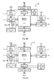
- a memory device according to one embodiment is shown in a sequence of block diagrams, designated by the general reference character 100 .
- the memory device will be referred to as a FIFO, but as will be noted below, alternate embodiments may include memory devices that process queues of data, but not necessarily in a FIFO order.
- FIG. 1A shows FIFO 100 before being programmed.
- FIG. 1B shows FIFO 100 after being programmed into one very particular configuration.
- a FIFO 100 may include a plurality of storage locations (one shown as 104 ) into which data values may be written and read in a first-in-first-out fashion.
- Storage locations e.g., 104
- queues may be related to one another, rather than operate independently of one another.
- the contents of one queue may be derived from the contents of one or more other queues.
- a FIFO 100 may be programmable into various configurations that provide functions well beyond a conventional FIFO, like that shown in FIG. 7 .
- queues may include input queues for storing input data values written into the FIFO 100 , and output queues that store output data values to be read out form the FIFO 100 .
- a functional relationship between input and output queues may be programmable. For example, data values of more than one input queue may be used to form data values for one output queue and vice versa. Multiple input queues may be merged into a smaller number of output queues, or one or more input queues may be split into a larger number of output queues. Such programmability may enable FIFO configurations having a different number of input queues than output queues. Still further, in some embodiments, an output queue may be configured to be a function (e.g., arithmetic/logic operation) of one or more input queues.
- a function e.g., arithmetic/logic operation
- a FIFO 100 may be programmable into substantially more queues than a typical conventional FIFO, including greater than 128 queues. Further, unlike a conventional FIFO (e.g., FIG. 7 ), queue depths (i.e., the number of storage locations in a queue) may be programmable, allowing queues of different sizes to be operating in the same FIFO 100 .
- FIG. 1B a FIFO 100 having one particular configuration is shown in a block diagram. It is understood that FIG. 1B is but one configuration of numerous possible configurations.
- FIFO 100 has been programmed into a configuration that includes input queues 106 - 0 to - 4 and output queues 108 - 0 to - 3 .
- a total number of input queues may be a value M
- a total number of output queues may be N, where M ⁇ N.
- output queue 108 - 0 may correspond to input queues 106 - 0 , - 1 , and - 2 . That is, input data values from input queues 106 - 0 , - 1 , - 2 may be utilized to form output data values for output queue 108 - 0 .
- Such a relationship may be conceptualized as a number of input queues (3 in this example) “merging” into a smaller number of output queues (1 in this example).
- FIG. 1B also shows the opposite case.
- Output queues 108 - 1 and - 2 may correspond to input queue 106 - 3 . That is, input data values from input queue 106 - 3 may be utilized to form output data values for both of output queues 108 - 1 and - 2 .
- Such a relationship may be conceptualized a “splitting” a number of input queues (1 in this example) into a larger number of output queues (2 in this example).
- FIG. 1B shows yet another type of relationship between input and output queues.
- Output queue 108 - 3 may correspond to input queue 106 - 4 , and thus may initially appear to operate like a conventional queue. However, values in output queue 108 - 3 may be some function of input values within input queue 106 - 4 . Such a relationship is represented in FIG. 1B by function operation 109 .
- FIG. 1B represents a logical grouping of storage locations within a FIFO 100 , and not necessarily a physical relationship between circuit elements.
- queues may be formed by pointers to physical address locations to storage locations within one or more memory arrays.
- a memory device may only physically include input queue storage locations, generating output queue values by reading from (and optionally operating on) input queue data values. In other embodiments, the reverse may be true.
- a memory device may only physically include output queue storage locations, generating output queue values by operating on input queue data values as they are read into the FIFO.
- still other embodiments may dedicate storage to both input and output queues.
- a FIFO may be configurable to provide input queues and output queues having relationships between one another.
- FIG. 1B may represent a non-programmable embodiment separate from that of FIG. 1A . That is, a FIFO 100 may be “hard-wired” to provide the illustrated functionality.
- a FIFO may be configured to include an output queue corresponding to multiple input queues. That is, an output queue may be synthesized from two or more input queues. Two particular configurations of such an arrangement are shown in FIGS. 2A and 2B .
- a FIFO configuration 200 -A may include input queues 206 - 0 , - 1 , - 2 and a corresponding output queue 208 - 0 .
- Input queues ( 206 - 0 , - 1 , - 2 ) may have equal depths, each having n+1 storage locations.
- Output queue 208 - 0 may be an arithmetic/logic function of input queues ( 206 - 0 ,- 1 ,- 2 ).
- an output queue may be an arithmetic/logic function of one or more input queues.
- a FIFO configuration 200 -B may include input queues 206 - 3 ,- 4 and a corresponding output queue 208 - 1 .
- Input queues ( 206 - 0 ,- 1 ,- 2 ) may have equal depths, each having n+1 storage locations.
- Output queue 208 - 0 may be obtained by interleaving input data values from the corresponding input queues ( 206 - 3 ,- 4 ).
- input data values from different input queues are alternated with one another.
- alternate embodiments may include different types of interleaving (e.g., alternating sequences larger than one data value, different size sequences according to input queue. etc.).
- an output queue may include interleaved data values from two or more input queues.
- a FIFO may be configured to include multiple output queues corresponding to a smaller number of input queues. That is, multiple output queues may be synthesized from a smaller number of input queues. Two particular configurations of such an arrangement are shown in FIGS. 3A and 3B .
- a FIFO configuration 300 -A may include an input queue 306 - 0 and corresponding output queues 308 - 0 , - 1 , - 2 .
- Input queue 306 - 0 may have n+1 storage locations.
- Output queues 308 - 0 , - 1 , - 2 may each be different arithmetic/logic functions of input queue 306 - 0 .
- a value “ai” is an output data value stored in position “i” of output queue 308 - 0
- “bi” is an output data value stored in position “i” of output queue 308 - 1
- “ci” is an output data value stored in position “i” of output queue 308 - 1
- “xi” is an input data value stored in position “i” of input queue 306 - 0 .
- Functions f( ), g( ) and h( ) may each be different arithmetic logic functions.
- multiple output queues may be an arithmetic/logic function of a fewer number of input queues.
- a FIFO configuration 300 -B may include input queue 306 - 1 and a corresponding output queues 308 - 3 and - 4 .
- Output queues ( 308 - 3 , - 4 ) may be obtained by “de-interleaving” input data values from the corresponding input queue 306 - 1 .
- De-interleaving may include sending some input data values of a received sequence to one output queue, while sending other input data values of the sequence to one or more other output queues.
- input data values may be sent to the two different output queues ( 308 - 3 , - 4 ) in an alternating fashion.
- interleaving operations may take various forms in the case of FIG. 2B
- de-interleaving operations may also take various other forms.
- output queues may include output data value sequences created by de-interleaving input data values from one or more input queues.
- FIGS. 2A to 3B have particularly shown one-to-many type relationships between input queues and output queues, embodiments may also include many-to-many type relationships between input and output queues. By way of illustration only, two such embodiments are shown in FIGS. 4A and 4B .
- a FIFO configuration 400 -A may include an input queues 406 - 0 , and - 1 and a corresponding output queues 408 - 0 , - 1 , - 2 .
- Input queues ( 406 - 0 ,- 1 ) may each have n+1 storage locations.
- Output queues 408 - 0 , - 1 , - 2 may each be different arithmetic/logic functions of both input queues 406 - 0 , - 1 .
- a value “ai” is an output data value stored in position “i” of output queue 408 - 0
- “bi” is an output data value stored in position “i” of output queue 408 - 1
- “ci” is an output data value stored in position “i” of output queue 408 - 2
- “xi” is an input data value stored in position “i” of input queue 406 - 0
- “yi” is an input data value stored in position “i” of input queue 406 - 1 .
- Functions f( ), g( ) and h( ) may each be different arithmetic logic functions.
- multiple output queues may be an arithmetic/logic function of a multiple input queues.
- a FIFO configuration 400 -B may include input queues 406 - 2 and - 3 and a corresponding output queues 408 - 3 and - 4 .
- Output queues ( 408 - 3 , - 4 ) may be obtained by different de-interleaving operations on input queues 406 - 2 ,- 3 .
- input queue 406 - 0 may be de-interleaved, in an alternating fashion, into even locations of output queues 408 - 3 , - 4
- input queue 406 - 1 may be de-interleaved, in an alternating fashion, into odd locations of output queues 408 - 3 , - 4 .
- other de-interleaving variations are possible.
- multiple output queues may include output data value sequences created by de-interleaving input data values from multiple input queues.
- FIGS. 2A and 2B show input queues having the same size, related input queues may have different sizes and rates to arrive at an output queue.
- FIG. 4C One particular embodiment illustrating such an arrangement is shown in FIG. 4C .
- output queue 428 - 0 may be created by interleaving values from input queue 426 - 0 at a different rate than input queue 426 - 1 .
- every fourth value may be derived from input queue 426 - 0
- the remaining values may be derived from larger input queue 426 - 1 .
- output queue sizes may differ from input queue values even in cases where interleaving does not take place.
- FIG. 4D One such embodiment is shown in FIG. 4D .
- input queues 426 - 2 and 426 - 3 may have a same size.
- output queue 428 - 1 may be three times the size, being generated by performing three different operations on each data value of the input queues 426 - 2 , - 3 .
- FIG. 4C shows input queues having variable rates and sizes
- output queues may operate in a similar fashion.
- An example of such an embodiment is shown in FIG. 4D .
- an output queue 428 - 2 may be created by operating on every other value from input queue 426 - 4 .
- output queue 428 - 3 may be created by operating on every value from input queue 426 - 4 . Consequently, output queue 428 - 2 may be smaller than output queue 428 - 3 .
- a single FIFO may be configured to include any or all of the configuration types shown above. In a very particular embodiment, such a single FIFO may be one integrated circuit device, having all circuits formed in a same integrated circuit package, or a same integrated circuit substrate.
- a QUEUE ID value may identify each possible queue of a FIFO.
- a TYPE value may define if the queue will function as an input queue or an output queue.
- a VALID value can indicate if the corresponding queue exists in the FIFO.
- a Word SIZE value may define how wide (e.g., in bits) a data word is for a queue.
- a Depth value may define how many storage locations are included within a queue.
- a SOURCE QUEUEs value may be appropriate only for output queues, and may identify those input queues used to synthesize the output queue.
- a FUNCTION value may also be appropriate for an output queue only, and may define what operations (if any) are performed on which source input queues to derive the output queue.
- configuration values may be used to define any of multiple queues and queue relationships in a programmable FIFO.
- a memory device 600 may include one or more memory arrays 610 , an input write control circuit 612 , input write control pointers 614 , an input register 616 , an output register 618 , output read control circuits 620 , output write pointers 622 , operation read pointers 624 , operation write pointers 626 , operation control logic 628 , an arithmetic logic section 630 , and a configuration data store 632 .
- Memory array(s) 610 may include memory cells addressable for read and write operations at physical addresses identified by the various pointers. Such physical addresses may correspond to particular queues as defined by configuration data 632 . Memory array(s) 610 may have single port access or multi-port access.
- Input write control circuits 612 may write data to a particular input queue based on write select values WSEL. It is understood that input read control circuits 612 may receive various other timing and control signals, as understood by those skilled in the art.
- Output read pointers 622 may indicate read locations for each output queue, as defined by configuration data 632 , and may automatically increment and wrap around as data values are read into their corresponding queues.
- An output register 618 may provide output data values read from output queues. However, in addition, output register 618 may also provide data values read from input queues in the process of generating output data values for related output queues.
- Operation control logic 628 may control actions used to create output queue data. More particularly, in response to configuration data 632 , operation control logic 628 may read input queue data values according to operation read pointers 624 . Such data values may be read into arithmetic logic circuit 630 . Based on configuration data, arithmetic logic circuits 630 may (or may not) execute predetermined operations on input data values to thereby generate output data values for corresponding output queues. Such output data values may then be written into appropriate output queue locations based on operation write pointers 626 .
- a memory device 600 may include random access circuits 611 .
- Random access circuits 611 may enable data values to be read from or written to particular locations within memory array(s) 610 . Accordingly, queue data physically stored within memory array(s) 610 may be accessed and/or operated on in a random access fashion.
- FIG. 6A shows an arrangement in which a memory device 600 may have physical storage locations for both input queues and output queues. However, as noted above, other embodiments may not physical store input queue values or output queue values. Embodiments illustrating such approaches are shown in FIGS. 6B and 6C .
- a memory device 600 ′ may include circuit sections like that of FIG. 6A .
- memory device 600 ′ may only physically store output queue values. As input values are read into the FIFO, they may be operated on by arithmetic logic section 630 to generate output values which may then be physically stored to form output queues.
- random access circuits 611 may be included to enable random access of output queue data values stored within memory array(s) 610 .
- a memory device 600 ′′ may also include circuit sections like that of FIG. 6A .
- memory device 600 ′′ may only physically store input queue values. Input values are read into the FIFO and stored to form input queues. As input data values are read out of memory device 600 ′′ they may be operated on by arithmetic logic section 630 to generate output values which may represent output queue values. Like FIGS. 6A and 6B , in some embodiments, random access circuits 611 may be included to enable random access of input queue data values stored within memory array(s) 610 .
- FIGS. 6A to 6C represent but a few of many possible embodiments, and one skilled in the art could arrive at various other circuits for implementing the memory device configurations shown above.
- embodiments may include memory devices, alternate embodiments may include data processing systems. Examples of system embodiments are shown in FIGS. 6D to 6F .
- a system 635 -D may include an interface 631 , a memory device 600 , and a processor 633 .
- An interface may 631 may receive data values, for example, from a communication network, and provide input queues to memory device 600 .
- Memory device 600 may be a memory device according to any of the embodiments shown above, or equivalents.
- a processor 633 may receive data on output queues from memory device 600 .
- a system 635 -E may include a first processor 633 - 0 that may provide input queues to memory device 600 .
- Memory device 600 may be a memory device according to any of the embodiments shown above, or equivalents.
- a processor 633 may receive data on output queues from memory device 600 .
- a system 635 -F may include a processor 633 - 0 that may provide input queues to memory device 600 and receive data on output queues from memory device 600 .
- a memory device 600 may be a memory device according to embodiments shown above, or equivalents.
- the various memory device configurations shown in the embodiments may not be programmable, but rather have input to output queue relationships determined by circuits with a set functionality.
- Embodiments of the invention that provide for programmable queue depths may allow for optimal use of memory device density. This is in contrast to conventional approaches with fixed queue sizes that may unnecessarily include extra locations in a queue pipeline.
- Embodiments of the invention that provide for interrelated queues may decrease bandwidth requirement and/or latency in a system.
- some applications may require switching between different queues, which may increase access times.
- a FIFO according to embodiments may present data from multiple queues at the same time, by interleaving and/or queue splitting as described above, and equivalents.
- Embodiments of the invention may increase system bandwidth and computation resources over conventional approaches.
- Embodiments that perform arithmetic logic operations on input data streams to form output queues may save computation resources of a processor in the system, effectively “pre-computing” results on entire data streams.
- a processor would have to execute a computation for each data value read from multiple FIFO queues.
- Embodiments of the invention may increase flexibility in a system.
- a FIFO may be configured to generate multiple output queues from one input queue.
- Such an arrangement may allow access to such input data values in multiple ways before such values are overwritten with new input data. This is in contrast to a conventional approach in which multiple processes would have to arbitrate access to a same queue.
- Embodiments of the invention may be included in numerous applications.
- a FIFO may be included in data packet processing devices, such as base stations.
- Such processing devices may process packets differently according to some criteria, such as quality of service (QoS), as but one example. Packets arriving on one input queue may be sent to different output queues based on a QoS value of the packet.
- QoS quality of service
- Packets arriving on one input queue may be sent to different output queues based on a QoS value of the packet.
- a visible frame may present image data from two different sources (e.g., picture-in-picture) or area-of-interest (AOI). Video data on two different input queues may be merged into a single output queue.
- sources e.g., picture-in-picture
- AOI area-of-interest
Abstract
Description
ai=f(xi,yi,zi)
where “ai” is an output data value stored in position “i” of output queue 208-0, “xi” is an input data value stored in position “i” of input queue 206-0, “yi” is an input data value stored in position “i” of input queue 206-1, “zi” is an input data value stored in position “i” of input queue 206-2, and f( ) is an arithmetic logic function.
Claims (22)
Priority Applications (1)
| Application Number | Priority Date | Filing Date | Title |
|---|---|---|---|
| US12/900,283 US9465576B1 (en) | 2009-10-07 | 2010-10-07 | First-in-first-out (FIFO) memory devices and methods having multiple queuing |
Applications Claiming Priority (2)
| Application Number | Priority Date | Filing Date | Title |
|---|---|---|---|
| US24957709P | 2009-10-07 | 2009-10-07 | |
| US12/900,283 US9465576B1 (en) | 2009-10-07 | 2010-10-07 | First-in-first-out (FIFO) memory devices and methods having multiple queuing |
Publications (1)
| Publication Number | Publication Date |
|---|---|
| US9465576B1 true US9465576B1 (en) | 2016-10-11 |
Family
ID=57046615
Family Applications (1)
| Application Number | Title | Priority Date | Filing Date |
|---|---|---|---|
| US12/900,283 Active 2032-05-19 US9465576B1 (en) | 2009-10-07 | 2010-10-07 | First-in-first-out (FIFO) memory devices and methods having multiple queuing |
Country Status (1)
| Country | Link |
|---|---|
| US (1) | US9465576B1 (en) |
Citations (16)
| Publication number | Priority date | Publication date | Assignee | Title |
|---|---|---|---|---|
| US5519701A (en) | 1995-03-29 | 1996-05-21 | International Business Machines Corporation | Architecture for high performance management of multiple circular FIFO storage means |
| US5901291A (en) | 1996-10-21 | 1999-05-04 | International Business Machines Corporation | Method and apparatus for maintaining message order in multi-user FIFO stacks |
| US6292491B1 (en) | 1998-08-25 | 2001-09-18 | Cisco Technology, Inc. | Distributed FIFO queuing for ATM systems |
| US6430156B1 (en) | 1997-12-31 | 2002-08-06 | Hyundai Electronics Inds Co Ltd. | Traffic control method for providing predictive guaranteed service |
| US6526495B1 (en) * | 2000-03-22 | 2003-02-25 | Cypress Semiconductor Corp. | Multiport FIFO with programmable width and depth |
| US6538467B2 (en) | 2001-08-20 | 2003-03-25 | Micron Technology, Inc. | Multi-access FIFO queue |
| US6564309B1 (en) * | 1998-04-09 | 2003-05-13 | Stmicroelectronics S.A. | DSP architecture optimized for memory accesses |
| US6684317B2 (en) * | 2001-12-21 | 2004-01-27 | Axiowave Networks, Inc. | Method of addressing sequential data packets from a plurality of input data line cards for shared memory storage and the like, and novel address generator therefor |
| US6892199B2 (en) | 2001-06-29 | 2005-05-10 | Trendium, Inc. | Saving burst data by using semi-merge sorting module |
| US6907479B2 (en) * | 2001-07-18 | 2005-06-14 | Integrated Device Technology, Inc. | Integrated circuit FIFO memory devices that are divisible into independent FIFO queues, and systems and methods for controlling same |
| US7120075B1 (en) * | 2003-08-18 | 2006-10-10 | Integrated Device Technology, Inc. | Multi-FIFO integrated circuit devices that support multi-queue operating modes with enhanced write path and read path queue switching |
| US7257687B2 (en) * | 2004-07-26 | 2007-08-14 | Integrated Device Technology, Inc. | Synchronization of active flag and status bus flags in a multi-queue first-in first-out memory system |
| US20090086748A1 (en) | 2007-09-27 | 2009-04-02 | Integrated Device Technology, Inc. | Multi-Function Queue To Support Data Offload, Protocol Translation And Pass-Through FIFO |
| US7668187B2 (en) * | 2002-05-16 | 2010-02-23 | Topside Research, Llc | Method for reordering sequenced packets |
| US8559439B1 (en) * | 2010-11-03 | 2013-10-15 | Pmc-Sierra Us, Inc. | Method and apparatus for queue ordering in a multi-engine processing system |
| US8571048B2 (en) * | 2007-04-30 | 2013-10-29 | Hewlett-Packard Development Company, L.P. | Dynamic memory queue depth algorithm |
-
2010
- 2010-10-07 US US12/900,283 patent/US9465576B1/en active Active
Patent Citations (16)
| Publication number | Priority date | Publication date | Assignee | Title |
|---|---|---|---|---|
| US5519701A (en) | 1995-03-29 | 1996-05-21 | International Business Machines Corporation | Architecture for high performance management of multiple circular FIFO storage means |
| US5901291A (en) | 1996-10-21 | 1999-05-04 | International Business Machines Corporation | Method and apparatus for maintaining message order in multi-user FIFO stacks |
| US6430156B1 (en) | 1997-12-31 | 2002-08-06 | Hyundai Electronics Inds Co Ltd. | Traffic control method for providing predictive guaranteed service |
| US6564309B1 (en) * | 1998-04-09 | 2003-05-13 | Stmicroelectronics S.A. | DSP architecture optimized for memory accesses |
| US6292491B1 (en) | 1998-08-25 | 2001-09-18 | Cisco Technology, Inc. | Distributed FIFO queuing for ATM systems |
| US6526495B1 (en) * | 2000-03-22 | 2003-02-25 | Cypress Semiconductor Corp. | Multiport FIFO with programmable width and depth |
| US6892199B2 (en) | 2001-06-29 | 2005-05-10 | Trendium, Inc. | Saving burst data by using semi-merge sorting module |
| US6907479B2 (en) * | 2001-07-18 | 2005-06-14 | Integrated Device Technology, Inc. | Integrated circuit FIFO memory devices that are divisible into independent FIFO queues, and systems and methods for controlling same |
| US6538467B2 (en) | 2001-08-20 | 2003-03-25 | Micron Technology, Inc. | Multi-access FIFO queue |
| US6684317B2 (en) * | 2001-12-21 | 2004-01-27 | Axiowave Networks, Inc. | Method of addressing sequential data packets from a plurality of input data line cards for shared memory storage and the like, and novel address generator therefor |
| US7668187B2 (en) * | 2002-05-16 | 2010-02-23 | Topside Research, Llc | Method for reordering sequenced packets |
| US7120075B1 (en) * | 2003-08-18 | 2006-10-10 | Integrated Device Technology, Inc. | Multi-FIFO integrated circuit devices that support multi-queue operating modes with enhanced write path and read path queue switching |
| US7257687B2 (en) * | 2004-07-26 | 2007-08-14 | Integrated Device Technology, Inc. | Synchronization of active flag and status bus flags in a multi-queue first-in first-out memory system |
| US8571048B2 (en) * | 2007-04-30 | 2013-10-29 | Hewlett-Packard Development Company, L.P. | Dynamic memory queue depth algorithm |
| US20090086748A1 (en) | 2007-09-27 | 2009-04-02 | Integrated Device Technology, Inc. | Multi-Function Queue To Support Data Offload, Protocol Translation And Pass-Through FIFO |
| US8559439B1 (en) * | 2010-11-03 | 2013-10-15 | Pmc-Sierra Us, Inc. | Method and apparatus for queue ordering in a multi-engine processing system |
Non-Patent Citations (3)
| Title |
|---|
| "Interfacing the IDT 3.3V Multi-Queue FIFO to a Virtex-II FPGA",http://www.xilinx.com/support/documentation/application-notes/xapp629.pdf. |
| "Maximum I/O Flexibility for RTL-like Performance", http://www.tensilica.com/products/xtensa-customizable/xtensa-lx2/i-o-bandwidth.htm. |
| Mondrian Nüssle, Benjamin Geib, Holger Fröning, Ulrich Bröning, "An FPGA-based custom high performance interconnection network"; http://ra.ziti.uni-heidelberg.de/pages/publications/papers/2009/7.pdf. |
Similar Documents
| Publication | Publication Date | Title |
|---|---|---|
| US10749528B2 (en) | Stacked programmable integrated circuitry with smart memory | |
| EP3149595B1 (en) | Systems and methods for segmenting data structures in a memory system | |
| KR100663248B1 (en) | Simultaneous addressing using single-port rams | |
| US9342479B2 (en) | Systems and methods of data extraction in a vector processor | |
| US7555579B2 (en) | Implementing FIFOs in shared memory using linked lists and interleaved linked lists | |
| JP6535253B2 (en) | Method and apparatus for utilizing multiple linked memory lists | |
| US9705505B2 (en) | Reconfigurable semiconductor device | |
| US7439763B1 (en) | Scalable shared network memory switch for an FPGA | |
| US20190332313A1 (en) | Data buffer processing method and data buffer processing system for 4r4w fully-shared packet | |
| US20050091465A1 (en) | FIFO memory with single port memory modules for allowing simultaneous read and write operations | |
| KR20140085467A (en) | Shiftable memory employing ring registers | |
| EP1811370A2 (en) | A first-in first-out (FIFO) memory architecture providing multiport functionality | |
| US10319418B2 (en) | Methods and systems for parallel column twist interleaving | |
| US8862836B2 (en) | Multi-port register file with an input pipelined architecture with asynchronous reads and localized feedback | |
| CN111566614B (en) | Bit width matching circuit, data writing device, data reading device, and electronic apparatus | |
| US7568074B1 (en) | Time based data storage for shared network memory switch | |
| US9465576B1 (en) | First-in-first-out (FIFO) memory devices and methods having multiple queuing | |
| US9478272B1 (en) | Configurable storage blocks with embedded first-in first-out and last-in first-out circuitry | |
| US9715343B2 (en) | Multidimensional partitioned storage array and method utilizing input shifters to allow multiple entire columns or rows to be accessed in a single clock cycle | |
| US9304899B1 (en) | Network interface circuitry with flexible memory addressing capabilities | |
| EP3255635A1 (en) | Emulated multiport memory element circuitry | |
| US7730276B1 (en) | Striping of data into memory of a network data switch to prevent read and write collisions | |
| US9367450B1 (en) | Address arithmetic on block RAMs | |
| JP5499131B2 (en) | Dual port memory and method thereof | |
| US10102892B1 (en) | RAM-based shift register with embedded addressing |
Legal Events
| Date | Code | Title | Description |
|---|---|---|---|
| AS | Assignment |
Owner name: CYPRESS SEMICONDUCTOR CORPORATION, CALIFORNIA Free format text: ASSIGNMENT OF ASSIGNORS INTEREST;ASSIGNOR:MAHESHWARI, DINESH;REEL/FRAME:025110/0093 Effective date: 20101007 |
|
| AS | Assignment |
Owner name: MORGAN STANLEY SENIOR FUNDING, INC., NEW YORK Free format text: SECURITY INTEREST;ASSIGNORS:CYPRESS SEMICONDUCTOR CORPORATION;SPANSION LLC;REEL/FRAME:035240/0429 Effective date: 20150312 |
|
| STCF | Information on status: patent grant |
Free format text: PATENTED CASE |
|
| AS | Assignment |
Owner name: MUFG UNION BANK, N.A., CALIFORNIA Free format text: ASSIGNMENT AND ASSUMPTION OF SECURITY INTEREST IN INTELLECTUAL PROPERTY;ASSIGNOR:MORGAN STANLEY SENIOR FUNDING, INC.;REEL/FRAME:050896/0366 Effective date: 20190731 |
|
| MAFP | Maintenance fee payment |
Free format text: PAYMENT OF MAINTENANCE FEE, 4TH YEAR, LARGE ENTITY (ORIGINAL EVENT CODE: M1551); ENTITY STATUS OF PATENT OWNER: LARGE ENTITY Year of fee payment: 4 |
|
| AS | Assignment |
Owner name: MORGAN STANLEY SENIOR FUNDING, INC., NEW YORK Free format text: CORRECTIVE ASSIGNMENT TO CORRECT THE 8647899 PREVIOUSLY RECORDED ON REEL 035240 FRAME 0429. ASSIGNOR(S) HEREBY CONFIRMS THE SECURITY INTERST;ASSIGNORS:CYPRESS SEMICONDUCTOR CORPORATION;SPANSION LLC;REEL/FRAME:058002/0470 Effective date: 20150312 |
|
| AS | Assignment |
Owner name: SPANSION LLC, CALIFORNIA Free format text: RELEASE BY SECURED PARTY;ASSIGNOR:MUFG UNION BANK, N.A.;REEL/FRAME:059410/0438 Effective date: 20200416 Owner name: CYPRESS SEMICONDUCTOR CORPORATION, CALIFORNIA Free format text: RELEASE BY SECURED PARTY;ASSIGNOR:MUFG UNION BANK, N.A.;REEL/FRAME:059410/0438 Effective date: 20200416 |