US9460376B2 - Radio IC device - Google Patents
Radio IC device Download PDFInfo
- Publication number
- US9460376B2 US9460376B2 US12/688,072 US68807210A US9460376B2 US 9460376 B2 US9460376 B2 US 9460376B2 US 68807210 A US68807210 A US 68807210A US 9460376 B2 US9460376 B2 US 9460376B2
- Authority
- US
- United States
- Prior art keywords
- radio
- preferred
- electrode
- feed circuit
- radiation plate
- Prior art date
- Legal status (The legal status is an assumption and is not a legal conclusion. Google has not performed a legal analysis and makes no representation as to the accuracy of the status listed.)
- Active, expires
Links
- 230000008878 coupling Effects 0.000 claims abstract description 118
- 238000010168 coupling process Methods 0.000 claims abstract description 118
- 238000005859 coupling reaction Methods 0.000 claims abstract description 118
- 230000005855 radiation Effects 0.000 claims abstract description 108
- 239000002184 metal Substances 0.000 claims abstract description 58
- 229910052751 metal Inorganic materials 0.000 claims abstract description 58
- 238000000034 method Methods 0.000 claims abstract description 7
- 230000008569 process Effects 0.000 claims abstract description 6
- 239000000758 substrate Substances 0.000 claims description 22
- 239000000919 ceramic Substances 0.000 claims description 6
- 239000011347 resin Substances 0.000 claims description 4
- 229920005989 resin Polymers 0.000 claims description 4
- 230000006870 function Effects 0.000 abstract description 56
- 239000004020 conductor Substances 0.000 description 47
- 230000000694 effects Effects 0.000 description 31
- 239000003990 capacitor Substances 0.000 description 18
- 229910000679 solder Inorganic materials 0.000 description 6
- 238000013461 design Methods 0.000 description 5
- 239000000463 material Substances 0.000 description 5
- 239000000853 adhesive Substances 0.000 description 4
- 230000001070 adhesive effect Effects 0.000 description 4
- 238000004891 communication Methods 0.000 description 4
- 230000004048 modification Effects 0.000 description 4
- 238000012986 modification Methods 0.000 description 4
- 238000004806 packaging method and process Methods 0.000 description 4
- 230000015572 biosynthetic process Effects 0.000 description 3
- 230000008859 change Effects 0.000 description 3
- 230000005684 electric field Effects 0.000 description 3
- 238000004519 manufacturing process Methods 0.000 description 3
- 229920000106 Liquid crystal polymer Polymers 0.000 description 2
- 239000004977 Liquid-crystal polymers (LCPs) Substances 0.000 description 2
- 230000008901 benefit Effects 0.000 description 2
- 230000001413 cellular effect Effects 0.000 description 2
- 239000012811 non-conductive material Substances 0.000 description 2
- 230000008054 signal transmission Effects 0.000 description 2
- 229920002799 BoPET Polymers 0.000 description 1
- 239000004642 Polyimide Substances 0.000 description 1
- 229910010293 ceramic material Inorganic materials 0.000 description 1
- 239000002131 composite material Substances 0.000 description 1
- 230000000593 degrading effect Effects 0.000 description 1
- 238000010586 diagram Methods 0.000 description 1
- 239000003989 dielectric material Substances 0.000 description 1
- 238000010304 firing Methods 0.000 description 1
- 230000004907 flux Effects 0.000 description 1
- 229910052737 gold Inorganic materials 0.000 description 1
- 230000006698 induction Effects 0.000 description 1
- 239000004973 liquid crystal related substance Substances 0.000 description 1
- 239000002923 metal particle Substances 0.000 description 1
- 238000012856 packing Methods 0.000 description 1
- 210000003254 palate Anatomy 0.000 description 1
- 229920001721 polyimide Polymers 0.000 description 1
- 238000003825 pressing Methods 0.000 description 1
- 238000007639 printing Methods 0.000 description 1
- 238000012545 processing Methods 0.000 description 1
- 230000001681 protective effect Effects 0.000 description 1
- 239000011241 protective layer Substances 0.000 description 1
- 230000009467 reduction Effects 0.000 description 1
- 229910052709 silver Inorganic materials 0.000 description 1
- 238000005476 soldering Methods 0.000 description 1
- 238000012546 transfer Methods 0.000 description 1
Images


Classifications
-
- G—PHYSICS
- G06—COMPUTING; CALCULATING OR COUNTING
- G06K—GRAPHICAL DATA READING; PRESENTATION OF DATA; RECORD CARRIERS; HANDLING RECORD CARRIERS
- G06K19/00—Record carriers for use with machines and with at least a part designed to carry digital markings
- G06K19/06—Record carriers for use with machines and with at least a part designed to carry digital markings characterised by the kind of the digital marking, e.g. shape, nature, code
- G06K19/067—Record carriers with conductive marks, printed circuits or semiconductor circuit elements, e.g. credit or identity cards also with resonating or responding marks without active components
- G06K19/07—Record carriers with conductive marks, printed circuits or semiconductor circuit elements, e.g. credit or identity cards also with resonating or responding marks without active components with integrated circuit chips
- G06K19/077—Constructional details, e.g. mounting of circuits in the carrier
- G06K19/07749—Constructional details, e.g. mounting of circuits in the carrier the record carrier being capable of non-contact communication, e.g. constructional details of the antenna of a non-contact smart card
-
- G—PHYSICS
- G06—COMPUTING; CALCULATING OR COUNTING
- G06K—GRAPHICAL DATA READING; PRESENTATION OF DATA; RECORD CARRIERS; HANDLING RECORD CARRIERS
- G06K19/00—Record carriers for use with machines and with at least a part designed to carry digital markings
- G06K19/06—Record carriers for use with machines and with at least a part designed to carry digital markings characterised by the kind of the digital marking, e.g. shape, nature, code
- G06K19/06187—Record carriers for use with machines and with at least a part designed to carry digital markings characterised by the kind of the digital marking, e.g. shape, nature, code with magnetically detectable marking
-
- G—PHYSICS
- G06—COMPUTING; CALCULATING OR COUNTING
- G06K—GRAPHICAL DATA READING; PRESENTATION OF DATA; RECORD CARRIERS; HANDLING RECORD CARRIERS
- G06K19/00—Record carriers for use with machines and with at least a part designed to carry digital markings
- G06K19/06—Record carriers for use with machines and with at least a part designed to carry digital markings characterised by the kind of the digital marking, e.g. shape, nature, code
- G06K19/067—Record carriers with conductive marks, printed circuits or semiconductor circuit elements, e.g. credit or identity cards also with resonating or responding marks without active components
- G06K19/07—Record carriers with conductive marks, printed circuits or semiconductor circuit elements, e.g. credit or identity cards also with resonating or responding marks without active components with integrated circuit chips
- G06K19/0723—Record carriers with conductive marks, printed circuits or semiconductor circuit elements, e.g. credit or identity cards also with resonating or responding marks without active components with integrated circuit chips the record carrier comprising an arrangement for non-contact communication, e.g. wireless communication circuits on transponder cards, non-contact smart cards or RFIDs
-
- G—PHYSICS
- G06—COMPUTING; CALCULATING OR COUNTING
- G06K—GRAPHICAL DATA READING; PRESENTATION OF DATA; RECORD CARRIERS; HANDLING RECORD CARRIERS
- G06K19/00—Record carriers for use with machines and with at least a part designed to carry digital markings
- G06K19/06—Record carriers for use with machines and with at least a part designed to carry digital markings characterised by the kind of the digital marking, e.g. shape, nature, code
- G06K19/067—Record carriers with conductive marks, printed circuits or semiconductor circuit elements, e.g. credit or identity cards also with resonating or responding marks without active components
- G06K19/07—Record carriers with conductive marks, printed circuits or semiconductor circuit elements, e.g. credit or identity cards also with resonating or responding marks without active components with integrated circuit chips
- G06K19/077—Constructional details, e.g. mounting of circuits in the carrier
- G06K19/07749—Constructional details, e.g. mounting of circuits in the carrier the record carrier being capable of non-contact communication, e.g. constructional details of the antenna of a non-contact smart card
- G06K19/0775—Constructional details, e.g. mounting of circuits in the carrier the record carrier being capable of non-contact communication, e.g. constructional details of the antenna of a non-contact smart card arrangements for connecting the integrated circuit to the antenna
- G06K19/07756—Constructional details, e.g. mounting of circuits in the carrier the record carrier being capable of non-contact communication, e.g. constructional details of the antenna of a non-contact smart card arrangements for connecting the integrated circuit to the antenna the connection being non-galvanic, e.g. capacitive
-
- G—PHYSICS
- G06—COMPUTING; CALCULATING OR COUNTING
- G06K—GRAPHICAL DATA READING; PRESENTATION OF DATA; RECORD CARRIERS; HANDLING RECORD CARRIERS
- G06K19/00—Record carriers for use with machines and with at least a part designed to carry digital markings
- G06K19/06—Record carriers for use with machines and with at least a part designed to carry digital markings characterised by the kind of the digital marking, e.g. shape, nature, code
- G06K19/067—Record carriers with conductive marks, printed circuits or semiconductor circuit elements, e.g. credit or identity cards also with resonating or responding marks without active components
- G06K19/07—Record carriers with conductive marks, printed circuits or semiconductor circuit elements, e.g. credit or identity cards also with resonating or responding marks without active components with integrated circuit chips
- G06K19/077—Constructional details, e.g. mounting of circuits in the carrier
- G06K19/07749—Constructional details, e.g. mounting of circuits in the carrier the record carrier being capable of non-contact communication, e.g. constructional details of the antenna of a non-contact smart card
- G06K19/07773—Antenna details
- G06K19/07777—Antenna details the antenna being of the inductive type
- G06K19/07779—Antenna details the antenna being of the inductive type the inductive antenna being a coil
- G06K19/07783—Antenna details the antenna being of the inductive type the inductive antenna being a coil the coil being planar
-
- G—PHYSICS
- G06—COMPUTING; CALCULATING OR COUNTING
- G06K—GRAPHICAL DATA READING; PRESENTATION OF DATA; RECORD CARRIERS; HANDLING RECORD CARRIERS
- G06K19/00—Record carriers for use with machines and with at least a part designed to carry digital markings
- G06K19/06—Record carriers for use with machines and with at least a part designed to carry digital markings characterised by the kind of the digital marking, e.g. shape, nature, code
- G06K19/067—Record carriers with conductive marks, printed circuits or semiconductor circuit elements, e.g. credit or identity cards also with resonating or responding marks without active components
- G06K19/07—Record carriers with conductive marks, printed circuits or semiconductor circuit elements, e.g. credit or identity cards also with resonating or responding marks without active components with integrated circuit chips
- G06K19/077—Constructional details, e.g. mounting of circuits in the carrier
- G06K19/07749—Constructional details, e.g. mounting of circuits in the carrier the record carrier being capable of non-contact communication, e.g. constructional details of the antenna of a non-contact smart card
- G06K19/07773—Antenna details
- G06K19/07777—Antenna details the antenna being of the inductive type
- G06K19/07784—Antenna details the antenna being of the inductive type the inductive antenna consisting of a plurality of coils stacked on top of one another
-
- G—PHYSICS
- G06—COMPUTING; CALCULATING OR COUNTING
- G06K—GRAPHICAL DATA READING; PRESENTATION OF DATA; RECORD CARRIERS; HANDLING RECORD CARRIERS
- G06K19/00—Record carriers for use with machines and with at least a part designed to carry digital markings
- G06K19/06—Record carriers for use with machines and with at least a part designed to carry digital markings characterised by the kind of the digital marking, e.g. shape, nature, code
- G06K19/067—Record carriers with conductive marks, printed circuits or semiconductor circuit elements, e.g. credit or identity cards also with resonating or responding marks without active components
- G06K19/07—Record carriers with conductive marks, printed circuits or semiconductor circuit elements, e.g. credit or identity cards also with resonating or responding marks without active components with integrated circuit chips
- G06K19/077—Constructional details, e.g. mounting of circuits in the carrier
- G06K19/07749—Constructional details, e.g. mounting of circuits in the carrier the record carrier being capable of non-contact communication, e.g. constructional details of the antenna of a non-contact smart card
- G06K19/07773—Antenna details
- G06K19/07786—Antenna details the antenna being of the HF type, such as a dipole
-
- H—ELECTRICITY
- H01—ELECTRIC ELEMENTS
- H01L—SEMICONDUCTOR DEVICES NOT COVERED BY CLASS H10
- H01L23/00—Details of semiconductor or other solid state devices
- H01L23/48—Arrangements for conducting electric current to or from the solid state body in operation, e.g. leads, terminal arrangements ; Selection of materials therefor
- H01L23/488—Arrangements for conducting electric current to or from the solid state body in operation, e.g. leads, terminal arrangements ; Selection of materials therefor consisting of soldered or bonded constructions
- H01L23/498—Leads, i.e. metallisations or lead-frames on insulating substrates, e.g. chip carriers
- H01L23/49838—Geometry or layout
-
- H—ELECTRICITY
- H01—ELECTRIC ELEMENTS
- H01L—SEMICONDUCTOR DEVICES NOT COVERED BY CLASS H10
- H01L23/00—Details of semiconductor or other solid state devices
- H01L23/552—Protection against radiation, e.g. light or electromagnetic waves
-
- H—ELECTRICITY
- H01—ELECTRIC ELEMENTS
- H01L—SEMICONDUCTOR DEVICES NOT COVERED BY CLASS H10
- H01L23/00—Details of semiconductor or other solid state devices
- H01L23/58—Structural electrical arrangements for semiconductor devices not otherwise provided for, e.g. in combination with batteries
- H01L23/64—Impedance arrangements
- H01L23/66—High-frequency adaptations
-
- H—ELECTRICITY
- H01—ELECTRIC ELEMENTS
- H01Q—ANTENNAS, i.e. RADIO AERIALS
- H01Q1/00—Details of, or arrangements associated with, antennas
- H01Q1/36—Structural form of radiating elements, e.g. cone, spiral, umbrella; Particular materials used therewith
-
- H—ELECTRICITY
- H01—ELECTRIC ELEMENTS
- H01Q—ANTENNAS, i.e. RADIO AERIALS
- H01Q1/00—Details of, or arrangements associated with, antennas
- H01Q1/36—Structural form of radiating elements, e.g. cone, spiral, umbrella; Particular materials used therewith
- H01Q1/38—Structural form of radiating elements, e.g. cone, spiral, umbrella; Particular materials used therewith formed by a conductive layer on an insulating support
-
- H—ELECTRICITY
- H01—ELECTRIC ELEMENTS
- H01Q—ANTENNAS, i.e. RADIO AERIALS
- H01Q1/00—Details of, or arrangements associated with, antennas
- H01Q1/42—Housings not intimately mechanically associated with radiating elements, e.g. radome
-
- H—ELECTRICITY
- H01—ELECTRIC ELEMENTS
- H01Q—ANTENNAS, i.e. RADIO AERIALS
- H01Q1/00—Details of, or arrangements associated with, antennas
- H01Q1/44—Details of, or arrangements associated with, antennas using equipment having another main function to serve additionally as an antenna, e.g. means for giving an antenna an aesthetic aspect
-
- H—ELECTRICITY
- H01—ELECTRIC ELEMENTS
- H01Q—ANTENNAS, i.e. RADIO AERIALS
- H01Q13/00—Waveguide horns or mouths; Slot antennas; Leaky-waveguide antennas; Equivalent structures causing radiation along the transmission path of a guided wave
- H01Q13/10—Resonant slot antennas
-
- H—ELECTRICITY
- H01—ELECTRIC ELEMENTS
- H01Q—ANTENNAS, i.e. RADIO AERIALS
- H01Q7/00—Loop antennas with a substantially uniform current distribution around the loop and having a directional radiation pattern in a plane perpendicular to the plane of the loop
-
- H—ELECTRICITY
- H01—ELECTRIC ELEMENTS
- H01Q—ANTENNAS, i.e. RADIO AERIALS
- H01Q9/00—Electrically-short antennas having dimensions not more than twice the operating wavelength and consisting of conductive active radiating elements
- H01Q9/04—Resonant antennas
- H01Q9/16—Resonant antennas with feed intermediate between the extremities of the antenna, e.g. centre-fed dipole
-
- H—ELECTRICITY
- H01—ELECTRIC ELEMENTS
- H01Q—ANTENNAS, i.e. RADIO AERIALS
- H01Q9/00—Electrically-short antennas having dimensions not more than twice the operating wavelength and consisting of conductive active radiating elements
- H01Q9/04—Resonant antennas
- H01Q9/30—Resonant antennas with feed to end of elongated active element, e.g. unipole
-
- H—ELECTRICITY
- H05—ELECTRIC TECHNIQUES NOT OTHERWISE PROVIDED FOR
- H05K—PRINTED CIRCUITS; CASINGS OR CONSTRUCTIONAL DETAILS OF ELECTRIC APPARATUS; MANUFACTURE OF ASSEMBLAGES OF ELECTRICAL COMPONENTS
- H05K1/00—Printed circuits
- H05K1/02—Details
- H05K1/0213—Electrical arrangements not otherwise provided for
- H05K1/0216—Reduction of cross-talk, noise or electromagnetic interference
-
- H—ELECTRICITY
- H05—ELECTRIC TECHNIQUES NOT OTHERWISE PROVIDED FOR
- H05K—PRINTED CIRCUITS; CASINGS OR CONSTRUCTIONAL DETAILS OF ELECTRIC APPARATUS; MANUFACTURE OF ASSEMBLAGES OF ELECTRICAL COMPONENTS
- H05K1/00—Printed circuits
- H05K1/02—Details
- H05K1/14—Structural association of two or more printed circuits
- H05K1/141—One or more single auxiliary printed circuits mounted on a main printed circuit, e.g. modules, adapters
-
- H—ELECTRICITY
- H05—ELECTRIC TECHNIQUES NOT OTHERWISE PROVIDED FOR
- H05K—PRINTED CIRCUITS; CASINGS OR CONSTRUCTIONAL DETAILS OF ELECTRIC APPARATUS; MANUFACTURE OF ASSEMBLAGES OF ELECTRICAL COMPONENTS
- H05K1/00—Printed circuits
- H05K1/18—Printed circuits structurally associated with non-printed electric components
- H05K1/181—Printed circuits structurally associated with non-printed electric components associated with surface mounted components
-
- H—ELECTRICITY
- H01—ELECTRIC ELEMENTS
- H01L—SEMICONDUCTOR DEVICES NOT COVERED BY CLASS H10
- H01L2223/00—Details relating to semiconductor or other solid state devices covered by the group H01L23/00
- H01L2223/58—Structural electrical arrangements for semiconductor devices not otherwise provided for
- H01L2223/64—Impedance arrangements
- H01L2223/66—High-frequency adaptations
- H01L2223/6644—Packaging aspects of high-frequency amplifiers
- H01L2223/6655—Matching arrangements, e.g. arrangement of inductive and capacitive components
-
- H—ELECTRICITY
- H01—ELECTRIC ELEMENTS
- H01L—SEMICONDUCTOR DEVICES NOT COVERED BY CLASS H10
- H01L2223/00—Details relating to semiconductor or other solid state devices covered by the group H01L23/00
- H01L2223/58—Structural electrical arrangements for semiconductor devices not otherwise provided for
- H01L2223/64—Impedance arrangements
- H01L2223/66—High-frequency adaptations
- H01L2223/6661—High-frequency adaptations for passive devices
- H01L2223/6677—High-frequency adaptations for passive devices for antenna, e.g. antenna included within housing of semiconductor device
-
- H—ELECTRICITY
- H01—ELECTRIC ELEMENTS
- H01L—SEMICONDUCTOR DEVICES NOT COVERED BY CLASS H10
- H01L2224/00—Indexing scheme for arrangements for connecting or disconnecting semiconductor or solid-state bodies and methods related thereto as covered by H01L24/00
- H01L2224/01—Means for bonding being attached to, or being formed on, the surface to be connected, e.g. chip-to-package, die-attach, "first-level" interconnects; Manufacturing methods related thereto
- H01L2224/10—Bump connectors; Manufacturing methods related thereto
- H01L2224/15—Structure, shape, material or disposition of the bump connectors after the connecting process
- H01L2224/16—Structure, shape, material or disposition of the bump connectors after the connecting process of an individual bump connector
- H01L2224/161—Disposition
- H01L2224/16151—Disposition the bump connector connecting between a semiconductor or solid-state body and an item not being a semiconductor or solid-state body, e.g. chip-to-substrate, chip-to-passive
- H01L2224/16221—Disposition the bump connector connecting between a semiconductor or solid-state body and an item not being a semiconductor or solid-state body, e.g. chip-to-substrate, chip-to-passive the body and the item being stacked
- H01L2224/16225—Disposition the bump connector connecting between a semiconductor or solid-state body and an item not being a semiconductor or solid-state body, e.g. chip-to-substrate, chip-to-passive the body and the item being stacked the item being non-metallic, e.g. insulating substrate with or without metallisation
- H01L2224/16227—Disposition the bump connector connecting between a semiconductor or solid-state body and an item not being a semiconductor or solid-state body, e.g. chip-to-substrate, chip-to-passive the body and the item being stacked the item being non-metallic, e.g. insulating substrate with or without metallisation the bump connector connecting to a bond pad of the item
-
- H—ELECTRICITY
- H01—ELECTRIC ELEMENTS
- H01L—SEMICONDUCTOR DEVICES NOT COVERED BY CLASS H10
- H01L2224/00—Indexing scheme for arrangements for connecting or disconnecting semiconductor or solid-state bodies and methods related thereto as covered by H01L24/00
- H01L2224/01—Means for bonding being attached to, or being formed on, the surface to be connected, e.g. chip-to-package, die-attach, "first-level" interconnects; Manufacturing methods related thereto
- H01L2224/26—Layer connectors, e.g. plate connectors, solder or adhesive layers; Manufacturing methods related thereto
- H01L2224/31—Structure, shape, material or disposition of the layer connectors after the connecting process
- H01L2224/32—Structure, shape, material or disposition of the layer connectors after the connecting process of an individual layer connector
- H01L2224/321—Disposition
- H01L2224/32151—Disposition the layer connector connecting between a semiconductor or solid-state body and an item not being a semiconductor or solid-state body, e.g. chip-to-substrate, chip-to-passive
- H01L2224/32221—Disposition the layer connector connecting between a semiconductor or solid-state body and an item not being a semiconductor or solid-state body, e.g. chip-to-substrate, chip-to-passive the body and the item being stacked
- H01L2224/32225—Disposition the layer connector connecting between a semiconductor or solid-state body and an item not being a semiconductor or solid-state body, e.g. chip-to-substrate, chip-to-passive the body and the item being stacked the item being non-metallic, e.g. insulating substrate with or without metallisation
-
- H—ELECTRICITY
- H01—ELECTRIC ELEMENTS
- H01L—SEMICONDUCTOR DEVICES NOT COVERED BY CLASS H10
- H01L2224/00—Indexing scheme for arrangements for connecting or disconnecting semiconductor or solid-state bodies and methods related thereto as covered by H01L24/00
- H01L2224/01—Means for bonding being attached to, or being formed on, the surface to be connected, e.g. chip-to-package, die-attach, "first-level" interconnects; Manufacturing methods related thereto
- H01L2224/42—Wire connectors; Manufacturing methods related thereto
- H01L2224/47—Structure, shape, material or disposition of the wire connectors after the connecting process
- H01L2224/48—Structure, shape, material or disposition of the wire connectors after the connecting process of an individual wire connector
- H01L2224/4805—Shape
- H01L2224/4809—Loop shape
- H01L2224/48091—Arched
-
- H—ELECTRICITY
- H01—ELECTRIC ELEMENTS
- H01L—SEMICONDUCTOR DEVICES NOT COVERED BY CLASS H10
- H01L2224/00—Indexing scheme for arrangements for connecting or disconnecting semiconductor or solid-state bodies and methods related thereto as covered by H01L24/00
- H01L2224/01—Means for bonding being attached to, or being formed on, the surface to be connected, e.g. chip-to-package, die-attach, "first-level" interconnects; Manufacturing methods related thereto
- H01L2224/42—Wire connectors; Manufacturing methods related thereto
- H01L2224/47—Structure, shape, material or disposition of the wire connectors after the connecting process
- H01L2224/48—Structure, shape, material or disposition of the wire connectors after the connecting process of an individual wire connector
- H01L2224/481—Disposition
- H01L2224/48151—Connecting between a semiconductor or solid-state body and an item not being a semiconductor or solid-state body, e.g. chip-to-substrate, chip-to-passive
- H01L2224/48221—Connecting between a semiconductor or solid-state body and an item not being a semiconductor or solid-state body, e.g. chip-to-substrate, chip-to-passive the body and the item being stacked
- H01L2224/48225—Connecting between a semiconductor or solid-state body and an item not being a semiconductor or solid-state body, e.g. chip-to-substrate, chip-to-passive the body and the item being stacked the item being non-metallic, e.g. insulating substrate with or without metallisation
- H01L2224/48227—Connecting between a semiconductor or solid-state body and an item not being a semiconductor or solid-state body, e.g. chip-to-substrate, chip-to-passive the body and the item being stacked the item being non-metallic, e.g. insulating substrate with or without metallisation connecting the wire to a bond pad of the item
-
- H—ELECTRICITY
- H01—ELECTRIC ELEMENTS
- H01L—SEMICONDUCTOR DEVICES NOT COVERED BY CLASS H10
- H01L2224/00—Indexing scheme for arrangements for connecting or disconnecting semiconductor or solid-state bodies and methods related thereto as covered by H01L24/00
- H01L2224/73—Means for bonding being of different types provided for in two or more of groups H01L2224/10, H01L2224/18, H01L2224/26, H01L2224/34, H01L2224/42, H01L2224/50, H01L2224/63, H01L2224/71
- H01L2224/732—Location after the connecting process
- H01L2224/73201—Location after the connecting process on the same surface
- H01L2224/73203—Bump and layer connectors
- H01L2224/73204—Bump and layer connectors the bump connector being embedded into the layer connector
-
- H—ELECTRICITY
- H01—ELECTRIC ELEMENTS
- H01L—SEMICONDUCTOR DEVICES NOT COVERED BY CLASS H10
- H01L2924/00—Indexing scheme for arrangements or methods for connecting or disconnecting semiconductor or solid-state bodies as covered by H01L24/00
-
- H—ELECTRICITY
- H01—ELECTRIC ELEMENTS
- H01L—SEMICONDUCTOR DEVICES NOT COVERED BY CLASS H10
- H01L2924/00—Indexing scheme for arrangements or methods for connecting or disconnecting semiconductor or solid-state bodies as covered by H01L24/00
- H01L2924/0001—Technical content checked by a classifier
- H01L2924/00014—Technical content checked by a classifier the subject-matter covered by the group, the symbol of which is combined with the symbol of this group, being disclosed without further technical details
-
- H—ELECTRICITY
- H01—ELECTRIC ELEMENTS
- H01L—SEMICONDUCTOR DEVICES NOT COVERED BY CLASS H10
- H01L2924/00—Indexing scheme for arrangements or methods for connecting or disconnecting semiconductor or solid-state bodies as covered by H01L24/00
- H01L2924/30—Technical effects
- H01L2924/301—Electrical effects
- H01L2924/30107—Inductance
-
- H—ELECTRICITY
- H01—ELECTRIC ELEMENTS
- H01L—SEMICONDUCTOR DEVICES NOT COVERED BY CLASS H10
- H01L2924/00—Indexing scheme for arrangements or methods for connecting or disconnecting semiconductor or solid-state bodies as covered by H01L24/00
- H01L2924/30—Technical effects
- H01L2924/301—Electrical effects
- H01L2924/3011—Impedance
-
- H—ELECTRICITY
- H01—ELECTRIC ELEMENTS
- H01L—SEMICONDUCTOR DEVICES NOT COVERED BY CLASS H10
- H01L2924/00—Indexing scheme for arrangements or methods for connecting or disconnecting semiconductor or solid-state bodies as covered by H01L24/00
- H01L2924/30—Technical effects
- H01L2924/301—Electrical effects
- H01L2924/3025—Electromagnetic shielding
-
- H—ELECTRICITY
- H05—ELECTRIC TECHNIQUES NOT OTHERWISE PROVIDED FOR
- H05K—PRINTED CIRCUITS; CASINGS OR CONSTRUCTIONAL DETAILS OF ELECTRIC APPARATUS; MANUFACTURE OF ASSEMBLAGES OF ELECTRICAL COMPONENTS
- H05K1/00—Printed circuits
- H05K1/02—Details
- H05K1/0213—Electrical arrangements not otherwise provided for
- H05K1/0237—High frequency adaptations
- H05K1/0239—Signal transmission by AC coupling
-
- H—ELECTRICITY
- H05—ELECTRIC TECHNIQUES NOT OTHERWISE PROVIDED FOR
- H05K—PRINTED CIRCUITS; CASINGS OR CONSTRUCTIONAL DETAILS OF ELECTRIC APPARATUS; MANUFACTURE OF ASSEMBLAGES OF ELECTRICAL COMPONENTS
- H05K1/00—Printed circuits
- H05K1/16—Printed circuits incorporating printed electric components, e.g. printed resistor, capacitor, inductor
-
- H—ELECTRICITY
- H05—ELECTRIC TECHNIQUES NOT OTHERWISE PROVIDED FOR
- H05K—PRINTED CIRCUITS; CASINGS OR CONSTRUCTIONAL DETAILS OF ELECTRIC APPARATUS; MANUFACTURE OF ASSEMBLAGES OF ELECTRICAL COMPONENTS
- H05K2201/00—Indexing scheme relating to printed circuits covered by H05K1/00
- H05K2201/10—Details of components or other objects attached to or integrated in a printed circuit board
- H05K2201/10007—Types of components
- H05K2201/10015—Non-printed capacitor
-
- H—ELECTRICITY
- H05—ELECTRIC TECHNIQUES NOT OTHERWISE PROVIDED FOR
- H05K—PRINTED CIRCUITS; CASINGS OR CONSTRUCTIONAL DETAILS OF ELECTRIC APPARATUS; MANUFACTURE OF ASSEMBLAGES OF ELECTRICAL COMPONENTS
- H05K2201/00—Indexing scheme relating to printed circuits covered by H05K1/00
- H05K2201/10—Details of components or other objects attached to or integrated in a printed circuit board
- H05K2201/10007—Types of components
- H05K2201/10022—Non-printed resistor
-
- H—ELECTRICITY
- H05—ELECTRIC TECHNIQUES NOT OTHERWISE PROVIDED FOR
- H05K—PRINTED CIRCUITS; CASINGS OR CONSTRUCTIONAL DETAILS OF ELECTRIC APPARATUS; MANUFACTURE OF ASSEMBLAGES OF ELECTRICAL COMPONENTS
- H05K2201/00—Indexing scheme relating to printed circuits covered by H05K1/00
- H05K2201/10—Details of components or other objects attached to or integrated in a printed circuit board
- H05K2201/10007—Types of components
- H05K2201/1003—Non-printed inductor
-
- H—ELECTRICITY
- H05—ELECTRIC TECHNIQUES NOT OTHERWISE PROVIDED FOR
- H05K—PRINTED CIRCUITS; CASINGS OR CONSTRUCTIONAL DETAILS OF ELECTRIC APPARATUS; MANUFACTURE OF ASSEMBLAGES OF ELECTRICAL COMPONENTS
- H05K2201/00—Indexing scheme relating to printed circuits covered by H05K1/00
- H05K2201/10—Details of components or other objects attached to or integrated in a printed circuit board
- H05K2201/10007—Types of components
- H05K2201/10098—Components for radio transmission, e.g. radio frequency identification [RFID] tag, printed or non-printed antennas
-
- H—ELECTRICITY
- H05—ELECTRIC TECHNIQUES NOT OTHERWISE PROVIDED FOR
- H05K—PRINTED CIRCUITS; CASINGS OR CONSTRUCTIONAL DETAILS OF ELECTRIC APPARATUS; MANUFACTURE OF ASSEMBLAGES OF ELECTRICAL COMPONENTS
- H05K2201/00—Indexing scheme relating to printed circuits covered by H05K1/00
- H05K2201/10—Details of components or other objects attached to or integrated in a printed circuit board
- H05K2201/10227—Other objects, e.g. metallic pieces
- H05K2201/10371—Shields or metal cases
-
- H—ELECTRICITY
- H05—ELECTRIC TECHNIQUES NOT OTHERWISE PROVIDED FOR
- H05K—PRINTED CIRCUITS; CASINGS OR CONSTRUCTIONAL DETAILS OF ELECTRIC APPARATUS; MANUFACTURE OF ASSEMBLAGES OF ELECTRICAL COMPONENTS
- H05K2201/00—Indexing scheme relating to printed circuits covered by H05K1/00
- H05K2201/10—Details of components or other objects attached to or integrated in a printed circuit board
- H05K2201/10431—Details of mounted components
- H05K2201/10507—Involving several components
- H05K2201/10522—Adjacent components
Definitions
- the present invention relates to radio IC devices, and particularly to a radio IC device including a radio IC used for an RFID (Radio Frequency Identification) system.
- RFID Radio Frequency Identification
- a RFID system has been developed for commodity management in recent years.
- information is transmitted by non-contact communication between a reader/writer that generates an induction field and an IC chip (may be referred to as IC tag or radio IC chip) which stores commodity information and other information attached on the package or other item of the commodity.
- IC tag or radio IC chip an IC chip
- Japanese Unexamined Patent Application Publication No. 2002-232221 discloses a transmitter/receiver unit including an IC chip-including radio IC device together with other chip components.
- a circuit board on which the IC chip is mounted is enclosed in a shielding case, and an antenna element is further disposed on the circuit board.
- the antenna element is disposed as an independent component different from the radio IC chip within the shielding case, the radio IC device is relatively large and, consequently, the size of the transmitter/receiver unit is increased. In order to avoid the increase in size, the antenna element is miniaturized. However, this reduces the radiation characteristics of the antenna element, which causes problems, such as a decrease in communication distance.
- preferred embodiments of the present invention provide a radio IC device that is miniaturized without reducing the radiation characteristics.
- a radio IC device includes a high frequency device defined by an electromagnetic coupling module or a radio IC chip, and a radiation plate arranged so as to be coupled to the high frequency device.
- the electromagnetic coupling module includes a radio IC arranged to process transmitted and received signals and a feed circuit board including a feed circuit having an inductance element connected to or electromagnetically coupled to the radio IC and coupled to an external circuit.
- the radiation electrode is preferably defined by a case of an apparatus and/or a metal component disposed in the apparatus, for example.
- the radio IC device includes a high frequency device and a radiation plate
- the high frequency device includes an electromagnetic coupling module or a radio IC chip.
- the electromagnetic coupling module may preferably include a feed circuit board including the radio IC, or a feed circuit board on which the radio IC is disposed. If the high frequency device is a radio IC chip, the radio IC chip and the radiation plate are coupled to each other with a coupling electrode, such as a loop electrode.
- the metal component defining the radiation plate can be any metal portion, such as a wiring electrode disposed in an apparatus, a shielding case, a ground electrode, and a metal portion of a connector, or a metal case of a switching module used in the apparatus, for example.
- the feed circuit board may preferably include a resonance circuit and/or a matching circuit.
- the radio IC is operated by a signal received by the radiation plate through the resonance circuit and/or the matching circuit, and the answer signal from the radio IC is radiated from the radiation plate to the outside through the resonance circuit and/or the matching circuit.
- the apparatus used herein preferably refers to an electronic apparatus in which the radio IC device is to be mounted, such as cellular phone, for example. If the case of the apparatus is a shielding case made of a metal, the case can function as the radiation plate by itself. If the case is made of a non-conductive material, an electroconductive electrode film can be formed on the case so that the electrode film functions as the radiation plate.
- a miniature radio IC chip can easily be mounted on a small feed circuit board by providing an electromagnetic coupling module including a radio IC chip disposed on a feed circuit board. If the radio IC is modified according to the working frequency of the RFID system, all that is required is to modify the design of the feed circuit of the feed circuit board. It is not necessary to change the shape, size or arrangement of the radiation plate or the coupling state between the radiation plate and the feed circuit board.
- the radio IC device does not require that an antenna element be disposed as an additional independent component.
- the radio IC device and apparatuses including the radio IC device can be miniaturized without degrading the radiation characteristics.
- the feed circuit board can have a relatively small size. Accordingly, even a very small radio IC chip can be easily mounted on the small feed circuit board with a conventionally used IC mounter. Consequently, the packaging cost is reduced. All that is required to change the working frequency is to modify the design of the feed circuit.
- FIG. 1 is a sectional view of a radio IC device according to a preferred embodiment of the present invention.
- FIG. 2 is a sectional view showing the connection between an electromagnetic coupling module and a wiring electrode.
- FIG. 3 is a perspective view of a radio IC chip.
- FIG. 4 is a perspective view showing the connection between the wiring electrode and a case.
- FIG. 5 is a sectional view of a radio IC device according to another preferred embodiment of the present invention.
- FIG. 6 is a perspective view showing the connection from an electromagnetic coupling module and a wiring case.
- FIG. 7 is an exploded perspective view of a feed circuit board including a resonance circuit according to a preferred embodiment of the present invention.
- FIG. 8 is a plan view a feed circuit board including a resonance circuit according to another preferred embodiment of the present invention.
- FIG. 9 is a perspective view of a radio IC device according to another preferred embodiment of the present invention.
- FIG. 10 is a perspective view of a radio IC device according to another preferred embodiment of the present invention.
- FIG. 11 is a perspective view of a radio IC device according to another preferred embodiment of the present invention.
- FIG. 12 is a perspective view of a radio IC device according to another preferred embodiment of the present invention.
- FIG. 13 is a perspective view of a radio IC device according to another preferred embodiment of the present invention.
- FIG. 14 is a perspective view of a radio IC device according to another preferred embodiment of the present invention.
- FIG. 15 is a perspective view of a radio IC device according to another preferred embodiment of the present invention.
- FIG. 16 is a perspective view of a radio IC device according to another preferred embodiment of the present invention.
- FIG. 17 is an exploded perspective view of a radio IC device according to another preferred embodiment of the present invention.
- FIG. 18 is a perspective view of the preferred embodiment shown in FIG. 17 .
- FIG. 19 is a sectional view of the preferred embodiment shown in FIG. 17 .
- FIG. 20 is a perspective view of a radio IC device according to another preferred embodiment of the present invention.
- FIG. 21 is a perspective view of a radio IC device according to another preferred embodiment of the present invention.
- FIG. 22 is a perspective view of a radio IC device according to another preferred embodiment of the present invention.
- FIG. 23 is a plan view of a radio IC device according to another preferred embodiment of the present invention.
- FIG. 24 is a plan view of the radio IC device according to the preferred embodiment shown in FIG. 23 in the course of manufacture.
- FIG. 25 is a plan view of a radio IC device according to another preferred embodiment of the present invention.
- FIG. 26 is a plan view of a radio IC device according to another preferred embodiment of the present invention.
- FIG. 27 is a plan view of a radio IC device according to another preferred embodiment of the present invention.
- FIG. 28 is a plan view of a radio IC device according to another preferred embodiment of the present invention.
- FIG. 29 is a plan view of a radio IC device according to another preferred embodiment of the present invention.
- FIG. 30 is a plan view of a radio IC device according to another preferred embodiment of the present invention.
- FIG. 31 is a plan view illustrating the operation principle of the radio IC device according to the preferred embodiment shown in FIG. 30 .
- FIG. 32 is a sectional view taken along line A-A in FIG. 30 .
- FIG. 33 is a sectional view of a radio IC device according to another preferred embodiment of the present invention.
- FIG. 34 is a sectional view of a radio IC device according to another preferred embodiment of the present invention.
- FIG. 35 is a sectional view of a radio IC device according to another preferred embodiment of the present invention.
- FIG. 36 is an assembly diagram of a radio IC device according to another preferred embodiment of the present invention.
- FIG. 37 is a plan view of a radio IC device according to another preferred embodiment of the present invention.
- FIG. 38 is a plan view of a radio IC device according to another preferred embodiment of the present invention.
- FIG. 39 is a plan view of a radio IC device according to another preferred embodiment of the present invention.
- FIG. 40 is a plan view of a radio IC device according to another preferred embodiment of the present invention.
- FIG. 41 is a plan view of a radio IC device according to another preferred embodiment of the present invention.
- FIG. 42 is a plan view of a radio IC device according to another preferred embodiment of the present invention.
- FIG. 43 is a plan view of a radio IC device according to another preferred embodiment of the present invention.
- FIG. 44 is a plan view of a radio IC device according to another preferred embodiment of the present invention.
- FIG. 45 is a sectional view taken along line B-B in FIG. 44 .
- FIG. 46 is a sectional view of a radio IC device according to another preferred embodiment of the present invention.
- FIG. 48 is a plan view of a radio IC device according to another preferred embodiment of the present invention.
- FIG. 49 is a plan view of a radio IC device according to another preferred embodiment of the present invention.
- FIG. 50 is a plan view of a radio IC device according to another preferred embodiment of the present invention.
- FIG. 51 is a plan view of a radio IC device according to another preferred embodiment of the present invention.
- FIG. 52 is a plan view of a radio IC device according to another preferred embodiment of the present invention.
- FIG. 53 is a plan view of a radio IC device according to another preferred embodiment of the present invention.
- FIG. 54 is a plan view of a radio IC device according to another preferred embodiment of the present invention.
- FIG. 55 is a sectional view taken along line C-C in FIG. 54 .
- FIG. 56 is a plan view of a radio IC device according to another preferred embodiment of the present invention.
- FIG. 57 is a plan view of a radio IC device according to another preferred embodiment of the present invention.
- FIG. 58 is a plan view of a radio IC device according to another preferred embodiment of the present invention.
- FIG. 59 is a plan view of a radio IC device according to another preferred embodiment of the present invention.
- FIG. 60 is a plan view of a radio IC device according to another preferred embodiment of the present invention.
- FIG. 61 is a plan view of a radio IC device according to another preferred embodiment of the present invention.
- FIG. 62 is a plan view of a radio IC device according to another preferred embodiment of the present invention.
- FIG. 63 is a plan view illustrating the operation principle of the radio IC device according to the preferred embodiment shown in FIG. 62 .
- FIG. 64 is a perspective view of an electromagnetic coupling module of the radio IC device according to the preferred embodiment shown in FIG. 62 .
- FIG. 65 is a sectional view of the electromagnetic coupling module shown in FIG. 62 .
- FIG. 66 is a plan view of a radio IC device according to another preferred embodiment of the present invention.
- FIG. 67 is a plan view of a radio IC device according to another preferred embodiment of the present invention.
- FIG. 68 is a plan view of a radio IC device according to another preferred embodiment of the present invention.
- FIG. 69 is a plan view of a radio IC device according to another preferred embodiment of the present invention.
- FIG. 70 is a plan view of a radio IC device according to another preferred embodiment of the present invention.
- FIG. 71 is a plan view of a radio IC device according to a 55th preferred embodiment of the present invention.
- FIG. 72 is a plan view of a radio IC device according to another preferred embodiment of the present invention.
- FIG. 73 is a plan view of an electromagnetic coupling module of the radio IC device according to the preferred embodiment shown in FIG. 73
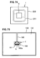
- FIG. 74 is a plan view of an electromagnetic coupling module according to a modification of a preferred embodiment, used in a radio IC device according to the present invention.
- FIG. 75 is a plan view of a radio IC device according to another preferred embodiment of the present invention.
- FIG. 1 shows portions of an electronic apparatus including a radio IC device according to a first preferred embodiment of the present invention.
- the electronic apparatus includes a printed wiring board 20 on which an electromagnetic coupling module 1 and other electronic components 26 , such as a chip resistor and a chip capacitor, for example, are mounted.
- the printed wiring board also includes a shielding electrode 27 therein.
- the electromagnetic coupling module 1 preferably includes a radio IC chip 5 processing a transmitted/received signal having a predetermined frequency and a feed circuit board 10 on which the radio IC chip 5 is disposed, as shown in FIG. 2 .
- a shielding case 28 of an apparatus also defines a radiation plate that functions as an antenna element, and is electrically connected to second wiring electrodes 21 a and 21 b (see FIGS. 2 and 4 ) magnetically coupled to the electromagnetic coupling module 1 on the printed wiring board 20 .
- the electromagnetic coupling module 1 and the radiation plate (shielding case 28 ) define the radio IC device.
- the radio IC chip 5 preferably includes a clock circuit, a logic circuit, a memory circuit and other circuit elements, and stores necessary information.
- input/output terminal electrodes 6 and packaging terminal electrodes 7 are disposed, as shown in FIG. 3 .
- the input/output terminal electrodes 6 are electrically connected to electrodes 12 a and 12 b (see FIGS. 7 and 8 ) disposed on the surface of the feed circuit board 10 preferably through metal bumps 8 , for example.
- the packaging terminal electrodes 7 are electrically connected to electrodes 12 c and 12 d through the metal bumps 8 .
- the material of the metal bumps 8 can preferably be Au, Ag, solder or other suitable material, for example.
- a protective film 9 is provided between the surface of the feed circuit board 10 and the rear surface of the radio IC chip 5 to improve the bonding strength between the feed circuit board 10 and the radio IC chip 5 and to protect the bumps 8 .
- the shielding case 28 is preferably made of a metal and arranged so as to cover the electromagnetic coupling module 1 and the electronic components 26 on the printed wiring board 20 .
- the shielding case functions as a radiation plate of the electromagnetic coupling module 1 , as will be described below.
- an electroconductive electrode film 28 ′ is preferably formed on the internal surface of the case 28 , as indicated by oblique lines shown in FIG. 4 , and the electrode film 28 ′ functions as the radiation plate.
- the feed circuit board 10 includes a feed circuit (including a resonance circuit having an inductance element and a matching circuit, not shown in FIG. 2 ), and is provided with external electrodes 19 a and 19 b from the rear surface to the sides. Also, the connection electrodes 12 a and 12 d (see FIGS. 7 and 8 ) are provided on the surface of the feed circuit board 10 .
- the external electrodes 19 a and 19 b are electromagnetically coupled to the resonance circuit included in the feed circuit board 10 and electrically connected to the second wiring electrodes 21 a and 21 b with an electroconductive adhesive 29 .
- the electrical connection may preferably be established by soldering, for example.
- the feed circuit board 10 includes a resonance circuit having a predetermined resonance frequency that transmits a signal having the predetermined frequency generated from the radio IC chip 5 to the shielding case 28 (or the electrode film 28 ′) through the external electrodes 19 a and 19 b and the wiring electrodes 21 a and 21 b , and supplies a signal having the predetermined frequency selected from the signals received by the shielding case 28 (or the electrode film 28 ′) to the radio IC chip 5 .
- the radio IC chip 5 operates according to the signal received by the shielding case (or the electrode film 28 ′), and an answer signal from the radio IC chip 5 is radiated from the shielding case 28 (or the electrode film 28 ′).
- the external electrodes 19 a and 19 b disposed on the surface of the feed circuit board 10 are electromagnetically coupled to the resonance circuit included in the feed circuit board 10 and electrically connected to the shielding case 28 which functions as an antenna.
- the electromagnetic coupling module 1 does not require a separate, relatively large antenna element, and accordingly the electromagnetic coupling module can be very small. Since the feed circuit board 10 has been miniaturized, the radio IC chip 5 can preferably be mounted on a miniaturized feed circuit board 10 by a conventionally used IC mounter or other suitable mounter, for example, and thus, the packaging cost can be reduced. All that is required to change the working frequency is to modify the design of the feed circuit, and the shielding case 28 may be used without being modified.
- the shielding case 28 is relatively large and can ensure desired radiation characteristics.
- the electroconductive adhesive 29 used to bond the external electrodes 19 a and 19 b with the second wiring electrodes 21 a and 21 b includes metal particles.
- Such an adhesive 29 exhibits a small difference in thermal expansion from the external electrodes 19 and 19 b and the wiring electrodes 21 a and 21 b when undergoing temperature changes, and accordingly, the bonding reliability is improved.
- the second wiring electrodes 21 a and 21 b may be provided within the printed wiring board 20 .
- the second wiring electrodes 21 a and 21 b are electrically connected to the electrodes on the surface of the wiring board 20 through a known via hole conductor.
- the printed wiring board 20 may preferably be a ceramic multilayer substrate or a resin substrate, for example.
- FIG. 5 shows essential portions of an electronic apparatus including a radio IC device according to a second preferred embodiment of the present invention.
- the electronic apparatus includes a plurality of printed wiring boards 31 and 32 covered with a case 33 .
- the printed wiring boards 31 and 32 are disposed on a substrate 30 .
- One printed wiring board 31 is provided with an electromagnetic coupling module 1 and other electronic components thereon, and the other printed wiring board 32 is provided with other electronic components thereon.
- the external electrodes 19 a and 19 b (see FIG. 2 ) of the electromagnetic coupling module 1 are electrically connected to second wiring electrodes 21 a and 21 b disposed on the printed wiring board 31 , as shown in FIG. 6 .
- the wiring electrodes 21 a and 21 b are connected to one end of a wiring cable 36 defining a first wiring electrode provided to a known wiring connector 35 .
- the other end of the wiring cable 36 is fixed to a securing member 37 disposed on the printed wiring board 32 and is electrically open.
- the wiring cable 36 between the wiring boards 31 and 32 functions as a radiation plate of the electromagnetic coupling module 1 .
- an RFID system is defined, and transmits and receives high-frequency signals to and from a reader/writer.
- the same effects are produced as in the first preferred embodiment.
- FIG. 7 shows a resonance circuit according to a first preferred embodiment, in which the feed circuit board 10 includes the resonance circuit.
- the feed circuit board 10 is preferably prepared by stacking dielectric ceramic sheets 11 A to 11 H, and pressing and firing the stack.
- the sheet 11 A is provided with connection electrodes 12 a and 12 b , electrodes 12 c and 12 d , and via hole conductors 13 a and 13 b .
- the sheet 11 B is provided with a capacitor electrode 18 a , conductor patterns 15 a and 15 b , and via hole conductors 13 c to 13 e .
- the sheet 11 C is provided with a capacitor electrode 18 b and via hole conductors 13 d to 13 f .
- the sheet 11 D is provided with conductor patterns 16 a and 16 b and via hole conductors 13 e , 13 f , 14 a , 14 b and 14 d .
- the sheet 11 E is provided with conductor patterns 16 a and 16 b and via hole conductors 13 e , 13 f , 14 a , 14 c and 14 e .
- the sheet 11 F is provided with a capacitor electrode 17 , conductor patterns 16 a and 16 b and via hole conductors 13 e , 13 f , 14 f and 14 g .
- the sheet 11 G is provided with conductor patterns 16 a and 16 b and via hole conductors 13 e , 13 f , 14 f and 14 g .
- the sheet 11 H is provided with conductor patterns 16 a and 16 b and a via hole conductor 13 f.
- a conductor pattern 16 a is preferably provided in a spiral arrangement, for example, continuing through the via hole conductors 14 c , 14 d and 14 g , thus defining an inductance element L 1
- a conductor pattern 16 b is preferably provided in a spiral arrangement, for example, continuing through the via hole conductors 14 b , 14 e and 14 f , thus defining an inductance element L 2
- a capacitance element C 1 is defined by capacitor electrodes 18 a and 18 b
- a capacitance element C 2 is defined by capacitor electrodes 18 b and 17 .
- One end of the inductance element L 1 is connected to the capacitor electrode 18 b through the via hole conductor 13 d , conductor pattern 15 a and the via hole conductor 13 c , and one end of the inductance element L 2 is connected to the capacitor electrode 17 through the via hole conductor 14 a .
- the other ends of the inductance elements L 1 and L 2 are brought together on the sheet 11 H and connected to the connection electrode 12 a through the via hole conductor 13 e , the conductor pattern 15 b and the via hole conductor 13 a .
- the capacitor electrode 18 a is electrically connected to the connection electrode 12 b through the via hole conductor 13 b.
- connection electrodes 12 a and 12 b are electrically connected to the input/output terminal electrodes 6 (see FIG. 3 ) of the radio IC chip 5 through the metal bumps 8 (see FIG. 2 ).
- the electrodes 12 c and 12 d are connected to the packing terminal electrodes 7 of the radio IC chip 5 .
- the external electrodes 19 a and 19 b are provided on the rear surface of the feed circuit board 10 preferably by applying a conductive paste, for example.
- the external electrode 19 a is coupled to the inductance elements L (L 1 and L 2 ) by a magnetic field, and the external electrode 19 b is connected to the capacitor electrode 18 b through the via hole conductor 13 f .
- the external electrodes 19 a and 19 b are electrically connected to the wiring electrodes 21 a and 21 b , as described above.
- the inductance elements L 1 and L 2 are arranged such that two conductor patterns 16 a and 16 b are disposed in parallel or substantially in parallel.
- the two conductor patterns 16 a and 16 b preferably have different line lengths from each other so as to have different resonance frequencies.
- the radio IC device can be used for a wide range of frequencies.
- the ceramic sheets 11 A to 11 H may be made of a magnetic ceramic material, and the feed circuit board 10 can be easily produced by a known process for forming a multilayer substrate, such as stacking sheets or printing into a thick film, for example.
- the sheets 11 A to 11 H may preferably be flexible sheets made of, for example, a dielectric material such as polyimide or liquid crystal polymer. Electrodes or conductors are formed on such flexible sheets by a thick film forming process, for example, and then the sheets are stacked one on top of another and thermally compressed into a multilayer composite. Thus, the inductance elements L 1 and L 2 and the capacitance elements C 1 and C 2 may be disposed within the circuit board.
- the inductance elements L 1 and L 2 and the capacitance elements C 1 and C 2 are disposed at different positions when viewed from above.
- the inductance elements L 1 and L 2 are coupled to the external electrode 19 a (wiring electrode 21 a ) by a magnetic field
- the capacitance element C 1 is coupled to the external electrode 19 b (wiring electrode 21 b ) by an electric field.
- the electromagnetic coupling module 1 including the radio IC chip 5 on the feed circuit board 10 receives high-frequency signals (for example, UHF frequencies) radiated from a reader/writer (not shown) with a shielding case 28 or a wiring cable 36 , so that the resonance circuit coupled to the external electrodes 19 a and 19 b through the wiring electrodes 21 a and 21 b by a magnetic field and an electric field resonates to supply only a received signal having a predetermined frequency to the radio IC chip 5 . A predetermined energy is extracted from the received signal.
- high-frequency signals for example, UHF frequencies
- the energy is used as a driving source to match the information stored in the radio IC chip 5 with a predetermined frequency by a resonance circuit, and to transmit the information to the shielding case 28 or the wiring cable 36 through the external electrodes 19 a and 19 b and the wiring electrodes 21 a and 21 b , and further transmit or transfer the information to the reader/writer from the case 28 or the cable 36 .
- the resonance frequency characteristics of the feed circuit board 10 depend on the resonance circuit including the inductance elements L 1 and L 2 and the capacitance elements C 1 and C 2 .
- the resonance frequency of the signal radiated from the shielding case 28 or the wiring cable 36 substantially depends on the self resonant frequency of the resonance circuit. It is accordingly not necessary to redesign the resonance circuit even if the shielding case 28 or the wiring cable 36 is changed in shape or material. Thus, the resonance circuit can be applied to various electronic apparatuses.
- the resonance circuit preferably also defines a matching circuit to match the impedances between the radio IC chip 5 and the radiation plate (shielding case 28 or wiring cable 36 ).
- the feed circuit board 10 may preferably include a matching circuit provided in addition to the resonance circuit including the inductance elements and the capacitance elements (in this sense, the resonance circuit may be referred to as matching circuit).
- the design for a resonance circuit also defining a matching circuit tends to be complicated. A structure in which a matching circuit is provided separately from the resonance circuit enables the resonance circuit and the matching circuit to be independently designed.
- the resonance circuit may be replaced with a matching circuit.
- the resonance circuit may be designed in view of the shape and size of the radiation plate, or the shielding case 28 or the wiring cable 36 . Although this requires that the feed circuit board 10 be precisely mounted at a correct position, the radiation characteristics of the resulting radio IC device can be improved.
- FIG. 8 shows a resonance circuit according to a second preferred embodiment, in which the resonance circuit is disposed on a feed circuit board 40 .
- This feed circuit board 40 is preferably made of a flexible PET film, for example, and on which a spiral conductor pattern 42 defining inductance elements L and a capacitor electrode 43 defining a capacitance element C are disposed.
- Electrodes 12 a and 12 b extending from the conductor pattern 42 and the capacitor electrode 43 are electrically connected to the terminal electrodes 6 of the radio IC chip 5 .
- Electrodes 12 c and 12 d provided on the circuit board define terminal ground electrodes and are electrically connected to the terminal electrodes 7 of the radio IC chip 5 .
- the feed circuit board 40 is substantially the same as that of the first preferred embodiment in that the inductance elements L and the capacitance element C define a resonance circuit and are coupled to the respectively opposing second wiring electrodes 21 a and 21 b by a magnetic field and an electric field to transmit and receive a high-frequency signal having a predetermined frequency.
- the feed circuit board 40 made of a flexible film produces a thin electromagnetic coupling module 1 .
- the inductances of the inductance elements L can be varied by varying the line width and/or the line pitch of the conductor pattern 42 , and thus the resonance frequency can be precisely adjusted.
- the conductor pattern 42 defining the inductance elements L preferably includes two spiral lines that are connected to each other at the approximate center of the spirals.
- the two lines of the conductor pattern 42 have respective inductances L 1 and L 2 and their resonance frequencies can be set to different values.
- the resulting radio IC device can be used in a wide range of frequencies as that of the first preferred embodiment.
- second wiring electrodes 22 a and 22 b are preferably configured in a meandering arrangement on the printed wiring board 20 of an electronic apparatus.
- the electromagnetic coupling module 1 is mounted on one end of each of the wiring electrodes 22 a and 22 b , as shown in FIG. 9 .
- a metal case 50 of a battery or liquid crystal panel is disposed close to the electrode 22 b on the printed wiring board 20 .
- the electromagnetic coupling module 1 is coupled to the wiring electrodes 22 a and 22 b in substantially the same manner as in the first and second preferred embodiments.
- the second wiring electrodes 22 a and 22 b function as the radiation plate, and the metal case 50 via the wiring electrode 22 b is coupled to the wiring electrode 22 b to function as the radiation palate.
- the wiring electrodes 22 a and 22 b themselves may function as the radiation plate, and, in addition, the metal case 50 is also used as the radiation plate. Consequently, the radiation characteristics and the antenna gain are improved.
- the radio IC device of the third preferred embodiment can function without the metal case 50 . By matching the resonance frequency of the metal case 50 to the working frequency of the radio IC device, the antenna gain can be further improved.
- the radio IC device has substantially the same structure as that of the third preferred embodiment, except that a portion of the metal case 50 used in the third preferred embodiment is disposed on the wiring electrode 22 b , as shown in FIG. 10 .
- the fourth preferred embodiment produces substantially the same effects as the third preferred embodiment. Since the metal case 50 overlaps the wiring electrode 22 b , particularly, the degree of their coupling is increased.
- the wiring electrode 22 a is electrically connected to a ground electrode 23 disposed on the printed wiring board 20 , and the other wiring electrode 22 b is disposed close to the metal case 50 , as shown in FIG. 11 .
- the ground electrode 23 may be included in the printed wiring board 20 .
- the wiring electrode 22 a may be connected to the ground electrode 23 through a via-hole conductor, or may be configured to have a meandering arrangement as shown in FIG. 9 and overlap the ground electrode 23 .
- the wiring electrode 22 b and the metal case 50 function as a radiation plate, and, in addition, the ground electrode 23 connected to the wiring electrode 22 a also function as a radiation plate. Since the ground electrode 23 has a large area, the radiation characteristics and the antenna gain are improved.
- the radio IC device has substantially the same structure as that of the fifth preferred embodiment except that a portion of the metal case 50 used in the fifth preferred embodiment is disposed on the wiring electrode 22 b , as shown in FIG. 12 .
- the sixth preferred embodiment produces substantially the same effects as the fifth preferred embodiment. Since the metal case 50 overlaps the wiring electrode 22 b , particularly the degree of their coupling is increased.
- a loop electrode 24 defining the second wiring electrode is disposed on the printed wiring board 20 , and the electromagnetic coupling module 1 is disposed on both ends of the line of the loop electrode 24 , as shown in FIG. 13 .
- the metal case 50 is disposed close to the loop electrode 24 on the printed wiring board 20 .
- the electromagnetic coupling module 1 is coupled to the loop electrodes 24 in substantially the same manner as in the first and the second preferred embodiment.
- the loop electrode 24 functions as a radiation plate, and the metal case coupled to the loop electrode 24 also functions as a radiation plate.
- the loop electrode 24 can match the impedances between the radio IC chip 5 and the radiation plate, and thus improves the signal transmission efficiency between the radio IC chip 5 and the radiation plate without requiring an additional matching portion.
- the metal case 50 used in the sixth preferred embodiment (see FIG. 12 ) is disposed on the rear surface of the printed wiring board 20 , as shown in FIG. 14 .
- a portion of the metal case 50 is coupled to the wiring electrode 22 b with the printed wiring board 20 therebetween.
- the other structure is substantially the same as in the sixth preferred embodiment.
- the eighth preferred embodiment produces substantially the same effects as the sixth preferred embodiment. Since the metal case 50 is disposed on the rear surface of the printed wiring board 20 , the ground electrode 23 can be provided with a large area.
- another metal case 51 is included close to the wiring electrode 22 a on the surface of the printed wiring board 20 of the third preferred embodiment (see FIG. 9 ), as shown in FIG. 15 .
- the metal case 51 is coupled to the wiring electrode 22 a to function as a radiation plate, and, thus, the antenna gain is further improved.
- the metal case 51 used in the ninth preferred embodiment is disposed on the rear surface of the printed wiring board 20 , as shown in FIG. 16 .
- the metal case is coupled to the wiring electrode 22 a with the printed wiring board 20 therebetween.
- the printed wiring board 20 is enclosed by an upper and a lower metal case 52 and 53 , as shown in FIGS. 17 and 18 , and the metal cases 52 and 53 function as radiation plates.
- Wiring electrodes 22 a and 22 b are provided on the printed wiring board 20 and coupled to the electromagnetic coupling module 1 .
- the wiring electrode 22 a is disposed on the rear side and connected to the front side through a via hole conductor.
- the wiring electrode 22 b is disposed on the front side.
- the metal case 52 has a coupling conductor 52 a to enable the metal case 52 to couple efficiently to the wiring electrode 22 b
- the metal case 53 has a coupling conductor 53 a to enable the metal case 53 to couple efficiently to the wiring electrode 22 a.
- the wiring electrodes 22 a and 22 b function as radiation plates, and the metal cases 52 and 53 coupled to the respective wiring electrodes 22 a and 22 b also function as the radiation plates.
- the radiation characteristics and the antenna gain are improved.
- a portion of the metal case 50 is disposed on the ground electrode 23 connected to the wiring electrode 22 a as in the fifth preferred embodiment (see FIG. 11 ), as shown in FIG. 20 .
- the ground electrode 23 and the metal case 50 are coupled to each other to function as a radiation plate.
- the area of the loop electrode 25 provided as the second wiring electrode is increased as shown in FIG. 21 so that the loop electrode 25 can be used as a ground electrode 23 or a power supply electrode.
- the metal case 50 is disposed on a portion of the loop electrode 25 .
- the loop electrode 25 and the metal case 50 function as a radiation plate.
- the loop electrode 25 provided as the second wiring electrode and the ground electrode 23 are integrated to function as a radiation plate, and a metal case 54 electrically connected to the ground electrode 23 is disposed on the printed wiring board 20 so as to cover the radiation plate, as shown in FIG. 22 .
- the metal case 54 has a notch 55 in a region corresponding to the loop electrode 25 when viewed from above. Since a magnetic field is generated around the loop electrode 25 , the magnetic field is radiated out of the metal case 54 through the notch 55 over the loop electrode 25 . Thus, the radiation characteristics are improved.
- the metal case 54 may be disposed so as to cover at least one of other electronic components (not shown).
- a ground electrode 101 including an opening 102 is disposed on a printed wiring board 100 , and a pair of loop electrodes 103 functioning as inductance elements are provided in the opening 102 , as shown in FIG. 23 .
- the electromagnetic coupling module 1 (or radio IC chip 5 alone) is coupled to the end of each loop electrode 103 .
- the printed wiring board 100 includes switching modules 105 , ICs 106 , and other elements 107 , such as chip resistors and chip capacitors thereon.
- the printed wiring board 100 is covered with a shielding case 109 .
- a USB connector 110 is connected to the printed wiring board 100 .
- the metal portion of the connector 110 is electrically connected to the ground electrode 101 and functions as a radiation plate of the electromagnetic coupling module 1 .
- the ground electrode 101 includes a slit 104 in the vicinity of the connector 110 , so that electromagnetic waves through the connector 110 can efficiently propagate to the loop electrodes 103 .
- FIG. 24 shows a state before the shielding case 109 and the connector 110 are disposed on the printed wiring board 100 .
- the ground electrode 101 functions as a radiation plate.
- the structure of the fifteenth preferred embodiment can function as a radio IC device from a stage shown in FIG. 24 to the final stage shown in FIG. 23 of the manufacturing process.
- the shielding wire 111 a of a coaxial cable (power supply cable) 111 is electrically connected to the ground electrode 101 disposed on the printed wiring board 100 , as shown in FIG. 25 .
- the other structure is substantially the same as in the fifteenth preferred embodiment.
- the shielding wire 111 a of the coaxial cable 111 electrically connected to the ground electrode 101 functions as a radiation plate of the electromagnetic coupling module 1 . Since the shielding wire 111 a is relatively long, communication can be performed even with weak electromagnetic waves.
- a slot case 112 of a USB card is electrically connected to the ground electrode 101 disposed on the printed wiring board 100 , as shown in FIG. 26 .
- the other structure is substantially the same as in the fifteenth preferred embodiment.
- the slot case 112 is a metal component, and is electrically continued to the ground electrode 101 to function as a radiation plate of the electromagnetic coupling module 1 .
- the metal case of a battery 113 is electrically connected to the ground electrode 101 disposed on the printed wiring board 100 , as shown in FIG. 27 .
- the other structure is substantially the same as in the fifteenth preferred embodiment.
- the metal case of the battery 113 is electrically connected to the ground electrode 101 to function as the radiation plate of the electromagnetic coupling module 1 .
- the shielding case 109 of the fifteenth preferred embodiment shown in FIG. 23 is electrically connected to the ground electrode 101 through a conductor portion 109 a , as shown in FIG. 28 .
- the other structure is substantially the same as in the fifteenth preferred embodiment.
- the shielding case 109 as well as the metal portion of the connector 110 functions as a radiation plate.
- the ground electrode 101 includes a slit 104 in the vicinity of the conductor portion 109 a , so that electromagnetic waves through the shielding case 109 can efficiently propagate to the loop electrode 103 .
- the shielding case 109 of the sixteenth preferred embodiment shown in FIG. 25 is electrically connected to the ground electrode 101 through a conductor portion 109 a , as shown in FIG. 29 .
- the other structure is substantially the same as in the sixteenth preferred embodiment.
- the shielding case 109 as well as the shielding wire 111 a of the coaxial cable 111 functions as a radiation plate.
- the ground electrode 101 includes a slit 104 in the vicinity of the conductor portion 109 a , so that electromagnetic waves through the shielding case 109 can efficiently propagate to the loop electrode 103 .
- a ground electrode 121 disposed on a printed wiring board 120 includes a slit opening 121 a , as shown in FIG. 30 .
- a wiring electrode (hereinafter referred to as power line 122 ) is provided in the slit opening 121 a .
- a power supply cable 128 is connected to the ground electrode 121
- another power supply cable 129 is connected to the power line 122 .
- the electromagnetic coupling module 1 is bonded on the power line 122 .
- the printed wiring board 120 is covered with a shielding case 127 and the power supply cables 128 and 129 extend a relatively long distance out of the shielding case 127 .
- the power line 122 is provided with a capacitor 125 to reject high-frequency noises, a voltage regulator 126 and other interference to stabilize the voltage.
- the electromagnetic coupling module 1 includes a feed circuit board 130 including a coil (inductance element) 131 , a radio IC chip 5 on the feed circuit board 130 , and a resin protecting member 141 covering the feed circuit board 130 and the radio IC chip 5 , as shown in FIG. 32 .
- the coil 131 is arranged such that the coil axis extends parallel or substantially parallel to the power line 122 , and each end of which is electrically connected to the radio IC chip 5 .
- the power supply cable 129 receives magnetic waves from a reader/writer (not shown)
- the power line 122 generates a current, as shown in FIG. 31 .
- the current flows to the ground electrode 121 through the capacitor 125 to generate a magnetic field ⁇ at the power line 122 .
- the magnetic field ⁇ is coupled to the coil 131 of the feed circuit board 130 , thus operating the radio IC chip 5 .
- the power supply cable 129 functions as a radiation plate. Also, the power line 122 functions as a radiation plate in the course of the manufacturing process in which the shielding case 127 or the power supply cable 129 is not provided.
- the power supply cable 129 may be directly connected to the reader/writer.
- the feed circuit board 130 of the electromagnetic coupling module 1 is provided with a matching circuit/resonance circuit 132 in addition to the coil 131 , as shown in FIG. 33 .
- the other structure is substantially the same as in the twenty first preferred embodiment.
- the twenty second preferred embodiment produces substantially the same effects as the twenty first preferred embodiment.
- the circuit 132 is a matching circuit
- the matching with the coil 131 can be provided, so that the radio IC chip 5 can be operated even at a low power.
- the radio IC chip can be frequency-selective, and accordingly, the variation in frequency can be reduced.
- the radio IC chip can work in a wide range of frequencies.
- the feed circuit board 130 of the electromagnetic coupling module 1 is provided with a pair of external terminal electrodes 133 on the rear surface thereof, as shown in FIG. 34 .
- the other structure is substantially the same as in the twenty first preferred embodiment.
- the twenty third preferred embodiment produces substantially the same effects as the twenty first preferred embodiment.
- the external terminal electrodes 133 provided on the rear surface of the feed circuit board 130 allow the electromagnetic coupling module 1 to be joined to the power line 122 with solder, for example.
- the electromagnetic coupling module 1 can be mounted simultaneously with other surface mount components.
- only a single external terminal electrode 133 may be formed at substantially the center of the rear surface of the feed circuit board 130 .
- the feed circuit board 130 of the electromagnetic coupling module 1 is provided with a pair of external terminal electrodes 133 on the rear surface thereof, as shown in FIG. 35 .
- a conductor 134 is disposed within the feed circuit board 130 on the rear surface side, and the power line 122 is cut under the conductor 134 .
- the other structure is substantially the same as in the twenty first and the twenty third preferred embodiment.
- the twenty fourth preferred embodiment produces substantially the same effects as the twenty first and the twenty third preferred embodiment. Since the current running in the power line 122 is conducted to flow near the coil 131 by the conductor 134 , the degree of coupling is improved, and accordingly, the radio IC chip can operate at a low power. In addition, the variation in coupling degree is reduced.
- an auxiliary substrate 140 is provided on which an electromagnetic coupling module 1 is mounted, as shown in FIG. 36 .
- a coupling electrode 141 having an opening 142 is provided on the auxiliary substrate 140 , and a pair of loop electrodes 143 functioning as inductance elements is provided in the opening 142 .
- the electromagnetic coupling module 1 (or radio IC chip 5 alone) is coupled to the end of each loop electrode 143 .
- the other structure is substantially the same as in the twenty first preferred embodiment.
- the electromagnetic coupling module 1 is coupled to the loop electrodes 143 , and in addition, the coupling electrode 141 is coupled to the power line 122 .
- the use of the auxiliary substrate 140 enables the use of a large coupling electrode 141 or the increase of the coil 131 in the feed circuit board 130 .
- the degree of coupling to the power line 122 can be increased.
- the coupling electrode 141 on the auxiliary substrate 140 can function as the radiation plate by itself, and can be disposed anywhere on the printed wiring board 120 .
- a power line 122 on which the electromagnetic coupling module 1 is mounted is arranged so as to extend a relatively long distance in the lateral direction along an edge of the printed wiring board 120 , as shown in FIG. 37 .
- the other structure is substantially the same as in the twenty first preferred embodiment (see FIG. 30 ).
- the twenty sixth preferred embodiment produces substantially the same effects as the twenty first preferred embodiment.
- the lengthened power line 122 functions as the radiation plate and allows the radio IC device to function before the shielding case 127 or the power supply cable 129 is provided.
- the power line 122 shown in FIG. 37 is branched so as to extend a relatively long distance in the lateral direction along an edge of the printed wiring board 120 , as shown in FIG. 38 .
- the other structure is substantially the same as in the twenty first and the twenty sixth preferred embodiment. Since the power line 122 functioning as a radiation plate of the twenty seventh preferred embodiment is longer than that of the twenty sixth preferred embodiment, electromagnetic waves can be more efficiently transmitted and received, and the operation can be performed at a low power.
- the power line 122 has a length that enables it to resonate.
- the extensions of the power line 122 shown in FIG. 38 are configured in a meandering arrangement, as shown in FIG. 39 .
- the other structure is substantially the same as in the twenty first preferred embodiment.
- the power line 122 functioning as a radiation plate is relatively large, and accordingly, electromagnetic waves can be transmitted and received more efficiently.
- the ground electrode 121 disposed on the printed wiring board 120 has a relatively large opening 121 b in which a plurality of line electrodes 145 are arranged in parallel or substantially in parallel with each other.
- the line electrodes 145 are connected to signal lines 146 , such as for a USB, and one of which is coupled to the electromagnetic coupling module 1 , as shown in FIG. 40 .
- a regulator 126 is disposed between the line electrodes 145 and the ground electrode 121 .
- the signal lines 146 functions as a radiation plate, and substantially the same effects are produced as in the twenty first preferred embodiment and other preferred embodiments.
- the radio IC device can function even though it is driven by a battery and does not have a power supply cable.
- the electrode 121 disposed on the printed wiring board 120 includes a slit opening 121 a , as shown in FIG. 41 .
- An antenna line 151 is disposed in the slit opening 121 a , and an antenna wire 152 is connected to the antenna line 151 .
- the electromagnetic coupling module 1 is coupled to the antenna line 151 .
- the regulator 126 is disposed between the antenna line 151 and the ground electrode 121 .
- the antenna wire 152 functions as a radiation plate, and substantially the same effects are produced as in the twenty first preferred embodiment and other preferred embodiments.
- the electromagnetic coupling module 1 is provided with a resonance circuit or a matching circuit so that energy is transmitted to the radio IC chip 5 only at a frequency at which the IC chip 5 operates as an RFID, thus preventing interference with the operation of the antenna.
- the antenna wire 152 intended to receive electromagnetic waves is efficiently used as a radiation plate. Accordingly, the operation can be performed at a low power.
- an anti-ESD device such as a varistor 153 , for example, is disposed between the power line 122 and the ground electrode 121 , and the electromagnetic coupling module 1 is disposed downstream from the varistor 153 , as shown in FIG. 42 .
- the other structure is substantially the same as in the twenty first preferred embodiment (see FIG. 30 ).
- the thirty first preferred embodiment produces substantially the same effects as the twenty first preferred embodiment.
- the presence of the varistor 153 improves the electrostatic surge resistance.
- the ground electrode 121 disposed on the printed wiring board 120 includes a slit opening 121 a , as shown in FIG. 44 .
- a power line 122 is disposed in the slit opening 121 a .
- a power supply cable 128 is connected to the ground electrode 121
- another power supply cable 129 is connected to the power line 122 .
- an electromagnetic coupling module 1 is bonded across the region between the power line 122 and the ground electrode 121 .
- the printed wiring board 120 is covered with a shielding case 127 and the power supply cables 128 and 129 extend long out of the shielding case 127 .
- the power line 122 is provided with a capacitor 125 for rejecting high-frequency noises, a voltage regulator 126 and the like to stabilize the voltage.
- the electromagnetic coupling module 1 includes the radio IC chip 5 and a feed circuit board 160 , as shown in FIG. 45 .
- the feed circuit board 160 includes inductance elements L 11 and L 12 magnetically coupled to each other, and a resonance circuit having a predetermined resonance frequency with capacitors defined by an internal electrode 161 and a ground electrode 121 and by an internal electrode 162 and a power line 122 .
- the radio IC chip 5 is electrically connected to the resonance circuit with solder bumps.
- reference numeral 156 designates an adhesive
- reference numeral 166 designates a protective layer for the solder bumps.
- the power line 122 when the power supply cable 129 receives magnetic waves from a reader/writer (not shown), the power line 122 generates a current.
- the power line 122 and the ground electrode 121 have a potential difference therebetween, because of the presence of an inductance component (in a coil form) as shown in FIG. 44 in view of high frequency.
- the occurrence of the potential difference enables the internal electrodes 161 and 162 of the feed circuit board 160 to be electromagnetically coupled to the ground electrode 121 and the power line 122 , so that a signal operates the radio IC chip 5 through the resonance circuit.
- the power supply cable 129 functions as a radiation plate, and substantially the same effects are produced as in the twenty first preferred embodiment (see FIG. 30 ). Since the feed circuit board 160 includes the resonance circuit including the inductance elements L 11 and L 12 and the capacitor, the feed circuit board functions of matching with the radio IC chip 5 and a function of selecting frequency. Thus, signals can be transmitted in a wide range of frequencies.
- the electromagnetic coupling module 1 may be replaced with only a radio IC chip 5 .
- the resonance circuit provided in the feed circuit board 160 of the electromagnetic coupling module 1 is defined by inductance elements L 11 , L 12 and L 13 coupled to each other, as shown in FIG. 46 .
- the other structure is substantially the same as in the thirty third preferred embodiment, and substantially the same effects are produced as in the thirty third preferred embodiment.
- the electromagnetic coupling module 1 can be mounted without considering the directivity.
- external terminal electrodes 163 and 164 that oppose the internal electrodes 161 and 162 are provided on the rear surface of the feed circuit board 160 , as shown in FIG. 47 .
- the other structure is substantially the same as in the thirty fourth preferred embodiment, and substantially the same effects are produced as in the thirty fourth preferred embodiment.
- the electromagnetic coupling module 1 can be bonded on the printed wiring board 120 with solder, for example, and thus, can be mounted simultaneously with other surface mount components.
- a power line 122 on which the electromagnetic coupling module 1 is mounted is provided so as to extend a relatively long distance in the lateral direction along an edge of the printed wiring board 120 , as shown in FIG. 48 .
- the other structure is substantially the same as in the thirty third preferred embodiment (see FIG. 44 ).
- the thirty sixth preferred embodiment produces substantially the same effects as the thirty third preferred embodiment.
- the lengthened power line 122 can more effectively function as the radiation plate and enables the radio IC device to function before the shielding case 127 or the power supply cable 129 is provided.
- the radio IC device according to a thirty seventh preferred embodiment, the extension of the power line 122 shown in FIG. 48 is configured in a meandering arrangement, as shown in FIG. 49 .
- the other structure is substantially the same as in the thirty third preferred embodiment.
- the power line 122 functioning as a radiation plate is relatively large, and accordingly, electromagnetic waves can be transmitted and received more efficiently.
- the power line 122 shown in FIG. 48 is branched so as to extend a relatively long distance in the lateral direction along an edge of the printed wiring board 120 , as shown in FIG. 50 .
- the other structure is substantially the same as in the thirty third and the thirty sixth preferred embodiment. Since the power line 122 functioning as a radiation plate of the thirty eighth preferred embodiment is longer than that of the thirty sixth preferred embodiment, electromagnetic waves can be more efficiently transmitted and received, and the operation can be performed at a low power.
- the power line 122 has a length which enables it to resonate.
- the extensions to both sides of the power line 122 are configured in a meandering arrangement, as shown in FIG. 51 .
- the other structure is substantially the same as in the thirty third preferred embodiment.
- the power line 122 functioning as a radiation plate is relatively large, and accordingly, electromagnetic waves can be transmitted and received more efficiently.
- a portion of the power line 122 is disposed under the printed wiring board 120 , as shown in FIG. 52 , and the electromagnetic coupling module 1 is mounted across the region between the power line 122 exposed at the surface and the ground electrode 121 .
- the power supply cable 129 is connected to an end 122 a of the power line exposed at the surface.
- the other structure is substantially the same as in the thirty third preferred embodiment, and substantially the same effects are produced as in the thirty third preferred embodiment.
- the power line 122 is partially disposed under the printed wiring board 120 , the flexibility of wiring on the surface is improved.
- the power line 122 is bent in a substantial C shape and both ends of the electromagnetic coupling module 1 are connected to the bent portions, as shown in FIG. 53 .
- the other structure is substantially the same as in the thirty third preferred embodiment, and substantially the same effects are produced as in the thirty third preferred embodiment.
- the electromagnetic coupling module 1 is mounted across the power line 122 from one end of the ground electrode 121 to the opposing end, as shown in FIG. 54 .
- the other structure is substantially the same as in the thirty third preferred embodiment, and the electromagnetic coupling module 1 is operated by a difference in potential produced on the ground electrode 121 .
- a portion 121 c of the ground electrode 121 coupled to the feed circuit of the electromagnetic coupling module 1 is formed in a loop, as shown in FIG. 56 .
- the other structure is substantially the same as in the thirty third and the forty second preferred embodiment, and substantially the same effects are produced as in the thirty third and the forty second preferred embodiments.
- the ground electrode 121 disposed on the printed wiring board 120 has a relatively large opening 121 b in which a plurality of line electrodes 145 are provided in parallel with each other.
- the line electrodes 145 are connected to signal lines 146 , such as for a USB, and the electromagnetic coupling module 1 is disposed across the region between the ground electrode 121 and one of the line electrodes 145 to be coupled to that one line electrode, as shown in FIG. 57 .
- a regulator 126 is disposed between the line electrodes 145 and the ground electrode 121 .
- the signal lines 146 function as a radiation plate using the difference in potential between the line electrode 145 and the ground electrode 121 , and substantially the same effects are produced as in the thirty third and the twenty ninth preferred embodiment.
- the ground electrode 121 disposed on the printed wiring board 120 includes a slit opening 121 a , as shown in FIG. 59 .
- An antenna line 151 is disposed in the slit opening 121 a
- an antenna wire 152 is connected to the antenna line 151 .
- the electromagnetic coupling module 1 is coupled so as to be disposed across a region between the antenna line 151 and the ground electrode 121 .
- the regulator 126 is disposed between the antenna line 151 and the ground electrode 121 .
- the antenna wire 152 functions as the radiation plate, and substantially the same effects are produced as in the thirty third and the thirtieth preferred embodiment.
- an auxiliary substrate 170 is provided on which the electromagnetic coupling module 1 is mounted, as shown in FIG. 60 .
- a coupling electrode 171 is provided on the auxiliary substrate 170 , and a pair of loop electrodes 173 functioning as inductance elements is provided for the coupling electrode 171 .
- the electromagnetic coupling module 1 (or radio IC chip 5 alone) is coupled to each end of the loop electrodes 173 .
- the ends of the coupling electrode 171 are connected to the power line 122 and the ground electrode 121 with solder 175 .
- the other structure is substantially the same as in the thirty third preferred embodiment.
- the electromagnetic coupling module 1 is coupled to the loop electrodes 173 , and in addition, the coupling electrode 171 is disposed across the region between the power line 122 and the ground electrode 121 so as to be coupled to the power line 122 and the ground electrode 121 .
- the use of the auxiliary substrate 170 enables even a small electromagnetic coupling module 1 to be disposed across the region between the power line 122 and the ground electrode 121 .
- an inductance element or other suitable element may be provided on the auxiliary substrate 170 in order to reduce the size of the feed circuit board 160 .
- the coupling electrode 171 on the auxiliary substrate 170 functions as a radiation plate by itself.
- an anti-ESD device such as a varistor 153 , for example, is disposed between the power line 122 and the ground electrode 121 , and an electromagnetic coupling module 1 is disposed downstream from the varistor 153 , as shown in FIG. 61 .
- the other structure is substantially the same as in the thirty third preferred embodiment (see FIG. 44 ).
- the forty eighth preferred embodiment produces substantially the same effects as the thirty third and the thirty first preferred embodiment.
- a ground electrode 181 disposed on a printed wiring board 180 includes an opening 182 to define a loop electrode 183 , and the electromagnetic coupling module 1 is mounted on the loop electrode 183 , as shown in FIG. 62 .
- the electromagnetic coupling module 1 includes the radio IC chip 5 and a feed circuit board 190 .
- the feed circuit board 190 includes a coil (inductance element) 191 , as shown in FIG. 64 .
- the coil 191 is arranged such that the coil axis extends parallel or substantially parallel to the loop electrode 183 , and each end of the coil 191 is electrically connected to the radio IC chip 5 .
- the loop electrode 183 when the ground electrode 181 receives magnetic waves from a reader/writer (not shown), the loop electrode 183 generates a current.
- the magnetic field ⁇ generated by the current is coupled to the coil 191 of the feed circuit board 190 , thus operating the radio IC chip 5 .
- the electromagnetic coupling module 1 is arranged such that a magnetic field ⁇ intersects only one side of the coil 191 .
- a matching circuit/resonance circuit 192 may be provided within the feed circuit board 190 , as shown on FIG. 65 .
- the elements 105 , 106 and 107 disposed on the printed wiring board 180 are substantially the same as in the fifteenth preferred embodiment (see FIG. 23 ).
- the loop electrode 183 provided on the ground electrode 181 is bent in a substantial C shape, and the electromagnetic coupling module 1 is mounted such that the coil 191 is disposed along the loop electrode 183 , as shown in FIG. 66 .
- the other structure is substantially the same as in the forty ninth preferred embodiment.
- the electromagnetic coupling module 1 is disposed in a reverse orientation to that in the forty ninth preferred embodiment (see FIG. 62 ) on the printed wiring board 180 , as shown in FIG. 67 .
- the other structure is substantially the same as in the forty ninth preferred embodiment, and substantially the same effects are produced as in the forty ninth preferred embodiment.
- it is an advantage that the electromagnetic coupling module 1 does not significantly protrude from the edge of the printed wiring board 180 .
- the feed circuit board 190 includes a coil 191 arranged such that the coil axis extends perpendicular or substantially perpendicular to the loop electrode 183 , as shown in FIG. 68 .
- the fifty second preferred embodiment produces substantially the same effects as the forty ninth preferred embodiment.
- the coil 191 is arranged such that the coil axis extends in the direction in which the sheets of the feed circuit board 190 are stacked, and this facilitates the formation of the coil 191 .
- the electromagnetic coupling module 1 is mounted at an edge of the ground electrode 181 without providing a loop electrode 183 on the ground electrode 181 , as shown in FIG. 69 .
- the other structure is substantially the same as in the forty ninth preferred embodiment, and substantially the same effects are produced as in the forty ninth preferred embodiment.
- the electromagnetic coupling module 1 is operated by being coupled with a magnetic field generated by the current flowing in the edge of the ground electrode 181 .
- a notch 184 is provided in the printed wiring board 180 , and the ground electrode 181 includes a loop electrode 183 at the edge around the notch 184 , as shown in FIG. 70 .
- the other structure is substantially the same as in the forty ninth preferred embodiment, and substantially the same effects are produced as in the forty ninth preferred embodiment.
- the electromagnetic coupling module 1 is arranged in a corner of the ground electrode 181 as shown in FIG. 71 , unlike the fifty third preferred embodiment in which the electromagnetic coupling module 1 is disposed substantially at the center of an edge of the ground electrode 181 .
- the other structure is substantially the same as in the forty ninth and the fifty third preferred embodiment, and substantially the same effects are produced as in the forty ninth and fifty third preferred embodiment.
- the electromagnetic coupling module 1 can be disposed anywhere on the edge of the ground electrode 181 .
- a notch may be provided in the corner of the printed wiring board 180 on which the electromagnetic coupling module 1 is disposed, as disclosed in the fifty fourth preferred embodiment, and the ground electrode 181 has a loop electrode at the edge around the notch.
- a coil 195 in a feed circuit board 190 has a substantial figure 8 shape, as shown in FIG. 72 , and the other structure is substantially the same as in the forty ninth preferred embodiment (see FIG. 62 ).
- the electromagnetic coupling module 1 is arranged on the printed wiring board 180 such that the magnetic flux ⁇ generated from the loop electrode 183 can pass through the loops of the coil 195 functioning as inductance elements, as shown in FIG. 73 .
- the ground electrode 181 functioning as a radiation plate and the electromagnetic coupling module 1 can be highly coupled.
- the electromagnetic coupling module 1 may preferably include a square feed circuit board 200 , as shown in FIG. 74 .
- the coil 201 functioning as an inductance element also has a square shape. This electromagnetic coupling module 1 can be applied to any preferred embodiment of the present invention.
- a slit 185 is provided in the ground electrode 181 disposed on the printed wiring board 180 , extending from the edge to the approximate center.
- the slit 185 has an opening 185 a at the end thereof, and the electromagnetic coupling module 1 is disposed over the opening 185 a , as shown in FIG. 75 .
- the coil 191 provided on the feed circuit board 190 and the opening 185 a have substantially the same shape in plan view.
- the surrounding of the opening 185 a functions as a loop electrode to be magnetically coupled to the coil 191 .
- the presence of the slit 185 improves the concentration of the current produced by the electromagnetic waves received by the ground electrode 181 around the opening 185 a to generate a strong magnetic field, thus improving the degree of coupling.
- the feed circuit board may preferably have a resonance circuit through which the radio IC is operated by the signal received by the radiation plate, and through which the answer signal from the radio IC is radiated from the radiation plate to the outside.
- the feed circuit board may include a matching circuit.
- the inductance element may preferably be defined by a spiral electrode, for example, and the spiral electrode may be coupled with a magnetic field generated at the wiring electrode on the wiring board.
- the wiring electrode and the ground electrode on the wiring board may be isolated from each other, and the feed circuit board may be disposed across a region between the wiring electrode and the ground electrode. If the case is a metal, the case may function as a radiation plate by itself. If the case is non-conductive, an electroconductive electrode film may be formed on the case and the electrode film is used as the radiation plate.
- the printed wiring board may include a second wiring electrode arranged to couple the feed circuit and the radiation plate, and a case may be arranged so as to cover all the electronic components and high frequency device mounted on the printed wiring board.
- the second wiring electrode may function as a portion of the radiation plate. In this instance, the radiation characteristics can be improved, and the directivity can be changed depending on the arrangement of the second wiring electrode. At least a portion of the electronic components may function as a portion of a radiation plate to improve the radiation characteristics.
- the printed wiring board may include a ground electrode, and a second wiring electrode may be electrically connected to the ground electrode.
- a ground electrode having a large area as a radiation plate, the radiation characteristics can further be improved.
- the second wiring electrode may be provided on the surface of or within the printed wiring board.
- the printed wiring board may be made of a resin or a ceramic, for example.
- An external electrode coupled to the feed circuit may be formed on the surface of the feed circuit board.
- the radio IC may be rewritable as well as storing information of the commodity on which the radio IC device is attached, and may have other functions in addition to the function for an RFID system.
- radio IC device is not limited to the above-described preferred embodiments, and various modifications may be made without departing from the scope of the present invention.
- radio IC chip can be mounted on the feed circuit board by any method other than using a metal bump.
- the radio IC chip and the feed circuit may be connected by electromagnetic coupling instead of electrical direct connection.
- the feed circuit board may include a radio IC.
- the electromagnetic coupling module may be used in a variety of apparatuses including household electrical appliances, such as TV set and refrigerator, without being limited to radio communication apparatuses, such as cellular phone.
- the present invention is useful in radio IC devices used in RFID systems, and is particularly advantageous in miniaturization without reducing the radiation characteristics.
Abstract
Description
Claims (18)
Priority Applications (3)
| Application Number | Priority Date | Filing Date | Title |
|---|---|---|---|
| US13/964,234 US9830552B2 (en) | 2007-07-18 | 2013-08-12 | Radio IC device |
| US15/245,291 US10373043B2 (en) | 2007-07-18 | 2016-08-24 | Radio IC device |
| US15/587,425 US20170236049A1 (en) | 2007-07-18 | 2017-05-05 | Radio ic device |
Applications Claiming Priority (5)
| Application Number | Priority Date | Filing Date | Title |
|---|---|---|---|
| JP2007-186391 | 2007-07-18 | ||
| JP2007186391 | 2007-07-18 | ||
| JP2008-044338 | 2008-02-26 | ||
| JP2008044338 | 2008-02-26 | ||
| PCT/JP2008/063025 WO2009011423A1 (en) | 2007-07-18 | 2008-07-18 | Wireless ic device |
Related Parent Applications (1)
| Application Number | Title | Priority Date | Filing Date |
|---|---|---|---|
| PCT/JP2008/063025 Continuation WO2009011423A1 (en) | 2007-07-18 | 2008-07-18 | Wireless ic device |
Related Child Applications (1)
| Application Number | Title | Priority Date | Filing Date |
|---|---|---|---|
| US13/964,234 Continuation US9830552B2 (en) | 2007-07-18 | 2013-08-12 | Radio IC device |
Publications (2)
| Publication Number | Publication Date |
|---|---|
| US20100103058A1 US20100103058A1 (en) | 2010-04-29 |
| US9460376B2 true US9460376B2 (en) | 2016-10-04 |
Family
ID=40259749
Family Applications (4)
| Application Number | Title | Priority Date | Filing Date |
|---|---|---|---|
| US12/688,072 Active 2028-10-20 US9460376B2 (en) | 2007-07-18 | 2010-01-15 | Radio IC device |
| US13/964,234 Active US9830552B2 (en) | 2007-07-18 | 2013-08-12 | Radio IC device |
| US15/245,291 Active 2028-08-08 US10373043B2 (en) | 2007-07-18 | 2016-08-24 | Radio IC device |
| US15/587,425 Abandoned US20170236049A1 (en) | 2007-07-18 | 2017-05-05 | Radio ic device |
Family Applications After (3)
| Application Number | Title | Priority Date | Filing Date |
|---|---|---|---|
| US13/964,234 Active US9830552B2 (en) | 2007-07-18 | 2013-08-12 | Radio IC device |
| US15/245,291 Active 2028-08-08 US10373043B2 (en) | 2007-07-18 | 2016-08-24 | Radio IC device |
| US15/587,425 Abandoned US20170236049A1 (en) | 2007-07-18 | 2017-05-05 | Radio ic device |
Country Status (5)
| Country | Link |
|---|---|
| US (4) | US9460376B2 (en) |
| EP (3) | EP2680193B1 (en) |
| JP (7) | JP5104865B2 (en) |
| CN (2) | CN102915462B (en) |
| WO (1) | WO2009011423A1 (en) |
Cited By (1)
| Publication number | Priority date | Publication date | Assignee | Title |
|---|---|---|---|---|
| US20180159239A1 (en) * | 2016-12-07 | 2018-06-07 | Wafer Llc | Low loss electrical transmission mechanism and antenna using same |
Families Citing this family (117)
| Publication number | Priority date | Publication date | Assignee | Title |
|---|---|---|---|---|
| US7519328B2 (en) | 2006-01-19 | 2009-04-14 | Murata Manufacturing Co., Ltd. | Wireless IC device and component for wireless IC device |
| US9064198B2 (en) | 2006-04-26 | 2015-06-23 | Murata Manufacturing Co., Ltd. | Electromagnetic-coupling-module-attached article |
| JP4281850B2 (en) | 2006-06-30 | 2009-06-17 | 株式会社村田製作所 | optical disk |
| JP4775442B2 (en) | 2006-09-26 | 2011-09-21 | 株式会社村田製作所 | Article with electromagnetic coupling module |
| US8235299B2 (en) | 2007-07-04 | 2012-08-07 | Murata Manufacturing Co., Ltd. | Wireless IC device and component for wireless IC device |
| WO2008136226A1 (en) | 2007-04-26 | 2008-11-13 | Murata Manufacturing Co., Ltd. | Wireless ic device |
| EP2148449B1 (en) | 2007-05-11 | 2012-12-12 | Murata Manufacturing Co., Ltd. | Wireless ic device |
| CN101542831B (en) | 2007-07-09 | 2014-06-25 | 株式会社村田制作所 | Wireless ic device |
| CN104540317B (en) | 2007-07-17 | 2018-11-02 | 株式会社村田制作所 | printed wiring substrate |
| JP5104865B2 (en) | 2007-07-18 | 2012-12-19 | 株式会社村田製作所 | Wireless IC device |
| EP2086052B1 (en) * | 2007-07-18 | 2012-05-02 | Murata Manufacturing Co. Ltd. | Wireless ic device |
| JP5267463B2 (en) | 2008-03-03 | 2013-08-21 | 株式会社村田製作所 | Wireless IC device and wireless communication system |
| EP2284949B1 (en) | 2008-05-21 | 2016-08-03 | Murata Manufacturing Co. Ltd. | Wireless ic device |
| CN104077622B (en) | 2008-05-26 | 2016-07-06 | 株式会社村田制作所 | The authenticating method of wireless IC device system and Wireless IC device |
| WO2010021217A1 (en) | 2008-08-19 | 2010-02-25 | 株式会社村田製作所 | Wireless ic device and method for manufacturing same |
| DE112009002399B4 (en) * | 2008-10-29 | 2022-08-18 | Murata Manufacturing Co., Ltd. | Radio IC device |
| DE112009002384B4 (en) | 2008-11-17 | 2021-05-06 | Murata Manufacturing Co., Ltd. | Antenna and wireless IC component |
| CN103500873B (en) | 2009-01-09 | 2016-08-31 | 株式会社村田制作所 | Wireless ic device and wireless ic module |
| EP2385580B1 (en) | 2009-01-30 | 2014-04-09 | Murata Manufacturing Co., Ltd. | Antenna and wireless ic device |
| JP5510450B2 (en) | 2009-04-14 | 2014-06-04 | 株式会社村田製作所 | Wireless IC device |
| JP4687832B2 (en) | 2009-04-21 | 2011-05-25 | 株式会社村田製作所 | Antenna device |
| JP5447515B2 (en) | 2009-06-03 | 2014-03-19 | 株式会社村田製作所 | Wireless IC device and manufacturing method thereof |
| JP5516580B2 (en) | 2009-06-19 | 2014-06-11 | 株式会社村田製作所 | Wireless IC device and method for coupling power feeding circuit and radiation plate |
| CN102474009B (en) | 2009-07-03 | 2015-01-07 | 株式会社村田制作所 | Antenna and antenna module |
| JP5291570B2 (en) * | 2009-08-18 | 2013-09-18 | トッパン・フォームズ株式会社 | Non-contact communication part built-in metal housing |
| JP5291571B2 (en) * | 2009-08-18 | 2013-09-18 | トッパン・フォームズ株式会社 | Non-contact communication part built-in metal housing |
| JP5286195B2 (en) * | 2009-08-18 | 2013-09-11 | トッパン・フォームズ株式会社 | Non-contact communication part built-in metal housing |
| JP5182431B2 (en) | 2009-09-28 | 2013-04-17 | 株式会社村田製作所 | Wireless IC device and environmental state detection method using the same |
| CN102577646B (en) | 2009-09-30 | 2015-03-04 | 株式会社村田制作所 | Circuit substrate and method of manufacture thereof |
| JP5304580B2 (en) | 2009-10-02 | 2013-10-02 | 株式会社村田製作所 | Wireless IC device |
| WO2011045970A1 (en) | 2009-10-16 | 2011-04-21 | 株式会社村田製作所 | Antenna and wireless ic device |
| CN102598413A (en) | 2009-10-27 | 2012-07-18 | 株式会社村田制作所 | Transmitting/receiving apparatus and wireless tag reader |
| JP5327334B2 (en) | 2009-11-04 | 2013-10-30 | 株式会社村田製作所 | Communication terminal and information processing system |
| JP5333601B2 (en) | 2009-11-04 | 2013-11-06 | 株式会社村田製作所 | Communication terminal and information processing system |
| WO2011055702A1 (en) | 2009-11-04 | 2011-05-12 | 株式会社村田製作所 | Wireless ic tag, reader/writer, and information processing system |
| CN102576929B (en) | 2009-11-20 | 2015-01-28 | 株式会社村田制作所 | Antenna device and mobile communication terminal |
| WO2011077877A1 (en) | 2009-12-24 | 2011-06-30 | 株式会社村田製作所 | Antenna and handheld terminal |
| WO2011093438A1 (en) * | 2010-01-29 | 2011-08-04 | 株式会社村田製作所 | Power reception device and power transmission device |
| US8576561B2 (en) | 2010-02-02 | 2013-11-05 | Apple Inc. | Handheld device enclosure |
| GB2477358A (en) * | 2010-02-02 | 2011-08-03 | Thales Holdings Uk Plc | RF testing an integrated circuit assembly during manufacture using a interposed adaptor layer which is removed after test to attach the IC to a BGA |
| ES2632106T3 (en) * | 2010-02-11 | 2017-09-08 | Soundcraft, Inc. | Reinforced Radio Frequency Identification Tag |
| CN102763277A (en) * | 2010-02-19 | 2012-10-31 | 株式会社村田制作所 | Composite printed wiring board and wireless communication system |
| CN102782937B (en) | 2010-03-03 | 2016-02-17 | 株式会社村田制作所 | Wireless communication devices and wireless communication terminal |
| JP5652470B2 (en) | 2010-03-03 | 2015-01-14 | 株式会社村田製作所 | Wireless communication module and wireless communication device |
| JP5477459B2 (en) | 2010-03-12 | 2014-04-23 | 株式会社村田製作所 | Wireless communication device and metal article |
| JP5018918B2 (en) * | 2010-03-17 | 2012-09-05 | パナソニック株式会社 | ANTENNA DEVICE AND PORTABLE TERMINAL DEVICE USING THE SAME |
| JP5370581B2 (en) | 2010-03-24 | 2013-12-18 | 株式会社村田製作所 | RFID system |
| JP5630499B2 (en) | 2010-03-31 | 2014-11-26 | 株式会社村田製作所 | Antenna apparatus and wireless communication device |
| CN102238808B (en) * | 2010-04-22 | 2016-01-20 | 鸿富锦精密工业(深圳)有限公司 | Gummed paper method of attaching and the mainboard utilizing the method stickup to be formed |
| JP5333366B2 (en) * | 2010-07-07 | 2013-11-06 | オムロン株式会社 | Network equipment and communication modules |
| JP5376060B2 (en) | 2010-07-08 | 2013-12-25 | 株式会社村田製作所 | Antenna and RFID device |
| GB2495418B (en) | 2010-07-28 | 2017-05-24 | Murata Manufacturing Co | Antenna apparatus and communication terminal instrument |
| WO2012020748A1 (en) | 2010-08-10 | 2012-02-16 | 株式会社村田製作所 | Printed wire board and wireless communication system |
| WO2012043432A1 (en) | 2010-09-30 | 2012-04-05 | 株式会社村田製作所 | Wireless ic device |
| CN105206919B (en) | 2010-10-12 | 2018-11-02 | 株式会社村田制作所 | Antenna assembly and terminal installation |
| CN102971909B (en) | 2010-10-21 | 2014-10-15 | 株式会社村田制作所 | Communication terminal device |
| JP5387783B2 (en) * | 2010-12-01 | 2014-01-15 | 株式会社村田製作所 | Electric appliances |
| CN105048058B (en) | 2011-01-05 | 2017-10-27 | 株式会社村田制作所 | Wireless communication devices |
| CN103299325B (en) * | 2011-01-14 | 2016-03-02 | 株式会社村田制作所 | RFID chip package and RFID label tag |
| WO2012117843A1 (en) | 2011-02-28 | 2012-09-07 | 株式会社村田製作所 | Wireless communication device |
| JP5630566B2 (en) | 2011-03-08 | 2014-11-26 | 株式会社村田製作所 | Antenna device and communication terminal device |
| EP2618424A4 (en) | 2011-04-05 | 2014-05-07 | Murata Manufacturing Co | Wireless communication device |
| WO2012141070A1 (en) | 2011-04-13 | 2012-10-18 | 株式会社村田製作所 | Wireless ic device and wireless communication terminal |
| JP5569648B2 (en) | 2011-05-16 | 2014-08-13 | 株式会社村田製作所 | Wireless IC device |
| US8899488B2 (en) * | 2011-05-31 | 2014-12-02 | United Technologies Corporation | RFID tag system |
| US9147145B2 (en) | 2011-05-31 | 2015-09-29 | United Technologies Corporation | RFID tag system |
| EP3041087B1 (en) | 2011-07-14 | 2022-09-07 | Murata Manufacturing Co., Ltd. | Wireless communication device |
| WO2013011856A1 (en) | 2011-07-15 | 2013-01-24 | 株式会社村田製作所 | Wireless communication device |
| CN204189963U (en) | 2011-07-19 | 2015-03-04 | 株式会社村田制作所 | Antenna assembly and communication terminal |
| JP5338875B2 (en) * | 2011-08-25 | 2013-11-13 | 株式会社村田製作所 | DC-DC converter |
| WO2013035821A1 (en) | 2011-09-09 | 2013-03-14 | 株式会社村田製作所 | Antenna device and wireless device |
| US8941550B2 (en) * | 2011-09-09 | 2015-01-27 | Blackberry Limited | Mobile wireless communications device including a slot antenna and related methods |
| DE102012101606A1 (en) * | 2011-10-28 | 2013-05-02 | Epcos Ag | ESD protection device and device with an ESD protection device and an LED |
| CN103380432B (en) | 2011-12-01 | 2016-10-19 | 株式会社村田制作所 | Wireless IC device and manufacture method thereof |
| DE102011087588A1 (en) * | 2011-12-01 | 2013-06-06 | Endress + Hauser Conducta Gesellschaft für Mess- und Regeltechnik mbH + Co. KG | Field device for automation technology |
| CN103430382B (en) | 2012-01-30 | 2015-07-15 | 株式会社村田制作所 | Wireless IC device |
| JP5464307B2 (en) | 2012-02-24 | 2014-04-09 | 株式会社村田製作所 | ANTENNA DEVICE AND WIRELESS COMMUNICATION DEVICE |
| JP5304975B1 (en) | 2012-04-13 | 2013-10-02 | 株式会社村田製作所 | RFID tag inspection method and inspection apparatus |
| GB2539334A (en) * | 2012-10-26 | 2016-12-14 | Murata Manufacturing Co | Interface, communication apparatus, and program |
| WO2014098024A1 (en) * | 2012-12-21 | 2014-06-26 | 株式会社村田製作所 | Antenna device and electronic device |
| JP2014179543A (en) * | 2013-03-15 | 2014-09-25 | Hosiden Corp | Non-contact power-feeding device and non-contact power-receiving device |
| US10015916B1 (en) * | 2013-05-21 | 2018-07-03 | Xilinx, Inc. | Removal of electrostatic charges from an interposer via a ground pad thereof for die attach for formation of a stacked die |
| US9583821B2 (en) * | 2013-09-04 | 2017-02-28 | Apple Inc. | Antenna related features of a mobile phone or computing device |
| US9960227B2 (en) | 2013-09-11 | 2018-05-01 | Xilinx, Inc. | Removal of electrostatic charges from interposer for die attachment |
| US9761945B2 (en) * | 2013-10-18 | 2017-09-12 | Taoglas Group Holdings Limited | Ultra-low profile monopole antenna for 2.4GHz band |
| DE112015000479T5 (en) * | 2014-01-23 | 2016-11-10 | Murata Manufacturing Co., Ltd. | Article with wireless communication identifier and wireless communication identifier |
| CN106471673B (en) * | 2014-07-02 | 2019-04-23 | 株式会社村田制作所 | Antenna assembly, Anneta module and communication terminal |
| US9582750B2 (en) * | 2014-12-22 | 2017-02-28 | Avery Dennison Retail Information Services, Llc | RFID devices with multi-frequency antennae |
| US10218053B2 (en) * | 2015-09-15 | 2019-02-26 | Htc Corporation | Antenna device |
| JP6593202B2 (en) * | 2016-01-29 | 2019-10-23 | セイコーエプソン株式会社 | Electronic components and watches |
| US10062670B2 (en) | 2016-04-18 | 2018-08-28 | Skyworks Solutions, Inc. | Radio frequency system-in-package with stacked clocking crystal |
| US10256535B2 (en) | 2016-04-19 | 2019-04-09 | Skyworks Solutions, Inc. | Selectively shielding radio frequency module with multi-layer antenna |
| US9999121B2 (en) * | 2016-04-25 | 2018-06-12 | Laird Technologies, Inc. | Board level shields with virtual grounding capability |
| US10297913B2 (en) | 2016-05-04 | 2019-05-21 | Skyworks Solutions, Inc. | Shielded radio frequency component with integrated antenna |
| JP6500859B2 (en) * | 2016-08-22 | 2019-04-17 | 株式会社村田製作所 | Wireless module |
| JP2017045469A (en) * | 2016-11-07 | 2017-03-02 | 富士通コンポーネント株式会社 | Memory card |
| JP2018081422A (en) * | 2016-11-15 | 2018-05-24 | 大日本印刷株式会社 | Information recording medium, installation body, and auxiliary antenna |
| JP6449837B2 (en) * | 2016-12-01 | 2019-01-09 | 太陽誘電株式会社 | Wireless module and wireless module manufacturing method |
| JP6408540B2 (en) * | 2016-12-01 | 2018-10-17 | 太陽誘電株式会社 | Wireless module and wireless module manufacturing method |
| WO2018123698A1 (en) * | 2016-12-27 | 2018-07-05 | 株式会社村田製作所 | High-frequency module and communication device |
| TWI692935B (en) | 2016-12-29 | 2020-05-01 | 美商天工方案公司 | Front end systems and related devices, integrated circuits, modules, and methods |
| CN210223996U (en) * | 2017-02-28 | 2020-03-31 | 株式会社村田制作所 | Electronic component with thin film shielding layer |
| US10515924B2 (en) | 2017-03-10 | 2019-12-24 | Skyworks Solutions, Inc. | Radio frequency modules |
| JP6665965B2 (en) * | 2017-03-22 | 2020-03-13 | 株式会社村田製作所 | Multilayer board |
| JP6888999B2 (en) * | 2017-03-28 | 2021-06-18 | 京セラ株式会社 | RFID board and RFID tag |
| WO2019049592A1 (en) * | 2017-09-05 | 2019-03-14 | 株式会社村田製作所 | Electronic module |
| GB2567812A (en) * | 2017-10-19 | 2019-05-01 | Raspberry Pi Trading Ltd | Radio module |
| JP6566184B1 (en) * | 2018-02-16 | 2019-08-28 | 株式会社村田製作所 | ANTENNA DEVICE AND ELECTRONIC DEVICE |
| DE102018105383B4 (en) | 2018-03-08 | 2021-12-30 | Infineon Technologies Ag | Antenna module, antenna device and method for producing an antenna module |
| JP7077796B2 (en) * | 2018-06-07 | 2022-05-31 | 大日本印刷株式会社 | RF tag structure |
| WO2020066085A1 (en) * | 2018-09-25 | 2020-04-02 | 株式会社村田製作所 | Planar-type wireless power-receiving circuit module |
| CN110113871B (en) * | 2019-05-05 | 2020-07-07 | Oppo广东移动通信有限公司 | Circuit board assembly and electronic equipment |
| US11333686B2 (en) * | 2019-10-21 | 2022-05-17 | Tegam, Inc. | Non-directional in-line suspended PCB power sensing coupler |
| WO2022004114A1 (en) * | 2020-07-03 | 2022-01-06 | 株式会社村田製作所 | Antenna device and electronic apparatus |
| CN113346239B (en) * | 2021-04-28 | 2022-07-26 | 荣耀终端有限公司 | Electronic device and communication system |
| CN117677029A (en) * | 2022-08-31 | 2024-03-08 | 华为技术有限公司 | Signal transmission structure and manufacturing method |
| CN116683157B (en) * | 2023-08-02 | 2023-10-13 | 上海博应信息技术有限公司 | Modularized-based small flexible anti-metal tag antenna |
Citations (492)
| Publication number | Priority date | Publication date | Assignee | Title |
|---|---|---|---|---|
| US3364564A (en) | 1965-06-28 | 1968-01-23 | Gregory Ind Inc | Method of producing welding studs dischargeable in end-to-end relationship |
| JPS50143451A (en) | 1974-05-08 | 1975-11-18 | ||
| JPS61123303A (en) | 1984-11-20 | 1986-06-11 | Matsushita Electric Ind Co Ltd | Antenna of small-sized radio equipment |
| JPS61284102A (en) | 1985-06-11 | 1986-12-15 | Oki Electric Ind Co Ltd | Antenna for portable radio equipment |
| JPS62127140U (en) | 1986-02-03 | 1987-08-12 | ||
| US4737789A (en) * | 1986-12-02 | 1988-04-12 | X Cyte, Inc. | Inductive antenna coupling for a surface acoustic wave transponder |
| US4794397A (en) | 1984-10-13 | 1988-12-27 | Toyota Jidosha Kabushiki Kaisha | Automobile antenna |
| JPH01212035A (en) | 1987-08-13 | 1989-08-25 | Secom Co Ltd | Electromagnetic field diversity reception system |
| JPH02164105A (en) | 1988-12-19 | 1990-06-25 | Mitsubishi Electric Corp | Spiral antenna |
| JPH02256208A (en) | 1988-12-16 | 1990-10-17 | Murata Mfg Co Ltd | Laminated chip coil |
| JPH03171385A (en) | 1989-11-30 | 1991-07-24 | Sony Corp | Information card |
| JPH03503467A (en) | 1988-02-04 | 1991-08-01 | ユニスキャン リミティド | magnetic field concentrator |
| JPH03262313A (en) | 1990-03-13 | 1991-11-22 | Murata Mfg Co Ltd | Band pass filter |
| NL9100176A (en) | 1991-02-01 | 1992-03-02 | Nedap Nv | Antenna configuration for contactless identification label - forms part of tuned circuit of ID or credit card interrogated via inductive coupling |
| NL9100347A (en) | 1991-02-26 | 1992-03-02 | Nedap Nv | Integrated transformer circuit for ID or credit card - is interrogated via contactless inductive coupling using capacitor to form tuned circuit |
| JPH04150011A (en) | 1990-10-12 | 1992-05-22 | Tdk Corp | Composite electronic component |
| JPH04167500A (en) | 1990-10-30 | 1992-06-15 | Omron Corp | Printed-circuit board management system |
| JPH0496814U (en) | 1991-01-30 | 1992-08-21 | ||
| JPH04101168U (en) | 1991-02-06 | 1992-09-01 | オムロン株式会社 | Electromagnetic coupling type electronic equipment |
| JPH04134807U (en) | 1991-06-07 | 1992-12-15 | 太陽誘電株式会社 | Multilayer ceramic inductance element |
| US5232765A (en) | 1990-07-25 | 1993-08-03 | Ngk Insulators, Ltd. | Distributed constant circuit board using ceramic substrate material |
| JPH05226926A (en) | 1992-02-14 | 1993-09-03 | Mitsubishi Electric Corp | Print-circuited slot antenna |
| US5253969A (en) | 1989-03-10 | 1993-10-19 | Sms Schloemann-Siemag Aktiengesellschaft | Feeding system for strip material, particularly in treatment plants for metal strips |
| JPH05327331A (en) | 1992-05-15 | 1993-12-10 | Matsushita Electric Works Ltd | Printed antenna |
| JPH0591013U (en) | 1992-05-11 | 1993-12-10 | セイコー電子工業株式会社 | Antenna for small radio |
| JPH0653733A (en) | 1992-07-30 | 1994-02-25 | Murata Mfg Co Ltd | Resonator antenna |
| JPH0677729A (en) | 1992-08-25 | 1994-03-18 | Mitsubishi Electric Corp | Antenna integrated microwave circuit |
| JPH06177635A (en) | 1992-12-07 | 1994-06-24 | Mitsubishi Electric Corp | Cross dipole antenna system |
| US5337063A (en) | 1991-04-22 | 1994-08-09 | Mitsubishi Denki Kabushiki Kaisha | Antenna circuit for non-contact IC card and method of manufacturing the same |
| JPH06260949A (en) | 1993-03-03 | 1994-09-16 | Seiko Instr Inc | Radio equipment |
| US5374937A (en) | 1991-07-08 | 1994-12-20 | Nippon Telegraph And Telephone Corporation | Retractable antenna system |
| JPH07183836A (en) | 1993-12-22 | 1995-07-21 | San'eisha Mfg Co Ltd | Coupling filter device for distribution line carrier communication |
| JPH07221529A (en) | 1994-01-27 | 1995-08-18 | Sony Corp | Antenna system |
| US5444452A (en) * | 1992-07-13 | 1995-08-22 | Matsushita Electric Works, Ltd. | Dual frequency antenna |
| JPH07321688A (en) | 1994-05-25 | 1995-12-08 | Funai Denki Kenkyusho:Kk | Built-in antenna of radio equipment |
| EP0694874A2 (en) | 1994-07-25 | 1996-01-31 | Toppan Printing Co., Ltd. | Biodegradable cards |
| US5491483A (en) | 1994-01-05 | 1996-02-13 | Texas Instruments Incorporated | Single loop transponder system and method |
| JPH0855725A (en) | 1994-08-10 | 1996-02-27 | Taiyo Yuden Co Ltd | Laminated chip inductor |
| JPH0856113A (en) | 1994-08-11 | 1996-02-27 | Matsushita Electric Ind Co Ltd | Detector for millimeter wave |
| JPH0887580A (en) | 1994-09-14 | 1996-04-02 | Omron Corp | Data carrier and ball game |
| JPH0888586A (en) | 1994-09-09 | 1996-04-02 | Internatl Business Mach Corp <Ibm> | Thin flexible radio frequency tagging circuit |
| JPH08176421A (en) | 1994-12-26 | 1996-07-09 | Toppan Printing Co Ltd | Biodegradable laminate and biodegradable card |
| JPH08180160A (en) | 1994-12-22 | 1996-07-12 | Sony Corp | Ic card |
| JPH08204438A (en) | 1995-01-31 | 1996-08-09 | Seiko Instr Inc | Antenna for portable telephone set |
| JPH08279027A (en) | 1995-04-04 | 1996-10-22 | Toshiba Corp | Radio communication card |
| JPH08307126A (en) | 1995-05-09 | 1996-11-22 | Kyocera Corp | Container structure of antenna |
| JPH08330372A (en) | 1995-03-31 | 1996-12-13 | Matsushita Electric Ind Co Ltd | Semiconductor device inspection |
| JPH0914150A (en) | 1995-06-27 | 1997-01-14 | Ebara Densan:Kk | Control system for inverter-driven pump |
| JPH0935025A (en) | 1995-07-18 | 1997-02-07 | Oki Electric Ind Co Ltd | Tag device and its manufacture |
| GB2305075A (en) | 1995-09-05 | 1997-03-26 | Ibm | Radio Frequency Tag for Electronic Apparatus |
| JPH0993029A (en) | 1995-09-21 | 1997-04-04 | Matsushita Electric Ind Co Ltd | Antenna device |
| JPH09232854A (en) | 1996-02-20 | 1997-09-05 | Matsushita Electric Ind Co Ltd | Small planar antenna system for mobile radio equipment |
| JPH09245381A (en) | 1996-03-04 | 1997-09-19 | Sony Corp | Optical disk |
| JPH09252217A (en) | 1996-03-18 | 1997-09-22 | Toshiba Corp | Monolithic antenna |
| JPH09270623A (en) | 1996-03-29 | 1997-10-14 | Murata Mfg Co Ltd | Antenna system |
| JPH09284038A (en) | 1996-04-17 | 1997-10-31 | Nhk Spring Co Ltd | Antenna equipment of non-contact data carrier |
| JPH09512367A (en) | 1994-09-06 | 1997-12-09 | シーメンス アクチエンゲゼルシヤフト | Holder element |
| JPH1069533A (en) | 1996-06-18 | 1998-03-10 | Toppan Printing Co Ltd | Non-contact ic card |
| JPH10505466A (en) | 1995-07-07 | 1998-05-26 | エイチイー・ホールディングス・インコーポレーテッド・ドゥーイング・ビジネス・アズ・ヒューズ・エレクトロニクス | Microwave / millimeter wave circuit structure having discrete elements mounted on flip chip and method of manufacturing the same |
| JPH10145987A (en) | 1996-09-13 | 1998-05-29 | Hitachi Ltd | Power transmission system, ic card and information communicating system using ic card |
| EP0848448A2 (en) | 1996-12-10 | 1998-06-17 | Murata Manufacturing Co., Ltd. | Surface mount type antenna and communication apparatus |
| JPH10171954A (en) | 1996-12-05 | 1998-06-26 | Hitachi Maxell Ltd | Non-contact type ic card |
| JPH10193849A (en) | 1996-12-27 | 1998-07-28 | Rohm Co Ltd | Circuit chip-mounted card and circuit chip module |
| JPH10193851A (en) | 1997-01-08 | 1998-07-28 | Denso Corp | Non-contact card |
| CA2279176A1 (en) | 1997-01-28 | 1998-07-30 | Amatech Advanced Micromechanic & Automation Technology Gmbh & Co. Kg | Transmission module for a transponder device, and also a transponder device and method of operating a transponder device |
| JPH10293828A (en) | 1997-04-18 | 1998-11-04 | Omron Corp | Data carrier, coil module, reader-writer, and clothing data acquiring method |
| JPH10334203A (en) | 1997-05-27 | 1998-12-18 | Toppan Printing Co Ltd | Ic card and ic module |
| JPH1125244A (en) | 1997-06-27 | 1999-01-29 | Toshiba Chem Corp | Non-contact data carrier package |
| JPH1139441A (en) | 1997-07-24 | 1999-02-12 | Mitsubishi Electric Corp | Electromagnetic induction type data carrier system |
| JPH1175329A (en) | 1997-08-29 | 1999-03-16 | Hitachi Ltd | Non-contact type ic card system |
| JPH1188241A (en) | 1997-09-04 | 1999-03-30 | Nippon Steel Corp | Data carrier system |
| JPH1185937A (en) | 1997-09-02 | 1999-03-30 | Nippon Lsi Card Kk | Non-contact lsi card and method for inspecting the same |
| JPH11103209A (en) | 1997-09-26 | 1999-04-13 | Fujitsu Ten Ltd | Radio wave reception equipment |
| JPH11102424A (en) | 1997-09-26 | 1999-04-13 | Toshiba Chem Corp | Non-contact type data carrier package |
| JPH11112222A (en) | 1997-09-30 | 1999-04-23 | Nec Shizuoka Ltd | Antenna device for portable radio equipment |
| JPH11149538A (en) | 1997-11-14 | 1999-06-02 | Toppan Printing Co Ltd | Composite ic module and composite ic card |
| JPH11149537A (en) | 1997-11-14 | 1999-06-02 | Toppan Printing Co Ltd | Composite ic card and composite ic module |
| JPH11149536A (en) | 1997-11-14 | 1999-06-02 | Toppan Printing Co Ltd | Composite ic card |
| JPH11175678A (en) | 1997-12-09 | 1999-07-02 | Toppan Printing Co Ltd | Ic module and ic card on which the module is loaded |
| JPH11219420A (en) | 1998-02-03 | 1999-08-10 | Tokin Corp | Ic card module, ic card and their manufacture |
| US5936150A (en) | 1998-04-13 | 1999-08-10 | Rockwell Science Center, Llc | Thin film resonant chemical sensor with resonant acoustic isolator |
| JPH11220319A (en) | 1998-01-30 | 1999-08-10 | Sharp Corp | Antenna system |
| US5955723A (en) | 1995-05-03 | 1999-09-21 | Siemens Aktiengesellschaft | Contactless chip card |
| EP0948083A2 (en) | 1998-03-31 | 1999-10-06 | Kabushiki Kaisha Toshiba | Loop antenna device and its use in a data processing apparatus with a removal data storing medium |
| JPH11331014A (en) | 1998-05-12 | 1999-11-30 | Mitsubishi Electric Corp | Portable telephone set |
| JPH11328352A (en) | 1998-05-19 | 1999-11-30 | Tokin Corp | Connection structure between antenna and ic chip, and ic card |
| JPH11346114A (en) | 1997-06-11 | 1999-12-14 | Matsushita Electric Ind Co Ltd | Antenna device |
| WO1999067754A1 (en) | 1998-06-23 | 1999-12-29 | Motorola Inc. | Radio frequency identification tag having a printed antenna and method |
| JP2000022421A (en) | 1998-07-03 | 2000-01-21 | Murata Mfg Co Ltd | Chip antenna and radio device mounted with it |
| JP2000021128A (en) | 1998-07-03 | 2000-01-21 | Nippon Steel Corp | Disk-shaped storage medium and its accommodation case |
| JP2000021639A (en) | 1998-07-02 | 2000-01-21 | Sharp Corp | Inductor, resonance circuit using the same, matching circuit, antenna circuit, and oscillation circuit |
| EP0977145A2 (en) | 1998-07-28 | 2000-02-02 | Kabushiki Kaisha Toshiba | Radio IC card |
| WO2000010122A2 (en) | 1998-08-14 | 2000-02-24 | 3M Innovative Properties Company | Radio frequency identification systems applications |
| JP2000059260A (en) | 1998-08-04 | 2000-02-25 | Sony Corp | Storage device |
| JP2000085283A (en) | 1998-09-16 | 2000-03-28 | Dainippon Printing Co Ltd | Noncontact ic card and its manufacture |
| JP2000090207A (en) | 1998-09-08 | 2000-03-31 | Toppan Printing Co Ltd | Device and method for checking non-contact ic card |
| JP2000132643A (en) | 1998-10-23 | 2000-05-12 | Toppan Printing Co Ltd | Inspecting device for non-contact ic card and its method |
| JP2000137779A (en) | 1998-10-30 | 2000-05-16 | Hitachi Maxell Ltd | Non-contact information medium and production thereof |
| JP2000137778A (en) | 1998-10-30 | 2000-05-16 | Denso Corp | Id tag for dish type article |
| JP2000137785A (en) | 1998-10-30 | 2000-05-16 | Sony Corp | Manufacture of noncontact type ic card and noncontact type ic card |
| JP2000148948A (en) | 1998-11-05 | 2000-05-30 | Sony Corp | Non-contact ic label and its manufacture |
| JP2000172812A (en) | 1998-12-08 | 2000-06-23 | Hitachi Maxell Ltd | Noncontact information medium |
| JP2000209013A (en) | 1999-01-14 | 2000-07-28 | Nec Saitama Ltd | Mobile radio terminal and built-in antenna |
| JP2000222540A (en) | 1999-02-03 | 2000-08-11 | Hitachi Maxell Ltd | Non-contact type semiconductor tag |
| US6104611A (en) | 1995-10-05 | 2000-08-15 | Nortel Networks Corporation | Packaging system for thermally controlling the temperature of electronic equipment |
| US6107920A (en) | 1998-06-09 | 2000-08-22 | Motorola, Inc. | Radio frequency identification tag having an article integrated antenna |
| JP2000243797A (en) | 1999-02-18 | 2000-09-08 | Sanken Electric Co Ltd | Semiconductor wafer, and cutting method thereof, and semiconductor wafer assembly and cutting method thereof |
| JP2000242754A (en) | 1999-02-23 | 2000-09-08 | Toshiba Corp | Ic card |
| JP2000251049A (en) | 1999-03-03 | 2000-09-14 | Konica Corp | Card and production thereof |
| JP2000261230A (en) | 1999-03-05 | 2000-09-22 | Smart Card Technologies:Kk | Coil unit and antenna system using the same and printed circuit board |
| JP2000276569A (en) | 1999-03-26 | 2000-10-06 | Dainippon Printing Co Ltd | Ic chip and memory medium having the same built in |
| JP2000286634A (en) | 1999-03-30 | 2000-10-13 | Ngk Insulators Ltd | Antenna system and its manufacture |
| JP2000286760A (en) | 1999-03-31 | 2000-10-13 | Toyota Autom Loom Works Ltd | Coupler for mobile communication, mobile object and communication method for mobile object |
| JP2000311226A (en) | 1998-07-28 | 2000-11-07 | Toshiba Corp | Radio ic card and its production and read and write system of the same |
| JP2000321984A (en) | 1999-05-12 | 2000-11-24 | Hitachi Ltd | Label with rf-id tag |
| JP2000349680A (en) | 1999-03-30 | 2000-12-15 | Ngk Insulators Ltd | Transmitter-receiver |
| US6172608B1 (en) | 1996-06-19 | 2001-01-09 | Integrated Silicon Design Pty. Ltd. | Enhanced range transponder system |
| JP2001010264A (en) | 1999-07-02 | 2001-01-16 | Dainippon Printing Co Ltd | Non-contact type ic card and method for regulating antenna characteristics |
| JP2001028036A (en) | 1999-07-14 | 2001-01-30 | Shinko Electric Ind Co Ltd | Semiconductor device and its manufacture |
| US6181287B1 (en) | 1997-03-10 | 2001-01-30 | Precision Dynamics Corporation | Reactively coupled elements in circuits on flexible substrates |
| JP2001034725A (en) | 1999-07-22 | 2001-02-09 | Hitachi Maxell Ltd | Non-contact ic module, production thereof and non- contact information medium |
| JP3075400U (en) | 2000-08-03 | 2001-02-16 | 昌栄印刷株式会社 | Non-contact IC card |
| JP2001043340A (en) | 1999-07-29 | 2001-02-16 | Toppan Printing Co Ltd | Composite ic card |
| US6190942B1 (en) | 1996-10-09 | 2001-02-20 | Pav Card Gmbh | Method and connection arrangement for producing a smart card |
| JP2001066990A (en) | 1999-08-31 | 2001-03-16 | Sumitomo Bakelite Co Ltd | Protective filter and protection method of ic tag |
| EP1085480A1 (en) | 1999-09-14 | 2001-03-21 | Kabushiki Kaisha Miyake | Process for producing resonant tag |
| JP2001076111A (en) | 2000-07-12 | 2001-03-23 | Hitachi Kokusai Electric Inc | Resonance circuit |
| JP2001101369A (en) | 1999-10-01 | 2001-04-13 | Matsushita Electric Ind Co Ltd | Rf tag |
| US6249258B1 (en) | 1995-09-15 | 2001-06-19 | Aeg Identifikationssysteme | Transponder arrangement |
| JP2001168628A (en) | 1999-12-06 | 2001-06-22 | Smart Card Technologies:Kk | Auxiliary antenna for ic card |
| US6259369B1 (en) | 1999-09-30 | 2001-07-10 | Moore North America, Inc. | Low cost long distance RFID reading |
| JP2001188890A (en) | 2000-01-05 | 2001-07-10 | Omron Corp | Non-contact tag |
| JP2001240217A (en) | 2000-02-28 | 2001-09-04 | Dainippon Printing Co Ltd | Book delivery, return and inventory management system, book delivery system, book return system and book inventory management system |
| JP2001240046A (en) | 2000-02-25 | 2001-09-04 | Toppan Forms Co Ltd | Container and manufacturing method thereof |
| US20010021643A1 (en) | 2000-03-07 | 2001-09-13 | Nec Corporation | Portable wireless unit |
| JP2001256457A (en) | 2000-03-13 | 2001-09-21 | Toshiba Corp | Semiconductor device, its manufacture and ic card communication system |
| JP2001257292A (en) | 2000-03-10 | 2001-09-21 | Hitachi Maxell Ltd | Semiconductor device |
| JP2001274719A (en) | 2000-03-24 | 2001-10-05 | Murata Mfg Co Ltd | Wireless communication device |
| JP2001291181A (en) | 2000-04-07 | 2001-10-19 | Ricoh Elemex Corp | Sensor and sensor system |
| JP2001319380A (en) | 2000-05-11 | 2001-11-16 | Mitsubishi Materials Corp | Optical disk with rfid |
| JP2001320137A (en) | 2000-05-10 | 2001-11-16 | Nec Corp | Electronic device mounting apparatus |
| JP2001332923A (en) | 2000-05-19 | 2001-11-30 | Dx Antenna Co Ltd | Film antenna |
| JP2001331976A (en) | 2000-05-17 | 2001-11-30 | Casio Comput Co Ltd | Optical recording type recording medium |
| EP1160915A2 (en) | 2000-05-30 | 2001-12-05 | Mitsubishi Materials Corporation | Antenna device of interrogator |
| JP2001339226A (en) | 2000-05-26 | 2001-12-07 | Nec Saitama Ltd | Antenna system |
| WO2001095242A2 (en) | 2000-06-06 | 2001-12-13 | Battelle Memorial Institute | Remote communication system |
| JP2001352176A (en) | 2000-06-05 | 2001-12-21 | Fuji Xerox Co Ltd | Multilayer printed wiring board and manufacturing method of multilayer printed wiring board |
| JP2001351083A (en) | 2000-04-04 | 2001-12-21 | Dainippon Printing Co Ltd | Noncontact data carrier device and auxiliary antenna |
| JP2001351084A (en) | 2000-04-04 | 2001-12-21 | Dainippon Printing Co Ltd | Noncontact data carrier device and auxiliary antenna |
| JP2001358527A (en) | 2000-06-12 | 2001-12-26 | Matsushita Electric Ind Co Ltd | Antenna device |
| US6335686B1 (en) | 1998-08-14 | 2002-01-01 | 3M Innovative Properties Company | Application for a radio frequency identification system |
| EP1170795A2 (en) | 2000-07-06 | 2002-01-09 | Murata Manufacturing Co., Ltd. | Electronic component with side contacts and associated method of fabrication |
| JP2002024776A (en) | 2000-07-07 | 2002-01-25 | Nippon Signal Co Ltd:The | Ic card reader/writer |
| JP2002032731A (en) | 2000-07-14 | 2002-01-31 | Sony Corp | Non-contact information exchange card |
| US20020015002A1 (en) | 2000-06-23 | 2002-02-07 | Hidenori Yasukawa | Antenna coil for IC card and manufacturing method thereof |
| JP2002042076A (en) | 2000-07-21 | 2002-02-08 | Dainippon Printing Co Ltd | Non-contact data carrier and booklet therewith |
| JP2002505645A (en) | 1998-04-14 | 2002-02-19 | リバティ・カートン・カンパニー−テキサス | Container for compressors and other goods |
| JP2002063557A (en) | 2000-08-21 | 2002-02-28 | Mitsubishi Materials Corp | Tag for rfid |
| JP2002076750A (en) | 2000-08-24 | 2002-03-15 | Murata Mfg Co Ltd | Antenna device and radio equipment equipped with it |
| US20020033772A1 (en) * | 1999-02-27 | 2002-03-21 | Greg Johnson | Broadband antenna assembly of matching circuitry and ground plane conductive radiating element |
| US6362784B1 (en) | 1998-03-31 | 2002-03-26 | Matsuda Electric Industrial Co., Ltd. | Antenna unit and digital television receiver |
| EP1193793A2 (en) | 2000-09-28 | 2002-04-03 | Hitachi Kokusai Electric Inc. | Antenna |
| US6367143B1 (en) | 1998-03-10 | 2002-04-09 | Smart Card Technologies Co. Ltd. | Coil element and method for manufacturing thereof |
| US6378774B1 (en) | 1997-11-14 | 2002-04-30 | Toppan Printing Co., Ltd. | IC module and smart card |
| JP2002141726A (en) | 2000-11-02 | 2002-05-17 | Yokowo Co Ltd | Antenna incorporated with electronic component |
| JP2002150245A (en) | 2000-10-19 | 2002-05-24 | Samsung Sds Co Ltd | Ic module for ic card and ic card using the same |
| JP2002158529A (en) | 2000-11-20 | 2002-05-31 | Murata Mfg Co Ltd | Surface-mounted antenna structure and communications equipment provided with the same |
| JP2002157564A (en) | 2000-11-21 | 2002-05-31 | Toyo Aluminium Kk | Antenna coil for ic card and its manufacturing method |
| US20020067316A1 (en) | 2000-10-27 | 2002-06-06 | Mitsubishi Materials Corporation | Antenna |
| US6406990B1 (en) | 1999-11-24 | 2002-06-18 | Omron Corporation | Method of mounting a semiconductor chip, circuit board for flip-chip connection and method of manufacturing the same, electromagnetic wave readable data carrier and method of manufacturing the same, and electronic component module for an electromagnetic wave readable data carrier |
| WO2002048980A1 (en) | 2000-12-15 | 2002-06-20 | Electrox Corp. | Process for the manufacture of novel, inexpensive radio frequency identification devices |
| JP2002175508A (en) | 2000-12-07 | 2002-06-21 | Dainippon Printing Co Ltd | Non-contact type data carrier device, and wiring member for booster antenna part |
| JP2002185358A (en) | 2000-11-24 | 2002-06-28 | Supersensor Pty Ltd | Method for fitting rf transponder to container |
| JP2002183690A (en) | 2000-12-11 | 2002-06-28 | Hitachi Maxell Ltd | Noncontact ic tag device |
| JP2002521757A (en) | 1998-07-20 | 2002-07-16 | インテグレイテッド シリコン デザイン ピーティーワイ.エルティーディ. | Metal shielded electronic labeling system |
| US20020093457A1 (en) | 2001-01-12 | 2002-07-18 | Hiroki Hamada | Antenna device |
| US6424300B1 (en) * | 2000-10-27 | 2002-07-23 | Telefonaktiebolaget L.M. Ericsson | Notch antennas and wireless communicators incorporating same |
| EP1227540A1 (en) | 2001-01-30 | 2002-07-31 | Alps Electric Co., Ltd. | Partial ground connection of a metal housing for realising certain electrical lenghts for the ground connection of a chip antenna |
| WO2002061675A1 (en) | 2001-01-31 | 2002-08-08 | Hitachi, Ltd. | Non-contact identification medium |
| JP2002230128A (en) | 2001-02-05 | 2002-08-16 | Dainippon Printing Co Ltd | Goods with coil-on-chip type semiconductor module and sale system |
| JP2002246828A (en) | 2001-02-15 | 2002-08-30 | Mitsubishi Materials Corp | Antenna for transponder |
| JP2002252117A (en) | 2000-12-19 | 2002-09-06 | Murata Mfg Co Ltd | Laminated coil component and its manufacturing method |
| US6448874B1 (en) | 1999-02-08 | 2002-09-10 | Alps Electric Co., Ltd. | Resonant line constructed by microstrip line which is easy to be trimmed |
| JP2002259934A (en) | 2001-03-06 | 2002-09-13 | Dainippon Printing Co Ltd | Liquid container with rfid tag |
| US6452563B1 (en) | 1998-12-22 | 2002-09-17 | Gemplus | Antenna arrangement in a metallic environment |
| US20020130402A1 (en) * | 2001-03-13 | 2002-09-19 | Hitachi, Ltd. | Electronic device and method of manufacture the same |
| JP2002280821A (en) | 2001-01-12 | 2002-09-27 | Furukawa Electric Co Ltd:The | Antenna system and terminal equipment |
| JP2002298109A (en) | 2001-03-30 | 2002-10-11 | Toppan Forms Co Ltd | Contactless ic medium and manufacturing method thereof |
| JP2002308437A (en) | 2001-04-16 | 2002-10-23 | Dainippon Printing Co Ltd | Inspection system using rfid tag |
| JP2002319008A (en) | 2001-04-23 | 2002-10-31 | Hanex Chuo Kenkyusho:Kk | Rfid tag structure and method of manufacturing it |
| JP2002319812A (en) | 2001-04-20 | 2002-10-31 | Oji Paper Co Ltd | Data carrier adhesion method |
| JP2002319009A (en) | 2001-04-23 | 2002-10-31 | Hanex Chuo Kenkyusho:Kk | Rfid tag structure and electromagnetic coupler of rfid tag |
| US20020169010A1 (en) | 2001-05-08 | 2002-11-14 | Mitsubishi Denki Kabushiki Kaisha | Foldable portable telephone |
| WO2002097723A1 (en) | 2001-05-31 | 2002-12-05 | Rafsec Oy | A smart label and a smart label web |
| JP2002362613A (en) | 2001-06-07 | 2002-12-18 | Toppan Printing Co Ltd | Laminated packaging material having non-contact ic, packaging container using laminated packaging material and method for detecting opened seal of packaging container |
| JP2002366917A (en) | 2001-06-07 | 2002-12-20 | Hitachi Ltd | Ic card incorporating antenna |
| JP2002374139A (en) | 2001-06-13 | 2002-12-26 | Murata Mfg Co Ltd | Balance type lc filter |
| JP2002373029A (en) | 2001-06-18 | 2002-12-26 | Hitachi Ltd | Method for preventing illegal copy of software by using ic tag |
| JP2002373323A (en) | 2001-06-18 | 2002-12-26 | Dainippon Printing Co Ltd | Card incorporated form with non-contact ic chip |
| US20030006901A1 (en) | 2000-07-04 | 2003-01-09 | Ji-Tae Kim | Passive transponder identification and credit-card type transponder |
| JP2003006599A (en) | 2001-06-19 | 2003-01-10 | Teraoka Seiko Co Ltd | Method for mounting ic tag on metal object and marker with built-in ic tag |
| JP2003016412A (en) | 2001-07-03 | 2003-01-17 | Hitachi Chem Co Ltd | Ic module, ic label, and ic card |
| JP2003022912A (en) | 2001-03-30 | 2003-01-24 | Mitsubishi Materials Corp | Antenna coil, identification tag using the same, reader- writer apparatus, reader and writer |
| EP1280232A1 (en) | 2001-07-27 | 2003-01-29 | TDK Corporation | Antenna device capable of being commonly used at a plurality of frequencies and electronic equipment having the same |
| EP1280350A1 (en) | 2001-07-26 | 2003-01-29 | Irdeto Access B.V. | Time validation system |
| JP2003026177A (en) | 2001-07-12 | 2003-01-29 | Toppan Printing Co Ltd | Packaging member with non-contact type ic chip |
| JP2003030612A (en) | 2001-07-19 | 2003-01-31 | Oji Paper Co Ltd | Ic chip mounting body |
| JP2003037861A (en) | 2001-07-23 | 2003-02-07 | Hitachi Cable Ltd | Cabinet for portable telephone set having noncontact type ic card |
| JP2003044789A (en) | 2001-07-31 | 2003-02-14 | Toppan Forms Co Ltd | Rf-id inspection method and its inspection system |
| JP2003058840A (en) | 2001-08-14 | 2003-02-28 | Hirano Design Sekkei:Kk | Information protection management program utilizing rfid-loaded computer recording medium |
| US20030045324A1 (en) | 2001-08-30 | 2003-03-06 | Murata Manufacturing Co., Ltd. | Wireless communication apparatus |
| JP2003069335A (en) | 2001-08-28 | 2003-03-07 | Hitachi Kokusai Electric Inc | Auxiliary antenna |
| JP2003067711A (en) | 2001-08-29 | 2003-03-07 | Toppan Forms Co Ltd | Article provided with ic chip mounting body or antenna part |
| JP2003076963A (en) | 2001-08-31 | 2003-03-14 | Toppan Printing Co Ltd | Illegality preventing label with ic memory chip |
| JP2003078336A (en) | 2001-08-30 | 2003-03-14 | Tokai Univ | Laminated spiral antenna |
| JP2003076947A (en) | 2001-09-05 | 2003-03-14 | Toppan Forms Co Ltd | Rf-id inspection system |
| JP2003085501A (en) | 2001-09-07 | 2003-03-20 | Dainippon Printing Co Ltd | Non-contact ic tag |
| JP2003087044A (en) | 2001-09-12 | 2003-03-20 | Mitsubishi Materials Corp | Antenna for rfid and rfid system having the antenna |
| JP2003085520A (en) | 2001-09-11 | 2003-03-20 | Oji Paper Co Ltd | Manufacturing method for ic card |
| JP2003087008A (en) | 2001-07-02 | 2003-03-20 | Ngk Insulators Ltd | Laminated type dielectric filter |
| US6542050B1 (en) | 1999-03-30 | 2003-04-01 | Ngk Insulators, Ltd. | Transmitter-receiver |
| JP2003099721A (en) | 2001-09-25 | 2003-04-04 | Toppan Forms Co Ltd | Inspection system for rf-id |
| JP2003099184A (en) | 2001-09-25 | 2003-04-04 | Sharp Corp | Information system and information processor and input pen to be used for the same system |
| JP2003099720A (en) | 2001-09-25 | 2003-04-04 | Toppan Forms Co Ltd | Inspection system for rf-id |
| JP2003110344A (en) | 2001-09-26 | 2003-04-11 | Hitachi Metals Ltd | Surface-mounting type antenna and antenna device mounting the same |
| JP2003134007A (en) | 2001-10-30 | 2003-05-09 | Auto Network Gijutsu Kenkyusho:Kk | System and method for exchanging signal between on- vehicle equipment |
| JP2003132330A (en) | 2001-10-25 | 2003-05-09 | Sato Corp | Rfid label printer |
| JP2003155062A (en) | 2001-11-20 | 2003-05-27 | Dainippon Printing Co Ltd | Packaging body with ic tag, and manufacturing method therefor |
| JP2003158414A (en) | 2001-11-20 | 2003-05-30 | Dainippon Printing Co Ltd | Package with ic tag and manufacturing method for the package with ic tag |
| JP2003168760A (en) | 2001-11-30 | 2003-06-13 | Toppan Forms Co Ltd | Interposer having conductive connection unit |
| JP2003179426A (en) | 2001-12-13 | 2003-06-27 | Matsushita Electric Ind Co Ltd | Antenna device and portable radio system |
| JP2003188338A (en) | 2001-12-13 | 2003-07-04 | Sony Corp | Circuit board and its manufacturing method |
| JP2003188620A (en) | 2001-12-19 | 2003-07-04 | Murata Mfg Co Ltd | Antenna integral with module |
| JP2003187211A (en) | 2001-12-20 | 2003-07-04 | Dainippon Printing Co Ltd | Base material for paper ic card having non-contact communicating function |
| JP2003187207A (en) | 2001-12-17 | 2003-07-04 | Mitsubishi Materials Corp | Electrode structure of tag for rfid and method for adjusting resonance frequency using the same electrode |
| JP2003198230A (en) | 2001-12-28 | 2003-07-11 | Ntn Corp | Integrated dielectric resin antenna |
| JP2003209421A (en) | 2002-01-17 | 2003-07-25 | Dainippon Printing Co Ltd | Rfid tag having transparent antenna and production method therefor |
| JP2003216919A (en) | 2002-01-23 | 2003-07-31 | Toppan Forms Co Ltd | Rf-id media |
| JP2003218624A (en) | 2002-01-21 | 2003-07-31 | Fec Inc | Booster antenna for ic card |
| JP2003233780A (en) | 2002-02-06 | 2003-08-22 | Mitsubishi Electric Corp | Data communication device |
| JP2003243918A (en) | 2002-02-18 | 2003-08-29 | Dainippon Printing Co Ltd | Antenna for non-contact ic tag, and non-contact ic tag |
| JP2003242471A (en) | 2002-02-14 | 2003-08-29 | Dainippon Printing Co Ltd | Antenna pattern forming method for ic chip mounted on web and package body with ic tug |
| JP2003249813A (en) | 2002-02-25 | 2003-09-05 | Tecdia Kk | Tag for rfid with loop antenna |
| EP1343223A1 (en) | 2000-07-20 | 2003-09-10 | Samsung Electronics Co., Ltd. | Antenna |
| US20030169153A1 (en) | 2000-03-28 | 2003-09-11 | Philipp Muller | Rfid-label with an element for regulating the resonance frequency |
| WO2003079305A1 (en) | 2002-03-13 | 2003-09-25 | Celis Semiconductor Corporation | Integrated circuit with enhanced coupling |
| JP2003288560A (en) | 2002-03-27 | 2003-10-10 | Toppan Forms Co Ltd | Interposer and inlet sheet with antistatic function |
| US6634564B2 (en) * | 2000-10-24 | 2003-10-21 | Dai Nippon Printing Co., Ltd. | Contact/noncontact type data carrier module |
| EP1357511A2 (en) | 2002-04-24 | 2003-10-29 | Smart Card Co., Ltd. | IC tag system |
| JP2003309418A (en) | 2002-04-17 | 2003-10-31 | Alps Electric Co Ltd | Dipole antenna |
| JP2003317060A (en) | 2002-04-22 | 2003-11-07 | Dainippon Printing Co Ltd | Ic card |
| JP2003331246A (en) | 2002-05-14 | 2003-11-21 | Toppan Printing Co Ltd | Module for non-contact ic medium and non-contact ic medium |
| JP2003332820A (en) | 2002-05-10 | 2003-11-21 | Fec Inc | Booster antenna for ic card |
| US20040001027A1 (en) | 2002-06-27 | 2004-01-01 | Killen William D. | Dipole arrangements using dielectric substrates of meta-materials |
| JP2004040597A (en) | 2002-07-05 | 2004-02-05 | Yokowo-Ube Giga Devices Co Ltd | Antenna with built-in filter |
| US20040026519A1 (en) | 2002-08-08 | 2004-02-12 | Mitsuo Usami | Semiconductor devices and manufacturing method therefor and electronic commerce method and transponder reader |
| JP2004082775A (en) | 2002-08-23 | 2004-03-18 | Yokohama Rubber Co Ltd:The | Pneumatic tire |
| JP2004088218A (en) | 2002-08-23 | 2004-03-18 | Tokai Univ | Planar antenna |
| JP2004096618A (en) | 2002-09-03 | 2004-03-25 | Toyota Central Res & Dev Lab Inc | Antenna and diversity receiving apparatus |
| JP2004096566A (en) | 2002-09-02 | 2004-03-25 | Toenec Corp | Inductive communication equipment |
| JP2004093693A (en) | 2002-08-29 | 2004-03-25 | Casio Electronics Co Ltd | System for preventing fraudulent use of consumable article |
| WO2004025554A1 (en) | 2002-09-12 | 2004-03-25 | Rf Tags Limited | Radio frequency identification tagging |
| US20040056823A1 (en) | 2002-09-20 | 2004-03-25 | Zuk Philip C. | RFID tag wide bandwidth logarithmic spiral antenna method and system |
| JP2004126750A (en) | 2002-09-30 | 2004-04-22 | Toppan Forms Co Ltd | Information write/read device, antenna and rf-id medium |
| WO2004036772A2 (en) | 2002-10-17 | 2004-04-29 | Ambient Corporation | Arrangement of a data coupler for power line communications |
| JP2004140513A (en) | 2002-10-16 | 2004-05-13 | Hitachi Kokusai Electric Inc | Antenna for reader / writer and article control shelf provided with the same |
| JP2004163134A (en) | 2002-11-11 | 2004-06-10 | Matsushita Electric Ind Co Ltd | Pressure sensor, pressure measuring apparatus, and pressure measurement system using them |
| JP2004172919A (en) | 2002-11-20 | 2004-06-17 | Nec Saitama Ltd | Portable terminal |
| JP2004519916A (en) | 2001-03-02 | 2004-07-02 | コーニンクレッカ フィリップス エレクトロニクス エヌ ヴィ | Modules and electronic devices |
| US6763254B2 (en) | 2001-03-30 | 2004-07-13 | Matsushita Electric Industrial Co., Ltd. | Portable information terminal having wireless communication device |
| JP2004213582A (en) | 2003-01-09 | 2004-07-29 | Mitsubishi Materials Corp | Rfid tag, reader/writer and rfid system with tag |
| JP2004234595A (en) | 2003-02-03 | 2004-08-19 | Matsushita Electric Ind Co Ltd | Information recording medium reader |
| WO2004072892A2 (en) | 2003-02-13 | 2004-08-26 | Avery Dennison Corporation | Rfid device tester and method |
| JP2004253858A (en) | 2003-02-18 | 2004-09-09 | Minerva:Kk | Booster antenna device for ic tag |
| JP2004280390A (en) | 2003-03-14 | 2004-10-07 | Toppan Forms Co Ltd | Rf-id media and method for manufacturing the same |
| JP2004282403A (en) | 2003-03-14 | 2004-10-07 | Fuji Electric Holdings Co Ltd | Antenna and data reader |
| JP2004287767A (en) | 2003-03-20 | 2004-10-14 | Hitachi Maxell Ltd | Noncontact communication type information carrier |
| JP2004297249A (en) | 2003-03-26 | 2004-10-21 | Matsushita Electric Ind Co Ltd | Coupler between different phase lines, mounting method therefor, and coupling method between different phase lines |
| JP2004297681A (en) | 2003-03-28 | 2004-10-21 | Toppan Forms Co Ltd | Non-contact information recording medium |
| JP2004295297A (en) | 2003-03-26 | 2004-10-21 | Nec Tokin Corp | Radio tag |
| JP2004304370A (en) | 2003-03-28 | 2004-10-28 | Sony Corp | Antenna coil and communication equipment |
| US6812707B2 (en) | 2001-11-27 | 2004-11-02 | Mitsubishi Materials Corporation | Detection element for objects and detection device using the same |
| US20040219956A1 (en) | 2003-02-06 | 2004-11-04 | Hiroshi Iwai | Portable radio communication apparatus provided with a boom portion and a part of housing operating as an antenna |
| US20040217915A1 (en) | 2003-05-02 | 2004-11-04 | Tatsuya Imaizumi | Antenna matching circuit, mobile communication device including antenna matching circuit, and dielectric antenna including antenna matching circuit |
| WO2004070879B1 (en) | 2003-02-03 | 2004-11-11 | Matsushita Electric Ind Co Ltd | Antenna device and wireless communication device using same |
| JP2004319848A (en) | 2003-04-17 | 2004-11-11 | Nippon Micron Kk | Semiconductor device and its manufacturing process |
| JP2004326380A (en) | 2003-04-24 | 2004-11-18 | Dainippon Printing Co Ltd | Rfid tag |
| JP2004334268A (en) | 2003-04-30 | 2004-11-25 | Dainippon Printing Co Ltd | Paper slip ic tag, book/magazine with it, and book with it |
| JP2004343000A (en) | 2003-05-19 | 2004-12-02 | Fujikura Ltd | Semiconductor module, non-contact integrated circuit tag having the semiconductor module, and method of manufacturing semiconductor module |
| US20040252064A1 (en) * | 2003-06-10 | 2004-12-16 | Alps Electric Co., Ltd. | Small-sized and high-gained antenna-integrated module |
| JP2004362602A (en) | 2004-07-26 | 2004-12-24 | Hitachi Ltd | Rfid tag |
| JP2004362190A (en) | 2003-06-04 | 2004-12-24 | Hitachi Ltd | Semiconductor device |
| JP2004362341A (en) | 2003-06-05 | 2004-12-24 | Toppan Printing Co Ltd | Ic tag |
| US6837438B1 (en) | 1998-10-30 | 2005-01-04 | Hitachi Maxell, Ltd. | Non-contact information medium and communication system utilizing the same |
| JP2005018156A (en) | 2003-06-23 | 2005-01-20 | Dainippon Printing Co Ltd | Ic tag-equipped sheet and manufacturing method therefor |
| JP2005033461A (en) | 2003-07-11 | 2005-02-03 | Mitsubishi Materials Corp | Rfid system and structure of antenna therein |
| US20050090284A1 (en) | 2003-10-23 | 2005-04-28 | Alps Electric Co., Ltd. | Wireless network card having improved antenna sensitivity |
| US20050092836A1 (en) | 2003-10-29 | 2005-05-05 | Kazuhiro Kudo | Loop coilantenna |
| US20050099337A1 (en) | 2003-11-12 | 2005-05-12 | Hitachi, Ltd. | Antenna, method for manufacturing the antenna, and communication apparatus including the antenna |
| JP2005124061A (en) | 2003-10-20 | 2005-05-12 | Toyota Motor Corp | Loop antenna device |
| JP2005128592A (en) | 2003-10-21 | 2005-05-19 | Mitsubishi Electric Corp | Recording device, storage chip, reader, and recording/read system for distributed identification information |
| JP2005129019A (en) | 2004-09-03 | 2005-05-19 | Sony Chem Corp | Ic card |
| JP2005135132A (en) | 2003-10-30 | 2005-05-26 | Dainippon Printing Co Ltd | Detection and sensing system for change in extrinsic factor |
| US20050125093A1 (en) | 2003-10-01 | 2005-06-09 | Sony Corporation | Relaying apparatus and communication system |
| US20050122268A1 (en) | 2003-12-05 | 2005-06-09 | Alps Electric Co., Ltd. | Miniaturized antenna-coupled module |
| US20050134460A1 (en) | 2003-12-04 | 2005-06-23 | Mitsuo Usami | Antenna for radio frequency identification |
| JP2005167327A (en) | 2003-11-28 | 2005-06-23 | Sharp Corp | Small antenna and radio tag provided therewith |
| US20050134506A1 (en) | 2003-12-23 | 2005-06-23 | 3M Innovative Properties Company | Ultra high frequency radio frequency identification tag |
| JP2005165839A (en) | 2003-12-04 | 2005-06-23 | Nippon Signal Co Ltd:The | Reader/writer, ic tag, article control device, and optical disk device |
| EP1547753A1 (en) | 2003-12-26 | 2005-06-29 | Jamco Corporation | Method and apparatus for molding thermosetting composite material |
| US20050138798A1 (en) | 2003-12-25 | 2005-06-30 | Isao Sakama | Radio IC tag, method for manufacturing radio IC tag, and apparatus for manufacturing radio IC tag |
| US20050140512A1 (en) | 2003-12-25 | 2005-06-30 | Isao Sakama | Wireless IC tag, and method and apparatus for manufacturing the same |
| JP2005191705A (en) | 2003-12-24 | 2005-07-14 | Sharp Corp | Wireless tag and rfid system employing the same |
| JP2005190417A (en) | 2003-12-26 | 2005-07-14 | Taketani Shoji:Kk | Fixed object management system and individual identifier for use therein |
| JP2005210223A (en) | 2004-01-20 | 2005-08-04 | Tdk Corp | Antenna device |
| JP2005210680A (en) | 2003-12-25 | 2005-08-04 | Mitsubishi Materials Corp | Antenna device |
| US6927738B2 (en) | 2001-01-11 | 2005-08-09 | Hanex Co., Ltd. | Apparatus and method for a communication device |
| JP2005217822A (en) | 2004-01-30 | 2005-08-11 | Soshin Electric Co Ltd | Antenna system |
| JP2005229474A (en) | 2004-02-16 | 2005-08-25 | Olympus Corp | Information terminal device |
| JP2005236339A (en) | 2001-07-19 | 2005-09-02 | Oji Paper Co Ltd | Ic chip mounted body |
| JP2005244778A (en) | 2004-02-27 | 2005-09-08 | Sharp Corp | Miniaturized antenna and wireless tag provided with the same |
| JP2005252853A (en) | 2004-03-05 | 2005-09-15 | Fec Inc | Antenna for rf-id |
| WO2005091434A1 (en) | 2004-03-24 | 2005-09-29 | Uchida Yoko Co.,Ltd. | Recording medium ic tag sticking sheet and recording medium |
| JP2005275870A (en) | 2004-03-25 | 2005-10-06 | Matsushita Electric Ind Co Ltd | Insertion type radio communication medium device and electronic equipment |
| JP2005284352A (en) | 2004-03-26 | 2005-10-13 | Toshiba Corp | Portable electronic equipment |
| JP2005284455A (en) | 2004-03-29 | 2005-10-13 | Fujita Denki Seisakusho:Kk | Rfid system |
| US20050232412A1 (en) | 2004-04-16 | 2005-10-20 | Matsushita Electric Industrial Co., Ltd. | Line state detecting apparatus and transmitting apparatus and receiving apparatus of balanced transmission system |
| JP2005293537A (en) | 2004-04-05 | 2005-10-20 | Fuji Xynetics Kk | Cardboard with ic tag |
| JP2005295135A (en) | 2004-03-31 | 2005-10-20 | Sharp Corp | Television receiver |
| US20050236623A1 (en) | 2004-04-23 | 2005-10-27 | Nec Corporation | Semiconductor device |
| JP2005322119A (en) | 2004-05-11 | 2005-11-17 | Ic Brains Co Ltd | Device for preventing illegal taking of article equipped with ic tag |
| JP2005321305A (en) | 2004-05-10 | 2005-11-17 | Murata Mfg Co Ltd | Electronic component measurement jig |
| JP2005335755A (en) | 2004-05-26 | 2005-12-08 | Iwata Label Co Ltd | Method and device for attaching rfid label |
| JP2005340759A (en) | 2004-04-27 | 2005-12-08 | Sony Corp | Magnetic core member for antenna module, antenna module, and personal digital assistant equipped with this |
| US20050275539A1 (en) | 2004-06-11 | 2005-12-15 | Isao Sakama | Radio frequency IC tag and method for manufacturing the same |
| JP2005345802A (en) | 2004-06-03 | 2005-12-15 | Casio Comput Co Ltd | Imaging device, replacement unit used for the imaging device, and replacement unit use control method and program |
| JP2005346820A (en) | 2004-06-02 | 2005-12-15 | Funai Electric Co Ltd | Optical disk having radio ic tag and optical disk reproducing device |
| JP2005352858A (en) | 2004-06-11 | 2005-12-22 | Hitachi Maxell Ltd | Communication type recording medium |
| US20060001138A1 (en) | 2004-06-30 | 2006-01-05 | Hitachi, Ltd. | IC-tag-bearing wiring board and method of fabricating the same |
| JP2006013976A (en) | 2004-06-28 | 2006-01-12 | Tdk Corp | Soft magnetic substance and antenna unit using same |
| JP2006031766A (en) | 2004-07-13 | 2006-02-02 | Fujitsu Ltd | Radio tag antenna structure for optical recording medium and case for accommodating optical recording medium with radio tag antenna |
| JP2006033312A (en) | 2004-07-15 | 2006-02-02 | Matsushita Electric Ind Co Ltd | Antenna and antenna fitting method |
| JP2006039902A (en) | 2004-07-27 | 2006-02-09 | Ntn Corp | Uhf band radio ic tag |
| JP2006042097A (en) | 2004-07-29 | 2006-02-09 | Kyocera Corp | Antenna wiring board |
| JP2006039947A (en) | 2004-07-27 | 2006-02-09 | Daido Steel Co Ltd | Composite magnetic sheet |
| JP2006042059A (en) | 2004-07-28 | 2006-02-09 | Tdk Corp | Radio communication apparatus and impedance controlling method thereof |
| EP1626364A2 (en) | 2004-08-13 | 2006-02-15 | Fujitsu Limited | Radio frequency identification (RFID) tag and manufacturing method thereof |
| JP2006050200A (en) | 2004-08-04 | 2006-02-16 | Matsushita Electric Ind Co Ltd | Reader/writer |
| US20060043198A1 (en) * | 2004-09-01 | 2006-03-02 | Forster Ian J | RFID device with combined reactive coupler |
| JP2006067479A (en) | 2004-08-30 | 2006-03-09 | Nhk Spring Co Ltd | Non-contact information medium |
| US20060049995A1 (en) * | 2004-09-01 | 2006-03-09 | Toshikazu Imaoka | Integrated antenna type circuit apparatus |
| JP2006074348A (en) | 2004-09-01 | 2006-03-16 | Denso Wave Inc | Coil antenna for non-contact communication apparatus and its manufacturing method |
| US20060055531A1 (en) | 2004-09-14 | 2006-03-16 | Honeywell International, Inc. | Combined RF tag and SAW sensor |
| JP2006072706A (en) | 2004-09-02 | 2006-03-16 | Nippon Telegr & Teleph Corp <Ntt> | Non-contact ic medium and control device |
| JP2006080367A (en) | 2004-09-10 | 2006-03-23 | Brother Ind Ltd | Inductance element, radio tag circuit element, tagged tape roll, and manufacturing method of inductance element |
| JP2006092630A (en) | 2004-09-22 | 2006-04-06 | Sony Corp | Optical disk and manufacturing method therefor |
| JP2006102953A (en) | 2004-09-30 | 2006-04-20 | Brother Ind Ltd | Printing head and tag label forming apparatus |
| JP2006107296A (en) | 2004-10-08 | 2006-04-20 | Dainippon Printing Co Ltd | Non-contact ic tag and antenna for non-contact ic tag |
| WO2006045682A1 (en) | 2004-10-29 | 2006-05-04 | Hewlett-Packard Development Company, L.P. | Inductive coupling in documents |
| WO2006048663A1 (en) | 2004-11-05 | 2006-05-11 | Qinetiq Limited | Detunable rf tags |
| JP2006148518A (en) | 2004-11-19 | 2006-06-08 | Matsushita Electric Works Ltd | Adjuster and adjusting method of non-contact ic card |
| JP2006148462A (en) | 2004-11-18 | 2006-06-08 | Nec Corp | Rfid tag |
| JP2006151402A (en) | 2004-11-25 | 2006-06-15 | Rengo Co Ltd | Corrugated box with radio tag |
| JP2006174151A (en) | 2004-12-16 | 2006-06-29 | Denso Corp | Ic tag and ic tag attaching structure |
| US20060158380A1 (en) | 2004-12-08 | 2006-07-20 | Hae-Won Son | Antenna using inductively coupled feeding method, RFID tag using the same and antenna impedence matching method thereof |
| JP2006195795A (en) | 2005-01-14 | 2006-07-27 | Hitachi Chem Co Ltd | Ic tag inlet, and manufacturing method for ic tag inlet |
| JP2006203187A (en) | 2004-12-24 | 2006-08-03 | Semiconductor Energy Lab Co Ltd | Semiconductor device |
| US20060170606A1 (en) | 2005-02-01 | 2006-08-03 | Fujitsu Limited | Meander line antenna |
| JP2006203852A (en) | 2004-12-24 | 2006-08-03 | Toppan Forms Co Ltd | Noncontact ic module |
| US7088249B2 (en) | 2000-07-19 | 2006-08-08 | Hanex Co., Ltd. | Housing structure for RFID tag, installation structure for RFID tag, and communication using such RFID tag |
| JP2006238282A (en) | 2005-02-28 | 2006-09-07 | Matsushita Electric Ind Co Ltd | Antenna unit, transmitter/receiver, wireless tag reading apparatus, and wireless tag read system |
| JP2006232292A (en) | 2005-02-22 | 2006-09-07 | Nippon Sheet Glass Co Ltd | Container with electronic tag, and rfid system |
| JP2006237674A (en) | 2005-02-22 | 2006-09-07 | Suncall Corp | Patch antenna and rfid inlet |
| EP1701296A1 (en) | 2005-03-07 | 2006-09-13 | Fuji Xerox Co., Ltd. | RFID relay antenna, container comprising the RFID relay antenna, and method of arranging a plurality of these containers |
| JP2006242736A (en) | 2005-03-03 | 2006-09-14 | Teruya:Kk | Noncontact print circuit board inspection system |
| EP1703589A1 (en) | 2005-03-17 | 2006-09-20 | Fujitsu Ltd. | Tag antenna |
| US7112952B2 (en) | 2004-01-30 | 2006-09-26 | Semiconductor Energy Laboratory Co., Ltd. | Inspection system, inspection method, and method for manufacturing semiconductor device |
| US20060214801A1 (en) | 2005-03-25 | 2006-09-28 | Nobuo Murofushi | Radio frequency tag and method for regulating the same |
| US20060220871A1 (en) | 2005-04-05 | 2006-10-05 | Fujitsu Limited | RFID tag |
| JP2006270681A (en) | 2005-03-25 | 2006-10-05 | Sony Corp | Portable equipment |
| JP2006270212A (en) | 2005-03-22 | 2006-10-05 | Nec Tokin Corp | Radio tag |
| JP2006287659A (en) | 2005-03-31 | 2006-10-19 | Tdk Corp | Antenna device |
| US7129834B2 (en) | 2002-03-28 | 2006-10-31 | Kabushiki Kaisha Toshiba | String wireless sensor and its manufacturing method |
| JP2006302219A (en) | 2005-04-25 | 2006-11-02 | Fujita Denki Seisakusho:Kk | Rfid tag communication range setting device |
| US20060244676A1 (en) | 2005-04-28 | 2006-11-02 | Kouichi Uesaka | Signal processing circuit, and non-contact IC card and tag with the use thereof |
| WO2006114821A1 (en) | 2005-04-01 | 2006-11-02 | Fujitsu Limited | Rfid tag applicable to metal and rfid tag section of the same |
| US20060244568A1 (en) | 2005-04-29 | 2006-11-02 | William Tong | Assembly for monitoring an environment |
| JP2006311239A (en) | 2005-04-28 | 2006-11-09 | Tomozo Ota | Radio ic tag device and rfid system |
| JP2006309401A (en) | 2005-04-27 | 2006-11-09 | Hitachi Chem Co Ltd | Ic tag |
| JP2006323481A (en) | 2005-05-17 | 2006-11-30 | Fujitsu Ltd | Manufacturing method of semiconductor device |
| US20060267138A1 (en) | 2005-05-30 | 2006-11-30 | Semiconductor Energy Laboratory Co., Ltd. | Semiconductor device |
| JP2006339964A (en) | 2005-06-01 | 2006-12-14 | Nippon Telegr & Teleph Corp <Ntt> | Non-contact ic medium and control device |
| US20070004028A1 (en) | 2005-03-10 | 2007-01-04 | Gen-Probe Incorporated | Signal measuring system for conducting real-time amplification assays |
| EP1742296A1 (en) | 2005-07-08 | 2007-01-10 | Fujitsu Ltd. | Antenna and RFID tag mounting the same |
| JP2007006123A (en) | 2005-06-23 | 2007-01-11 | Kourin Giken:Kk | Mobile device |
| JP2007013120A (en) | 2005-05-30 | 2007-01-18 | Semiconductor Energy Lab Co Ltd | Semiconductor device |
| JP2007007888A (en) | 2005-06-28 | 2007-01-18 | Oji Paper Co Ltd | Non-contact ic chip mount body mounting corrugated cardboard and its manufacturing method |
| JP2007018067A (en) | 2005-07-05 | 2007-01-25 | Kobayashi Kirokushi Co Ltd | Rfid tag and rfid system |
| JP2007028002A (en) | 2005-07-13 | 2007-02-01 | Matsushita Electric Ind Co Ltd | Antenna of reader/writer, and communication system |
| JP2007043535A (en) | 2005-08-04 | 2007-02-15 | Matsushita Electric Ind Co Ltd | Antenna for rf-id reader/writer device, rf-id reader/writer device using the same, and rd-id system |
| JP2007040702A (en) | 2005-07-29 | 2007-02-15 | Oki Electric Ind Co Ltd | Semiconductor ic, wireless ic tag and sensor |
| JP2007048126A (en) | 2005-08-11 | 2007-02-22 | Brother Ind Ltd | Wireless tag ic circuit holding body, tag tape roll, and wireless tag cartridge |
| US20070040028A1 (en) | 2005-08-18 | 2007-02-22 | Fujitsu Limited | RFID tag |
| US20070052613A1 (en) * | 2005-09-06 | 2007-03-08 | Sebastian Gallschuetz | Radio frequency identification transponder antenna |
| US20070052596A1 (en) * | 2005-08-24 | 2007-03-08 | Hongwei Liu | Wireless device with distributed load |
| JP2007065822A (en) | 2005-08-30 | 2007-03-15 | Sofueru:Kk | Radio ic tag, intermediate ic tag body, intermediate ic tag body set and method for manufacturing radio ic tag |
| US20070057854A1 (en) | 2005-09-13 | 2007-03-15 | Kabushiki Kaisha Toshiba | Mobile transceiver and antenna device |
| JP2007079687A (en) | 2005-09-12 | 2007-03-29 | Omron Corp | Inspection method for rfid tag |
| US20070069037A1 (en) | 2005-09-29 | 2007-03-29 | Wakahiro Kawai | Antenna unit and noncontact IC tag |
| JP2007102348A (en) | 2005-09-30 | 2007-04-19 | Dainippon Printing Co Ltd | Rfid tag |
| JP2007116347A (en) | 2005-10-19 | 2007-05-10 | Mitsubishi Materials Corp | Tag antenna and mobile radio equipment |
| JP2007122542A (en) | 2005-10-31 | 2007-05-17 | Sato Corp | Rfid label and sticking method of rfid label |
| JP2007150868A (en) | 2005-11-29 | 2007-06-14 | Renesas Technology Corp | Electronic equipment and method of manufacturing the same |
| US20070132591A1 (en) | 2005-12-08 | 2007-06-14 | Ncr Corporation | RFID device |
| JP2007150642A (en) | 2005-11-28 | 2007-06-14 | Hitachi Ulsi Systems Co Ltd | Interrogator for wireless tag, antenna for wireless tag, wireless tag system, and wireless tag selector |
| JP2007159083A (en) | 2005-11-09 | 2007-06-21 | Alps Electric Co Ltd | Antenna matching circuit |
| JP2007166133A (en) | 2005-12-13 | 2007-06-28 | Nec Tokin Corp | Wireless tag |
| JP2007172527A (en) | 2005-12-26 | 2007-07-05 | Dainippon Printing Co Ltd | Non-contact type data carrier device |
| JP2007172369A (en) | 2005-12-22 | 2007-07-05 | Sato Corp | Rfid label and sticking method of rfid label |
| US20070164414A1 (en) | 2006-01-19 | 2007-07-19 | Murata Manufacturing Co., Ltd. | Wireless ic device and component for wireless ic device |
| WO2007083574A1 (en) | 2006-01-19 | 2007-07-26 | Murata Manufacturing Co., Ltd. | Radio ic device and radio ic device part |
| WO2007083575A1 (en) | 2006-01-19 | 2007-07-26 | Murata Manufacturing Co., Ltd. | Radio ic device |
| WO2007086130A1 (en) | 2006-01-27 | 2007-08-02 | Totoku Electric Co., Ltd. | Tag device, transceiver device and tag system |
| WO2007094494A1 (en) | 2006-02-19 | 2007-08-23 | Nissha Printing Co., Ltd. | Feeding structure of housing with antenna |
| US20070200782A1 (en) | 2006-02-24 | 2007-08-30 | Kosuke Hayama | Antenna and RFID tag |
| WO2007097385A1 (en) | 2006-02-22 | 2007-08-30 | Toyo Seikan Kaisha, Ltd. | Base material for rfid tag adapted to metallic material |
| JP2007228254A (en) | 2006-02-23 | 2007-09-06 | Brother Ind Ltd | Interrogator of wireless tag communication system |
| WO2007102360A1 (en) | 2006-03-06 | 2007-09-13 | Mitsubishi Electric Corporation | Rfid tag, method for manufacturing rfid tag and method for arranging rfid tag |
| JP2007233597A (en) | 2006-02-28 | 2007-09-13 | Sumitex International Co Ltd | Ic tag and management method of article |
| WO2007105348A1 (en) | 2006-03-13 | 2007-09-20 | Murata Manufacturing Co., Ltd. | Portable electronic device |
| EP1841005A1 (en) | 2006-03-28 | 2007-10-03 | Fujitsu Ltd. | Plane antenna |
| EP1840802A1 (en) | 2006-03-30 | 2007-10-03 | Fujitsu Limited | RFID tag and manufacturing method thereof |
| WO2007119310A1 (en) | 2006-04-14 | 2007-10-25 | Murata Manufacturing Co., Ltd. | Antenna |
| US20070252703A1 (en) | 2006-04-26 | 2007-11-01 | Murata Manufacturing Co., Ltd. | Electromagnetic-coupling-module-attached article |
| JP2007287128A (en) | 2006-03-22 | 2007-11-01 | Orient Sokki Computer Kk | Non-contact ic medium |
| WO2007125683A1 (en) | 2006-04-26 | 2007-11-08 | Murata Manufacturing Co., Ltd. | Article provided with electromagnetically coupled module |
| JP2007295557A (en) | 2006-03-31 | 2007-11-08 | Nitta Ind Corp | Magnetic shield sheet, method for improving non-contact ic card transmission, and non-contact ic card hold container |
| WO2007132094A1 (en) | 2006-05-16 | 2007-11-22 | Ask S.A. | Device with no radiofrequency contact comprising several antennas and associated antenna selection circuit |
| JP2007312350A (en) | 2006-05-19 | 2007-11-29 | Ind Technol Res Inst | Wideband antenna |
| WO2007138857A1 (en) | 2006-06-01 | 2007-12-06 | Murata Manufacturing Co., Ltd. | Radio frequency ic device and composite component for radio frequency ic device |
| US20070285335A1 (en) | 2003-12-25 | 2007-12-13 | Mitsubishi Materials Corporation | Antenna Device and Communication Apparatus |
| JP2007324865A (en) | 2006-05-31 | 2007-12-13 | Sony Chemical & Information Device Corp | Antenna circuit, and transponder |
| US7317396B2 (en) | 2004-05-26 | 2008-01-08 | Funai Electric Co., Ltd. | Optical disc having RFID tag, optical disc apparatus, and system for preventing unauthorized copying |
| WO2008007606A1 (en) | 2006-07-11 | 2008-01-17 | Murata Manufacturing Co., Ltd. | Antenna and radio ic device |
| EP1887652A1 (en) | 2006-08-08 | 2008-02-13 | Samsung Electronics Co., Ltd. | Loop antenna having matching circuit integrally formed |
| JP2008033716A (en) | 2006-07-31 | 2008-02-14 | Sankyo Kk | Coin type rfid tag |
| US20080070003A1 (en) | 2006-09-05 | 2008-03-20 | Matsushita Electric Industrial Co., Ltd. | Magnetic sheet with stripe-arranged magnetic grains, rfid magnetic sheet, magnetic shielding sheet and method of manufacturing the same |
| JP2008072243A (en) | 2006-09-12 | 2008-03-27 | Murata Mfg Co Ltd | Wireless ic device |
| JP2008083867A (en) | 2006-09-26 | 2008-04-10 | Matsushita Electric Works Ltd | Memory card socket |
| US20080087990A1 (en) | 2004-12-24 | 2008-04-17 | Semiconductor Energy Laboratory Co., Ltd | Semiconductor Device |
| JP2008098993A (en) | 2006-10-12 | 2008-04-24 | Dx Antenna Co Ltd | Antenna |
| JP2008097426A (en) | 2006-10-13 | 2008-04-24 | Toppan Forms Co Ltd | Rfid medium |
| JP2008103691A (en) | 2006-09-05 | 2008-05-01 | Matsushita Electric Ind Co Ltd | Magnetic substance striped array sheet, rfid magnetic sheet, electromagnetic shield sheet, and manufacturing methods for them |
| JP2008107947A (en) | 2006-10-24 | 2008-05-08 | Toppan Printing Co Ltd | Rfid tag |
| DE102006057369A1 (en) | 2006-12-04 | 2008-06-05 | Airbus Deutschland Gmbh | Radio frequency identification tag for e.g. identifying metal container, has radio frequency identification scanning antenna with conductor loop that is aligned diagonally or perpendicularly to attachment surface |
| US20080143630A1 (en) | 2006-04-14 | 2008-06-19 | Murata Manufacturing Co., Ltd. | Wireless ic device |
| WO2008081699A1 (en) | 2006-12-28 | 2008-07-10 | Philtech Inc. | Base sheet |
| JP2008167190A (en) | 2006-12-28 | 2008-07-17 | Philtech Inc | Base body sheet |
| US20080184281A1 (en) | 2007-01-30 | 2008-07-31 | Sony Corporation | Optical disc case, optical disc tray, card member, and manufacturing method |
| JP2008535372A (en) | 2005-04-26 | 2008-08-28 | イー.エム.ダブリュ.アンテナ カンパニー リミテッド | Ultra-wideband antenna with bandstop characteristics |
| JP2008197714A (en) | 2007-02-08 | 2008-08-28 | Dainippon Printing Co Ltd | Non-contact data carrier device, and auxiliary antenna for non-contact data carrier |
| JP2008207875A (en) | 2007-01-30 | 2008-09-11 | Sony Corp | Optical disk case, optical disk tray, card member and manufacturing method |
| JP2008217406A (en) | 2007-03-05 | 2008-09-18 | Dainippon Printing Co Ltd | Non-contact data carrier device |
| WO2008126458A1 (en) | 2007-04-06 | 2008-10-23 | Murata Manufacturing Co., Ltd. | Radio ic device |
| US20080272885A1 (en) | 2004-01-22 | 2008-11-06 | Mikoh Corporation | Modular Radio Frequency Identification Tagging Method |
| WO2008133018A1 (en) | 2007-04-13 | 2008-11-06 | Murata Manufacturing Co., Ltd. | Magnetic field coupling type antenna, magnetic field coupling type antenna module, magnetic field coupling type antenna device, and their manufacturing methods |
| WO2008140037A1 (en) | 2007-05-11 | 2008-11-20 | Murata Manufacturing Co., Ltd. | Wireless ic device |
| WO2008142957A1 (en) | 2007-05-10 | 2008-11-27 | Murata Manufacturing Co., Ltd. | Wireless ic device |
| JP2008288915A (en) | 2007-05-18 | 2008-11-27 | Panasonic Electric Works Co Ltd | Antenna system |
| US20090002130A1 (en) | 2006-04-10 | 2009-01-01 | Murata Manufacturing Co., Ltd. | Wireless ic device |
| US20090009007A1 (en) | 2006-04-26 | 2009-01-08 | Murata Manufacturing Co., Ltd. | Product including power supply circuit board |
| WO2009008296A1 (en) | 2007-07-09 | 2009-01-15 | Murata Manufacturing Co., Ltd. | Wireless ic device |
| WO2009011144A1 (en) | 2007-07-18 | 2009-01-22 | Murata Manufacturing Co., Ltd. | Wireless ic device and electronic apparatus |
| US20090021352A1 (en) | 2007-07-18 | 2009-01-22 | Murata Manufacturing Co., Ltd. | Radio frequency ic device and electronic apparatus |
| WO2009011400A1 (en) | 2007-07-17 | 2009-01-22 | Murata Manufacturing Co., Ltd. | Wireless ic device and electronic apparatus |
| WO2009011423A1 (en) | 2007-07-18 | 2009-01-22 | Murata Manufacturing Co., Ltd. | Wireless ic device |
| WO2009011376A1 (en) | 2007-07-18 | 2009-01-22 | Murata Manufacturing Co., Ltd. | Wireless ic device |
| JP2009017284A (en) | 2007-07-05 | 2009-01-22 | Panasonic Corp | Antenna device |
| JP3148168U (en) | 2008-10-21 | 2009-02-05 | 株式会社村田製作所 | Wireless IC device |
| JP2009025870A (en) | 2007-07-17 | 2009-02-05 | Murata Mfg Co Ltd | Radio ic device, inspection system thereof, and method for manufacturing radio ic device by using the inspection system |
| JP2009027291A (en) | 2007-07-18 | 2009-02-05 | Murata Mfg Co Ltd | Wireless ic device |
| JP2009044647A (en) | 2007-08-10 | 2009-02-26 | Denso Wave Inc | Portable rfid-tag reader |
| JP2009110144A (en) | 2007-10-29 | 2009-05-21 | Oji Paper Co Ltd | Coin-shaped rfid tag |
| US20090160719A1 (en) | 2007-12-20 | 2009-06-25 | Murata Manufacturing Co., Ltd. | Radio frequency ic device |
| JP2009182630A (en) | 2008-01-30 | 2009-08-13 | Dainippon Printing Co Ltd | Booster antenna board, booster antenna board sheet and non-contact type data carrier device |
| WO2009110381A1 (en) | 2008-03-03 | 2009-09-11 | 株式会社村田製作所 | Wireless ic device and wireless communication system |
| WO2009119548A1 (en) | 2008-03-26 | 2009-10-01 | 株式会社村田製作所 | Radio ic device |
| WO2009128437A1 (en) | 2008-04-14 | 2009-10-22 | 株式会社村田製作所 | Radio ic device, electronic device, and method for adjusting resonance frequency of radio ic device |
| US20090321527A1 (en) | 2008-06-25 | 2009-12-31 | Murata Manufacturing Co., Ltd. | Wireless ic device and manufacturing method thereof |
| WO2010026939A1 (en) | 2008-09-05 | 2010-03-11 | オムロン株式会社 | Rfid tag, rfid tag set and rfid system |
| JP2010081571A (en) | 2008-08-29 | 2010-04-08 | Hoko Denshi Kk | Loop antenna |
| JP4609604B2 (en) | 2008-05-21 | 2011-01-12 | 株式会社村田製作所 | Wireless IC device |
Family Cites Families (92)
| Publication number | Priority date | Publication date | Assignee | Title |
|---|---|---|---|---|
| JPS5188145U (en) | 1975-01-10 | 1976-07-14 | ||
| NL8700369A (en) * | 1987-02-16 | 1988-09-16 | Nedap Nv | METHOD FOR PLACING AN ELECTRONIC RESPONDER IN A METAL ENVIRONMENT |
| JP2592328Y2 (en) | 1992-09-09 | 1999-03-17 | 神鋼電機株式会社 | Antenna device |
| US5430441A (en) * | 1993-10-12 | 1995-07-04 | Motorola, Inc. | Transponding tag and method |
| JPH09294374A (en) | 1996-04-26 | 1997-11-11 | Hitachi Ltd | Power supply circuit |
| US6104311A (en) | 1996-08-26 | 2000-08-15 | Addison Technologies | Information storage and identification tag |
| JP3767030B2 (en) | 1996-09-09 | 2006-04-19 | 三菱電機株式会社 | Foldable wireless communication device |
| JPH10242742A (en) | 1997-02-26 | 1998-09-11 | Harada Ind Co Ltd | Transmission reception antenna |
| US6246327B1 (en) * | 1998-06-09 | 2001-06-12 | Motorola, Inc. | Radio frequency identification tag circuit chip having printed interconnection pads |
| JP3956172B2 (en) | 1998-07-31 | 2007-08-08 | 吉川アールエフシステム株式会社 | Data carrier and antenna for data carrier |
| JP2001111321A (en) * | 1999-10-13 | 2001-04-20 | Sony Corp | Antenna device and communication terminal equipment |
| US7334734B2 (en) | 2000-01-27 | 2008-02-26 | Hitachi Maxwell, Ltd. | Non-contact IC module |
| JP2001209767A (en) | 2000-01-27 | 2001-08-03 | Hitachi Maxell Ltd | Object to be accessed provided with non-contact ic module |
| JP2002042083A (en) | 2000-07-27 | 2002-02-08 | Hitachi Maxell Ltd | Non-contact communication type information carrier |
| US6466007B1 (en) | 2000-08-14 | 2002-10-15 | Teradyne, Inc. | Test system for smart card and indentification devices and the like |
| JP2002143826A (en) | 2000-08-30 | 2002-05-21 | Denso Corp | System for recycling waste and system for detecting unlawful dumping |
| JP2002175920A (en) | 2000-12-08 | 2002-06-21 | Murata Mfg Co Ltd | High-frequency filter element |
| JP2002183676A (en) | 2000-12-08 | 2002-06-28 | Hitachi Ltd | Information reader |
| JP2002222398A (en) | 2001-01-25 | 2002-08-09 | Jstm Kk | Non-contact data carrier |
| JP2002290130A (en) | 2001-03-28 | 2002-10-04 | Aiwa Co Ltd | Radio communication unit |
| JP2002325013A (en) | 2001-04-26 | 2002-11-08 | Mitsubishi Materials Corp | Antenna coil |
| US7274285B2 (en) | 2001-07-24 | 2007-09-25 | Hewlett-Packard Development Company, L.P. | System and method for improved object identification |
| GB2388744A (en) * | 2002-03-01 | 2003-11-19 | Btg Int Ltd | An RFID tag |
| JP2003308363A (en) | 2002-04-18 | 2003-10-31 | Oki Electric Ind Co Ltd | Product and related information management method |
| US7135974B2 (en) | 2002-04-22 | 2006-11-14 | Symbol Technologies, Inc. | Power source system for RF location/identification tags |
| JP4100993B2 (en) | 2002-08-09 | 2008-06-11 | キヤノン株式会社 | Electronics |
| JP3645239B2 (en) | 2002-09-06 | 2005-05-11 | シャープ株式会社 | Dipole antenna, tag and moving object identification system using the same |
| JP3975918B2 (en) | 2002-09-27 | 2007-09-12 | ソニー株式会社 | Antenna device |
| JP2004121412A (en) | 2002-09-30 | 2004-04-22 | Toppan Printing Co Ltd | Surgical gauze, and its management device |
| JP4158483B2 (en) | 2002-10-22 | 2008-10-01 | ソニー株式会社 | IC module |
| JP2005050581A (en) | 2003-07-30 | 2005-02-24 | Seiko Epson Corp | Power supply cord, power supply code inspection device, and power supply code inspection method |
| JP2005064799A (en) | 2003-08-11 | 2005-03-10 | Toppan Printing Co Ltd | Rfid antenna for portable information terminal unit |
| JP2005134942A (en) | 2003-10-28 | 2005-05-26 | Mitsubishi Materials Corp | Rfid reader/writer and structure of antenna |
| JP4916658B2 (en) | 2003-12-19 | 2012-04-18 | 株式会社半導体エネルギー研究所 | Semiconductor device |
| US7494066B2 (en) | 2003-12-19 | 2009-02-24 | Semiconductor Energy Laboratory Co., Ltd. | Semiconductor device |
| JP4174801B2 (en) | 2004-01-15 | 2008-11-05 | 株式会社エフ・イー・シー | Identification tag reader / writer antenna |
| FR2865329B1 (en) | 2004-01-19 | 2006-04-21 | Pygmalyon | PASSIVE RECEIVER-RECEIVER DEVICE POWERED BY AN ELECTROMAGNETIC WAVE |
| JP2005277579A (en) | 2004-03-23 | 2005-10-06 | Kyocera Corp | High frequency module and communication apparatus employing the same |
| JP2005306696A (en) | 2004-04-26 | 2005-11-04 | Matsushita Electric Ind Co Ltd | Magnetic ferrite, and common mode noise filter and chip transformer using the same |
| JP3867085B2 (en) | 2004-05-13 | 2007-01-10 | 東芝テック株式会社 | Wireless communication device, RF tag reader / writer, and printer |
| JP4191088B2 (en) | 2004-05-14 | 2008-12-03 | 株式会社デンソー | Electronic equipment |
| JP2005333244A (en) | 2004-05-18 | 2005-12-02 | Mitsubishi Electric Corp | Mobile telephone set |
| US7274297B2 (en) * | 2004-07-01 | 2007-09-25 | Intermec Ip Corp. | RFID tag and method of manufacture |
| US7411507B2 (en) * | 2004-08-20 | 2008-08-12 | Soundcraft, Inc. | Metal housing with integral antenna for RFID reader/writer |
| WO2006049068A1 (en) | 2004-11-08 | 2006-05-11 | Matsushita Electric Industrial Co., Ltd. | Antenna assembly and wireless communication system employing same |
| US7760098B2 (en) | 2004-11-30 | 2010-07-20 | Panasonic Corporation | Portable terminal |
| US7714794B2 (en) | 2005-01-19 | 2010-05-11 | Behzad Tavassoli Hozouri | RFID antenna |
| JPWO2007013168A1 (en) | 2005-07-29 | 2009-02-05 | 富士通株式会社 | RF tag and method of manufacturing RF tag |
| US7336236B2 (en) * | 2005-08-24 | 2008-02-26 | Arcadyan Technology Corporation | Triangular dipole antenna |
| JP2007081632A (en) | 2005-09-13 | 2007-03-29 | Nec Tokin Corp | Radio ic tag |
| JP2007096655A (en) | 2005-09-28 | 2007-04-12 | Oji Paper Co Ltd | Antenna for rfid tag and rfid tag |
| JP4899446B2 (en) | 2005-11-24 | 2012-03-21 | Tdk株式会社 | Composite electronic component and manufacturing method thereof |
| JP4755921B2 (en) | 2006-02-24 | 2011-08-24 | 富士通株式会社 | RFID tag |
| WO2007099602A1 (en) | 2006-02-28 | 2007-09-07 | Matsushita Electric Industrial Co., Ltd. | Portable radio apparatus |
| JP3121577U (en) | 2006-03-02 | 2006-05-18 | 株式会社スマート | Eccentric magnetic coil system |
| JP2007241789A (en) | 2006-03-10 | 2007-09-20 | Ic Brains Co Ltd | Radio tag reader/writer, communication device and communication system |
| JP2007249620A (en) | 2006-03-16 | 2007-09-27 | Nec Tokin Corp | Wireless tag |
| JP2007279782A (en) | 2006-04-03 | 2007-10-25 | Dainippon Printing Co Ltd | Non-contact ic tag having ic chip breakdown prevention structure, connecting element of the non-contact ic tag, and manufacturing method of the non-contact ic tag connecting element |
| JP4853095B2 (en) | 2006-04-24 | 2012-01-11 | 大日本印刷株式会社 | Non-contact data carrier, wiring board for non-contact data carrier |
| JP2007295395A (en) | 2006-04-26 | 2007-11-08 | Fujitsu Ltd | Antenna for tag, and tag using the same |
| KR101132447B1 (en) * | 2006-06-23 | 2012-03-30 | 엘지전자 주식회사 | Mobile communication terminal |
| JP4281850B2 (en) | 2006-06-30 | 2009-06-17 | 株式会社村田製作所 | optical disk |
| US8120462B2 (en) | 2006-09-25 | 2012-02-21 | Sensomatic Electronics, LLC | Method and system for standing wave detection for radio frequency identification marker readers |
| JP2008092131A (en) | 2006-09-29 | 2008-04-17 | Tdk Corp | Antenna element and mobile information terminal |
| US7605761B2 (en) | 2006-11-30 | 2009-10-20 | Semiconductor Energy Laboratory Co., Ltd. | Antenna and semiconductor device having the same |
| JP2008182438A (en) | 2007-01-24 | 2008-08-07 | Nec Tokin Corp | Radio tag |
| JP4872713B2 (en) | 2007-02-27 | 2012-02-08 | 大日本印刷株式会社 | Non-contact data carrier device |
| JP2008226099A (en) | 2007-03-15 | 2008-09-25 | Dainippon Printing Co Ltd | Noncontact data carrier device |
| JP4867753B2 (en) | 2007-03-30 | 2012-02-01 | Tdk株式会社 | ANTENNA DEVICE AND RADIO COMMUNICATION DEVICE USING THE SAME |
| EP2165385A4 (en) * | 2007-04-10 | 2013-01-23 | Nokia Corp | An antenna arrangement and antenna housing |
| JP4904196B2 (en) * | 2007-05-08 | 2012-03-28 | パナソニック株式会社 | Unbalanced feed broadband slot antenna |
| JP4867787B2 (en) | 2007-05-22 | 2012-02-01 | Tdk株式会社 | Antenna device |
| JP4885093B2 (en) | 2007-06-11 | 2012-02-29 | 株式会社タムラ製作所 | Booster antenna coil |
| JP2009037413A (en) | 2007-08-01 | 2009-02-19 | Murata Mfg Co Ltd | Radio ic device |
| JP4885092B2 (en) | 2007-09-06 | 2012-02-29 | 株式会社タムラ製作所 | Booster antenna coil |
| US8717244B2 (en) | 2007-10-11 | 2014-05-06 | 3M Innovative Properties Company | RFID tag with a modified dipole antenna |
| TW200919327A (en) | 2007-10-29 | 2009-05-01 | China Steel Corp | Three-dimensional wireless identification label adhered onto metal |
| JP5155642B2 (en) | 2007-11-28 | 2013-03-06 | ルネサスエレクトロニクス株式会社 | ID tag |
| JP2009135166A (en) | 2007-11-29 | 2009-06-18 | Nikon Corp | Exposure method and exposure device, exposure unit, and device manufacturing method |
| JP2009181246A (en) | 2008-01-29 | 2009-08-13 | Toppan Forms Co Ltd | Rfid inspection system |
| JP4518211B2 (en) | 2008-03-03 | 2010-08-04 | 株式会社村田製作所 | Compound antenna |
| JP2009260758A (en) | 2008-04-18 | 2009-11-05 | Murata Mfg Co Ltd | Radio ic device |
| US20090284369A1 (en) | 2008-05-13 | 2009-11-19 | Qualcomm Incorporated | Transmit power control for a wireless charging system |
| JP5078022B2 (en) | 2008-05-22 | 2012-11-21 | Necトーキン株式会社 | Wireless tag and method of using wireless tag |
| JP2010015342A (en) | 2008-07-03 | 2010-01-21 | Dainippon Printing Co Ltd | Antenna sheet, inlet, and ic tag |
| JP2010050844A (en) | 2008-08-22 | 2010-03-04 | Sony Corp | Loop antenna and communication device |
| DE112009002399B4 (en) | 2008-10-29 | 2022-08-18 | Murata Manufacturing Co., Ltd. | Radio IC device |
| CN103500873B (en) | 2009-01-09 | 2016-08-31 | 株式会社村田制作所 | Wireless ic device and wireless ic module |
| JP5510450B2 (en) | 2009-04-14 | 2014-06-04 | 株式会社村田製作所 | Wireless IC device |
| JP2011015395A (en) | 2009-06-03 | 2011-01-20 | Nippon Information System:Kk | Cloth with rfid tag, and system for managing cloth with rfid tag |
| JP5521686B2 (en) | 2010-03-25 | 2014-06-18 | 株式会社村田製作所 | Antenna apparatus and wireless communication device |
| JP5558960B2 (en) | 2010-07-30 | 2014-07-23 | トッパン・フォームズ株式会社 | RF-ID media inspection device |
-
2008
- 2008-07-18 JP JP2009523685A patent/JP5104865B2/en active Active
- 2008-07-18 CN CN201210328138.5A patent/CN102915462B/en active Active
- 2008-07-18 WO PCT/JP2008/063025 patent/WO2009011423A1/en active Application Filing
- 2008-07-18 EP EP13186179.1A patent/EP2680193B1/en active Active
- 2008-07-18 EP EP12195562.9A patent/EP2568419B1/en active Active
- 2008-07-18 EP EP08791334.9A patent/EP2166616B1/en active Active
- 2008-07-18 CN CN2008800210267A patent/CN101682113B/en active Active
-
2010
- 2010-01-15 US US12/688,072 patent/US9460376B2/en active Active
-
2012
- 2012-07-23 JP JP2012162403A patent/JP5105022B2/en active Active
- 2012-10-04 JP JP2012221761A patent/JP2013013148A/en active Pending
-
2013
- 2013-08-12 US US13/964,234 patent/US9830552B2/en active Active
-
2014
- 2014-08-11 JP JP2014163278A patent/JP5794361B2/en active Active
-
2015
- 2015-06-12 JP JP2015118934A patent/JP2015159623A/en active Pending
-
2016
- 2016-08-24 US US15/245,291 patent/US10373043B2/en active Active
-
2017
- 2017-01-25 JP JP2017011260A patent/JP6414606B2/en active Active
- 2017-05-05 US US15/587,425 patent/US20170236049A1/en not_active Abandoned
-
2018
- 2018-10-04 JP JP2018189009A patent/JP6540870B2/en active Active
Patent Citations (626)
| Publication number | Priority date | Publication date | Assignee | Title |
|---|---|---|---|---|
| US3364564A (en) | 1965-06-28 | 1968-01-23 | Gregory Ind Inc | Method of producing welding studs dischargeable in end-to-end relationship |
| JPS50143451A (en) | 1974-05-08 | 1975-11-18 | ||
| US4794397A (en) | 1984-10-13 | 1988-12-27 | Toyota Jidosha Kabushiki Kaisha | Automobile antenna |
| JPS61123303A (en) | 1984-11-20 | 1986-06-11 | Matsushita Electric Ind Co Ltd | Antenna of small-sized radio equipment |
| JPS61284102A (en) | 1985-06-11 | 1986-12-15 | Oki Electric Ind Co Ltd | Antenna for portable radio equipment |
| JPS62127140U (en) | 1986-02-03 | 1987-08-12 | ||
| US4737789A (en) * | 1986-12-02 | 1988-04-12 | X Cyte, Inc. | Inductive antenna coupling for a surface acoustic wave transponder |
| JPH01212035A (en) | 1987-08-13 | 1989-08-25 | Secom Co Ltd | Electromagnetic field diversity reception system |
| JPH03503467A (en) | 1988-02-04 | 1991-08-01 | ユニスキャン リミティド | magnetic field concentrator |
| JPH02256208A (en) | 1988-12-16 | 1990-10-17 | Murata Mfg Co Ltd | Laminated chip coil |
| JPH02164105A (en) | 1988-12-19 | 1990-06-25 | Mitsubishi Electric Corp | Spiral antenna |
| US5399060A (en) | 1989-03-10 | 1995-03-21 | Sms Schloemann-Siemag Aktiengesellschaft | Feeding system for strip material, particularly in treatment plants for metal strip |
| US5253969A (en) | 1989-03-10 | 1993-10-19 | Sms Schloemann-Siemag Aktiengesellschaft | Feeding system for strip material, particularly in treatment plants for metal strips |
| JPH03171385A (en) | 1989-11-30 | 1991-07-24 | Sony Corp | Information card |
| JPH03262313A (en) | 1990-03-13 | 1991-11-22 | Murata Mfg Co Ltd | Band pass filter |
| US5232765A (en) | 1990-07-25 | 1993-08-03 | Ngk Insulators, Ltd. | Distributed constant circuit board using ceramic substrate material |
| JPH04150011A (en) | 1990-10-12 | 1992-05-22 | Tdk Corp | Composite electronic component |
| JPH04167500A (en) | 1990-10-30 | 1992-06-15 | Omron Corp | Printed-circuit board management system |
| JPH0496814U (en) | 1991-01-30 | 1992-08-21 | ||
| NL9100176A (en) | 1991-02-01 | 1992-03-02 | Nedap Nv | Antenna configuration for contactless identification label - forms part of tuned circuit of ID or credit card interrogated via inductive coupling |
| JPH04101168U (en) | 1991-02-06 | 1992-09-01 | オムロン株式会社 | Electromagnetic coupling type electronic equipment |
| NL9100347A (en) | 1991-02-26 | 1992-03-02 | Nedap Nv | Integrated transformer circuit for ID or credit card - is interrogated via contactless inductive coupling using capacitor to form tuned circuit |
| US5337063A (en) | 1991-04-22 | 1994-08-09 | Mitsubishi Denki Kabushiki Kaisha | Antenna circuit for non-contact IC card and method of manufacturing the same |
| JPH04134807U (en) | 1991-06-07 | 1992-12-15 | 太陽誘電株式会社 | Multilayer ceramic inductance element |
| US5374937A (en) | 1991-07-08 | 1994-12-20 | Nippon Telegraph And Telephone Corporation | Retractable antenna system |
| JPH05226926A (en) | 1992-02-14 | 1993-09-03 | Mitsubishi Electric Corp | Print-circuited slot antenna |
| JPH0591013U (en) | 1992-05-11 | 1993-12-10 | セイコー電子工業株式会社 | Antenna for small radio |
| JPH05327331A (en) | 1992-05-15 | 1993-12-10 | Matsushita Electric Works Ltd | Printed antenna |
| US5444452A (en) * | 1992-07-13 | 1995-08-22 | Matsushita Electric Works, Ltd. | Dual frequency antenna |
| JPH0653733A (en) | 1992-07-30 | 1994-02-25 | Murata Mfg Co Ltd | Resonator antenna |
| JPH0677729A (en) | 1992-08-25 | 1994-03-18 | Mitsubishi Electric Corp | Antenna integrated microwave circuit |
| JPH06177635A (en) | 1992-12-07 | 1994-06-24 | Mitsubishi Electric Corp | Cross dipole antenna system |
| JPH06260949A (en) | 1993-03-03 | 1994-09-16 | Seiko Instr Inc | Radio equipment |
| JPH07183836A (en) | 1993-12-22 | 1995-07-21 | San'eisha Mfg Co Ltd | Coupling filter device for distribution line carrier communication |
| US5491483A (en) | 1994-01-05 | 1996-02-13 | Texas Instruments Incorporated | Single loop transponder system and method |
| JPH07221529A (en) | 1994-01-27 | 1995-08-18 | Sony Corp | Antenna system |
| JPH07321688A (en) | 1994-05-25 | 1995-12-08 | Funai Denki Kenkyusho:Kk | Built-in antenna of radio equipment |
| EP0694874A2 (en) | 1994-07-25 | 1996-01-31 | Toppan Printing Co., Ltd. | Biodegradable cards |
| JPH0855725A (en) | 1994-08-10 | 1996-02-27 | Taiyo Yuden Co Ltd | Laminated chip inductor |
| US5903239A (en) * | 1994-08-11 | 1999-05-11 | Matsushita Electric Industrial Co., Ltd. | Micro-patch antenna connected to circuits chips |
| JPH0856113A (en) | 1994-08-11 | 1996-02-27 | Matsushita Electric Ind Co Ltd | Detector for millimeter wave |
| JPH09512367A (en) | 1994-09-06 | 1997-12-09 | シーメンス アクチエンゲゼルシヤフト | Holder element |
| JPH0888586A (en) | 1994-09-09 | 1996-04-02 | Internatl Business Mach Corp <Ibm> | Thin flexible radio frequency tagging circuit |
| US5528222A (en) | 1994-09-09 | 1996-06-18 | International Business Machines Corporation | Radio frequency circuit and memory in thin flexible package |
| JPH0887580A (en) | 1994-09-14 | 1996-04-02 | Omron Corp | Data carrier and ball game |
| JPH08180160A (en) | 1994-12-22 | 1996-07-12 | Sony Corp | Ic card |
| JPH08176421A (en) | 1994-12-26 | 1996-07-09 | Toppan Printing Co Ltd | Biodegradable laminate and biodegradable card |
| JPH08204438A (en) | 1995-01-31 | 1996-08-09 | Seiko Instr Inc | Antenna for portable telephone set |
| JPH08330372A (en) | 1995-03-31 | 1996-12-13 | Matsushita Electric Ind Co Ltd | Semiconductor device inspection |
| JPH08279027A (en) | 1995-04-04 | 1996-10-22 | Toshiba Corp | Radio communication card |
| US5955723A (en) | 1995-05-03 | 1999-09-21 | Siemens Aktiengesellschaft | Contactless chip card |
| JPH08307126A (en) | 1995-05-09 | 1996-11-22 | Kyocera Corp | Container structure of antenna |
| JPH0914150A (en) | 1995-06-27 | 1997-01-14 | Ebara Densan:Kk | Control system for inverter-driven pump |
| US5757074A (en) | 1995-07-07 | 1998-05-26 | Hughes Electronics Corporation | Microwave/millimeter wave circuit structure with discrete flip-chip mounted elements |
| JPH10505466A (en) | 1995-07-07 | 1998-05-26 | エイチイー・ホールディングス・インコーポレーテッド・ドゥーイング・ビジネス・アズ・ヒューズ・エレクトロニクス | Microwave / millimeter wave circuit structure having discrete elements mounted on flip chip and method of manufacturing the same |
| JPH0935025A (en) | 1995-07-18 | 1997-02-07 | Oki Electric Ind Co Ltd | Tag device and its manufacture |
| US5854480A (en) | 1995-07-18 | 1998-12-29 | Oki Electric Indusry Co., Ltd. | Tag with IC capacitively coupled to antenna |
| US5995006A (en) | 1995-09-05 | 1999-11-30 | Intermec Ip Corp. | Radio frequency tag |
| JPH11515094A (en) | 1995-09-05 | 1999-12-21 | インターナショナル・ビジネス・マシーンズ・コーポレーション | High frequency tagging |
| JP3653099B2 (en) | 1995-09-05 | 2005-05-25 | インターメック・アイ・ピー・コーポレイション | High frequency tagging |
| GB2305075A (en) | 1995-09-05 | 1997-03-26 | Ibm | Radio Frequency Tag for Electronic Apparatus |
| US6249258B1 (en) | 1995-09-15 | 2001-06-19 | Aeg Identifikationssysteme | Transponder arrangement |
| JPH0993029A (en) | 1995-09-21 | 1997-04-04 | Matsushita Electric Ind Co Ltd | Antenna device |
| US6104611A (en) | 1995-10-05 | 2000-08-15 | Nortel Networks Corporation | Packaging system for thermally controlling the temperature of electronic equipment |
| JPH09232854A (en) | 1996-02-20 | 1997-09-05 | Matsushita Electric Ind Co Ltd | Small planar antenna system for mobile radio equipment |
| JPH09245381A (en) | 1996-03-04 | 1997-09-19 | Sony Corp | Optical disk |
| JPH09252217A (en) | 1996-03-18 | 1997-09-22 | Toshiba Corp | Monolithic antenna |
| JPH09270623A (en) | 1996-03-29 | 1997-10-14 | Murata Mfg Co Ltd | Antenna system |
| JPH09284038A (en) | 1996-04-17 | 1997-10-31 | Nhk Spring Co Ltd | Antenna equipment of non-contact data carrier |
| JPH1069533A (en) | 1996-06-18 | 1998-03-10 | Toppan Printing Co Ltd | Non-contact ic card |
| US6172608B1 (en) | 1996-06-19 | 2001-01-09 | Integrated Silicon Design Pty. Ltd. | Enhanced range transponder system |
| JPH10145987A (en) | 1996-09-13 | 1998-05-29 | Hitachi Ltd | Power transmission system, ic card and information communicating system using ic card |
| JP2001505682A (en) | 1996-10-09 | 2001-04-24 | ペーアーファウ カード ゲームベーハ | Smart card manufacturing method and connection arrangement for manufacturing |
| US6190942B1 (en) | 1996-10-09 | 2001-02-20 | Pav Card Gmbh | Method and connection arrangement for producing a smart card |
| JPH10171954A (en) | 1996-12-05 | 1998-06-26 | Hitachi Maxell Ltd | Non-contact type ic card |
| JPH10173427A (en) | 1996-12-10 | 1998-06-26 | Murata Mfg Co Ltd | Surface mount antenna and communication equipment |
| EP0848448A2 (en) | 1996-12-10 | 1998-06-17 | Murata Manufacturing Co., Ltd. | Surface mount type antenna and communication apparatus |
| EP1010543A1 (en) | 1996-12-27 | 2000-06-21 | Rohm Co., Ltd. | Card mounted with circuit chip and circuit chip module |
| JPH10193849A (en) | 1996-12-27 | 1998-07-28 | Rohm Co Ltd | Circuit chip-mounted card and circuit chip module |
| JPH10193851A (en) | 1997-01-08 | 1998-07-28 | Denso Corp | Non-contact card |
| CA2279176A1 (en) | 1997-01-28 | 1998-07-30 | Amatech Advanced Micromechanic & Automation Technology Gmbh & Co. Kg | Transmission module for a transponder device, and also a transponder device and method of operating a transponder device |
| WO1998033142A1 (en) | 1997-01-28 | 1998-07-30 | Amatech Advanced Micromechanic & Automation Technology Gmbh & Co. Kg | Transmission module for a transponder device, transponder device and method for operating said device |
| JP2000510271A (en) | 1997-01-28 | 2000-08-08 | アマテック アドヴァンスト マイクロメカニック アンド オートメーション テクノロジー ゲゼルシャフト ミット ベシュレンクテル ハフツング ウント コンパニー.コマンディト ゲゼルシャフト | Transmission module for transponder device, transponder device, and method of operating transponder device |
| US6181287B1 (en) | 1997-03-10 | 2001-01-30 | Precision Dynamics Corporation | Reactively coupled elements in circuits on flexible substrates |
| JP2001514777A (en) | 1997-03-10 | 2001-09-11 | プレシジョン ダイナミクス コーポレイション | Reactively connected elements of a circuit provided on a flexible substrate |
| JPH10293828A (en) | 1997-04-18 | 1998-11-04 | Omron Corp | Data carrier, coil module, reader-writer, and clothing data acquiring method |
| JPH10334203A (en) | 1997-05-27 | 1998-12-18 | Toppan Printing Co Ltd | Ic card and ic module |
| JPH11346114A (en) | 1997-06-11 | 1999-12-14 | Matsushita Electric Ind Co Ltd | Antenna device |
| JPH1125244A (en) | 1997-06-27 | 1999-01-29 | Toshiba Chem Corp | Non-contact data carrier package |
| JPH1139441A (en) | 1997-07-24 | 1999-02-12 | Mitsubishi Electric Corp | Electromagnetic induction type data carrier system |
| JPH1175329A (en) | 1997-08-29 | 1999-03-16 | Hitachi Ltd | Non-contact type ic card system |
| JPH1185937A (en) | 1997-09-02 | 1999-03-30 | Nippon Lsi Card Kk | Non-contact lsi card and method for inspecting the same |
| JPH1188241A (en) | 1997-09-04 | 1999-03-30 | Nippon Steel Corp | Data carrier system |
| JPH11102424A (en) | 1997-09-26 | 1999-04-13 | Toshiba Chem Corp | Non-contact type data carrier package |
| JPH11103209A (en) | 1997-09-26 | 1999-04-13 | Fujitsu Ten Ltd | Radio wave reception equipment |
| JPH11112222A (en) | 1997-09-30 | 1999-04-23 | Nec Shizuoka Ltd | Antenna device for portable radio equipment |
| US6040804A (en) | 1997-09-30 | 2000-03-21 | Nec Corporation | Antenna unit for portable radio unit |
| JPH11149538A (en) | 1997-11-14 | 1999-06-02 | Toppan Printing Co Ltd | Composite ic module and composite ic card |
| JPH11149537A (en) | 1997-11-14 | 1999-06-02 | Toppan Printing Co Ltd | Composite ic card and composite ic module |
| JPH11149536A (en) | 1997-11-14 | 1999-06-02 | Toppan Printing Co Ltd | Composite ic card |
| US6378774B1 (en) | 1997-11-14 | 2002-04-30 | Toppan Printing Co., Ltd. | IC module and smart card |
| JPH11175678A (en) | 1997-12-09 | 1999-07-02 | Toppan Printing Co Ltd | Ic module and ic card on which the module is loaded |
| JPH11220319A (en) | 1998-01-30 | 1999-08-10 | Sharp Corp | Antenna system |
| JPH11219420A (en) | 1998-02-03 | 1999-08-10 | Tokin Corp | Ic card module, ic card and their manufacture |
| US6367143B1 (en) | 1998-03-10 | 2002-04-09 | Smart Card Technologies Co. Ltd. | Coil element and method for manufacturing thereof |
| EP0948083A2 (en) | 1998-03-31 | 1999-10-06 | Kabushiki Kaisha Toshiba | Loop antenna device and its use in a data processing apparatus with a removal data storing medium |
| US6243045B1 (en) | 1998-03-31 | 2001-06-05 | Kabushiki Kaisha Toshiba | Removal data storing medium having loop antenna |
| US6362784B1 (en) | 1998-03-31 | 2002-03-26 | Matsuda Electric Industrial Co., Ltd. | Antenna unit and digital television receiver |
| JPH11282993A (en) | 1998-03-31 | 1999-10-15 | Toshiba Corp | Loop antenna |
| US5936150A (en) | 1998-04-13 | 1999-08-10 | Rockwell Science Center, Llc | Thin film resonant chemical sensor with resonant acoustic isolator |
| JP2002505645A (en) | 1998-04-14 | 2002-02-19 | リバティ・カートン・カンパニー−テキサス | Container for compressors and other goods |
| JPH11331014A (en) | 1998-05-12 | 1999-11-30 | Mitsubishi Electric Corp | Portable telephone set |
| JPH11328352A (en) | 1998-05-19 | 1999-11-30 | Tokin Corp | Connection structure between antenna and ic chip, and ic card |
| US6107920A (en) | 1998-06-09 | 2000-08-22 | Motorola, Inc. | Radio frequency identification tag having an article integrated antenna |
| WO1999067754A1 (en) | 1998-06-23 | 1999-12-29 | Motorola Inc. | Radio frequency identification tag having a printed antenna and method |
| JP2000021639A (en) | 1998-07-02 | 2000-01-21 | Sharp Corp | Inductor, resonance circuit using the same, matching circuit, antenna circuit, and oscillation circuit |
| JP2000022421A (en) | 1998-07-03 | 2000-01-21 | Murata Mfg Co Ltd | Chip antenna and radio device mounted with it |
| JP2000021128A (en) | 1998-07-03 | 2000-01-21 | Nippon Steel Corp | Disk-shaped storage medium and its accommodation case |
| US6271803B1 (en) | 1998-07-03 | 2001-08-07 | Murata Manufacturing Co., Ltd. | Chip antenna and radio equipment including the same |
| US6956481B1 (en) | 1998-07-20 | 2005-10-18 | Germplus | Metal screened electronic labelling system |
| JP2002521757A (en) | 1998-07-20 | 2002-07-16 | インテグレイテッド シリコン デザイン ピーティーワイ.エルティーディ. | Metal shielded electronic labeling system |
| JP2000311226A (en) | 1998-07-28 | 2000-11-07 | Toshiba Corp | Radio ic card and its production and read and write system of the same |
| EP0977145A2 (en) | 1998-07-28 | 2000-02-02 | Kabushiki Kaisha Toshiba | Radio IC card |
| JP2000059260A (en) | 1998-08-04 | 2000-02-25 | Sony Corp | Storage device |
| JP2002522849A (en) | 1998-08-14 | 2002-07-23 | スリーエム イノベイティブ プロパティズ カンパニー | Radio Frequency Identification System Applications |
| WO2000010122A2 (en) | 1998-08-14 | 2000-02-24 | 3M Innovative Properties Company | Radio frequency identification systems applications |
| US20020011967A1 (en) | 1998-08-14 | 2002-01-31 | 3M Innovative Properties Company | Application for a radio frequency identification system |
| US6335686B1 (en) | 1998-08-14 | 2002-01-01 | 3M Innovative Properties Company | Application for a radio frequency identification system |
| JP2000090207A (en) | 1998-09-08 | 2000-03-31 | Toppan Printing Co Ltd | Device and method for checking non-contact ic card |
| JP2000085283A (en) | 1998-09-16 | 2000-03-28 | Dainippon Printing Co Ltd | Noncontact ic card and its manufacture |
| JP2000132643A (en) | 1998-10-23 | 2000-05-12 | Toppan Printing Co Ltd | Inspecting device for non-contact ic card and its method |
| JP2000137779A (en) | 1998-10-30 | 2000-05-16 | Hitachi Maxell Ltd | Non-contact information medium and production thereof |
| JP2000137778A (en) | 1998-10-30 | 2000-05-16 | Denso Corp | Id tag for dish type article |
| JP2000137785A (en) | 1998-10-30 | 2000-05-16 | Sony Corp | Manufacture of noncontact type ic card and noncontact type ic card |
| US6837438B1 (en) | 1998-10-30 | 2005-01-04 | Hitachi Maxell, Ltd. | Non-contact information medium and communication system utilizing the same |
| JP2000148948A (en) | 1998-11-05 | 2000-05-30 | Sony Corp | Non-contact ic label and its manufacture |
| JP2000172812A (en) | 1998-12-08 | 2000-06-23 | Hitachi Maxell Ltd | Noncontact information medium |
| US6452563B1 (en) | 1998-12-22 | 2002-09-17 | Gemplus | Antenna arrangement in a metallic environment |
| JP2000209013A (en) | 1999-01-14 | 2000-07-28 | Nec Saitama Ltd | Mobile radio terminal and built-in antenna |
| JP2000222540A (en) | 1999-02-03 | 2000-08-11 | Hitachi Maxell Ltd | Non-contact type semiconductor tag |
| US6448874B1 (en) | 1999-02-08 | 2002-09-10 | Alps Electric Co., Ltd. | Resonant line constructed by microstrip line which is easy to be trimmed |
| JP2000243797A (en) | 1999-02-18 | 2000-09-08 | Sanken Electric Co Ltd | Semiconductor wafer, and cutting method thereof, and semiconductor wafer assembly and cutting method thereof |
| JP2000242754A (en) | 1999-02-23 | 2000-09-08 | Toshiba Corp | Ic card |
| US20020033772A1 (en) * | 1999-02-27 | 2002-03-21 | Greg Johnson | Broadband antenna assembly of matching circuitry and ground plane conductive radiating element |
| JP2000251049A (en) | 1999-03-03 | 2000-09-14 | Konica Corp | Card and production thereof |
| JP2000261230A (en) | 1999-03-05 | 2000-09-22 | Smart Card Technologies:Kk | Coil unit and antenna system using the same and printed circuit board |
| JP2000276569A (en) | 1999-03-26 | 2000-10-06 | Dainippon Printing Co Ltd | Ic chip and memory medium having the same built in |
| US6542050B1 (en) | 1999-03-30 | 2003-04-01 | Ngk Insulators, Ltd. | Transmitter-receiver |
| JP2000349680A (en) | 1999-03-30 | 2000-12-15 | Ngk Insulators Ltd | Transmitter-receiver |
| JP2000286634A (en) | 1999-03-30 | 2000-10-13 | Ngk Insulators Ltd | Antenna system and its manufacture |
| JP2000286760A (en) | 1999-03-31 | 2000-10-13 | Toyota Autom Loom Works Ltd | Coupler for mobile communication, mobile object and communication method for mobile object |
| JP2000321984A (en) | 1999-05-12 | 2000-11-24 | Hitachi Ltd | Label with rf-id tag |
| JP2001010264A (en) | 1999-07-02 | 2001-01-16 | Dainippon Printing Co Ltd | Non-contact type ic card and method for regulating antenna characteristics |
| JP2001028036A (en) | 1999-07-14 | 2001-01-30 | Shinko Electric Ind Co Ltd | Semiconductor device and its manufacture |
| JP2001034725A (en) | 1999-07-22 | 2001-02-09 | Hitachi Maxell Ltd | Non-contact ic module, production thereof and non- contact information medium |
| JP2001043340A (en) | 1999-07-29 | 2001-02-16 | Toppan Printing Co Ltd | Composite ic card |
| JP2001066990A (en) | 1999-08-31 | 2001-03-16 | Sumitomo Bakelite Co Ltd | Protective filter and protection method of ic tag |
| JP2001084463A (en) | 1999-09-14 | 2001-03-30 | Miyake:Kk | Resonance circuit |
| EP1085480A1 (en) | 1999-09-14 | 2001-03-21 | Kabushiki Kaisha Miyake | Process for producing resonant tag |
| US6259369B1 (en) | 1999-09-30 | 2001-07-10 | Moore North America, Inc. | Low cost long distance RFID reading |
| JP2001101369A (en) | 1999-10-01 | 2001-04-13 | Matsushita Electric Ind Co Ltd | Rf tag |
| US6664645B2 (en) | 1999-11-24 | 2003-12-16 | Omron Corporation | Method of mounting a semiconductor chip, circuit board for flip-chip connection and method of manufacturing the same, electromagnetic wave readable data carrier and method of manufacturing the same, and electronic component module for an electromagnetic wave readable data carrier |
| US6406990B1 (en) | 1999-11-24 | 2002-06-18 | Omron Corporation | Method of mounting a semiconductor chip, circuit board for flip-chip connection and method of manufacturing the same, electromagnetic wave readable data carrier and method of manufacturing the same, and electronic component module for an electromagnetic wave readable data carrier |
| JP2001168628A (en) | 1999-12-06 | 2001-06-22 | Smart Card Technologies:Kk | Auxiliary antenna for ic card |
| JP2001188890A (en) | 2000-01-05 | 2001-07-10 | Omron Corp | Non-contact tag |
| JP2001240046A (en) | 2000-02-25 | 2001-09-04 | Toppan Forms Co Ltd | Container and manufacturing method thereof |
| JP2001240217A (en) | 2000-02-28 | 2001-09-04 | Dainippon Printing Co Ltd | Book delivery, return and inventory management system, book delivery system, book return system and book inventory management system |
| US20010021643A1 (en) | 2000-03-07 | 2001-09-13 | Nec Corporation | Portable wireless unit |
| JP2001251118A (en) | 2000-03-07 | 2001-09-14 | Nec Corp | Portable radio equipment |
| JP2001257292A (en) | 2000-03-10 | 2001-09-21 | Hitachi Maxell Ltd | Semiconductor device |
| JP2001256457A (en) | 2000-03-13 | 2001-09-21 | Toshiba Corp | Semiconductor device, its manufacture and ic card communication system |
| JP2001274719A (en) | 2000-03-24 | 2001-10-05 | Murata Mfg Co Ltd | Wireless communication device |
| US20030169153A1 (en) | 2000-03-28 | 2003-09-11 | Philipp Muller | Rfid-label with an element for regulating the resonance frequency |
| JP2003529163A (en) | 2000-03-28 | 2003-09-30 | ルカトロン アーゲー | RFID label having member for adjusting resonance frequency |
| JP2001351084A (en) | 2000-04-04 | 2001-12-21 | Dainippon Printing Co Ltd | Noncontact data carrier device and auxiliary antenna |
| JP2001351083A (en) | 2000-04-04 | 2001-12-21 | Dainippon Printing Co Ltd | Noncontact data carrier device and auxiliary antenna |
| JP2001291181A (en) | 2000-04-07 | 2001-10-19 | Ricoh Elemex Corp | Sensor and sensor system |
| JP2001320137A (en) | 2000-05-10 | 2001-11-16 | Nec Corp | Electronic device mounting apparatus |
| JP2001319380A (en) | 2000-05-11 | 2001-11-16 | Mitsubishi Materials Corp | Optical disk with rfid |
| JP2001331976A (en) | 2000-05-17 | 2001-11-30 | Casio Comput Co Ltd | Optical recording type recording medium |
| JP2001332923A (en) | 2000-05-19 | 2001-11-30 | Dx Antenna Co Ltd | Film antenna |
| JP2001339226A (en) | 2000-05-26 | 2001-12-07 | Nec Saitama Ltd | Antenna system |
| JP2001344574A (en) | 2000-05-30 | 2001-12-14 | Mitsubishi Materials Corp | Antenna device for interrogator |
| EP1160915A2 (en) | 2000-05-30 | 2001-12-05 | Mitsubishi Materials Corporation | Antenna device of interrogator |
| US6963729B2 (en) | 2000-05-30 | 2005-11-08 | Mitsubishi Materials Corporation | Antenna device of interrogator |
| JP2001352176A (en) | 2000-06-05 | 2001-12-21 | Fuji Xerox Co Ltd | Multilayer printed wiring board and manufacturing method of multilayer printed wiring board |
| WO2001095242A2 (en) | 2000-06-06 | 2001-12-13 | Battelle Memorial Institute | Remote communication system |
| JP2003536302A (en) | 2000-06-06 | 2003-12-02 | バッテル メモリアル インスティテュート | Telecommunications systems and methods |
| JP2001358527A (en) | 2000-06-12 | 2001-12-26 | Matsushita Electric Ind Co Ltd | Antenna device |
| US20020015002A1 (en) | 2000-06-23 | 2002-02-07 | Hidenori Yasukawa | Antenna coil for IC card and manufacturing method thereof |
| US20030006901A1 (en) | 2000-07-04 | 2003-01-09 | Ji-Tae Kim | Passive transponder identification and credit-card type transponder |
| JP2002026513A (en) | 2000-07-06 | 2002-01-25 | Murata Mfg Co Ltd | Electronic parts, its manufacturing method, assembled electronic parts, electronic parts mounting structure, and electronic device |
| EP1170795A2 (en) | 2000-07-06 | 2002-01-09 | Murata Manufacturing Co., Ltd. | Electronic component with side contacts and associated method of fabrication |
| JP2002024776A (en) | 2000-07-07 | 2002-01-25 | Nippon Signal Co Ltd:The | Ic card reader/writer |
| JP2001076111A (en) | 2000-07-12 | 2001-03-23 | Hitachi Kokusai Electric Inc | Resonance circuit |
| JP2002032731A (en) | 2000-07-14 | 2002-01-31 | Sony Corp | Non-contact information exchange card |
| US7088249B2 (en) | 2000-07-19 | 2006-08-08 | Hanex Co., Ltd. | Housing structure for RFID tag, installation structure for RFID tag, and communication using such RFID tag |
| JP2004505481A (en) | 2000-07-20 | 2004-02-19 | サムスン エレクトロニクス カンパニー リミテッド | antenna |
| JP2005137032A (en) | 2000-07-20 | 2005-05-26 | Samsung Electronics Co Ltd | Antenna |
| EP1343223A1 (en) | 2000-07-20 | 2003-09-10 | Samsung Electronics Co., Ltd. | Antenna |
| JP2002042076A (en) | 2000-07-21 | 2002-02-08 | Dainippon Printing Co Ltd | Non-contact data carrier and booklet therewith |
| JP3075400U (en) | 2000-08-03 | 2001-02-16 | 昌栄印刷株式会社 | Non-contact IC card |
| JP2002063557A (en) | 2000-08-21 | 2002-02-28 | Mitsubishi Materials Corp | Tag for rfid |
| US20020044092A1 (en) | 2000-08-24 | 2002-04-18 | Yuichi Kushihi | Antenna device and radio equipment having the same |
| US6462716B1 (en) | 2000-08-24 | 2002-10-08 | Murata Manufacturing Co., Ltd. | Antenna device and radio equipment having the same |
| JP2002076750A (en) | 2000-08-24 | 2002-03-15 | Murata Mfg Co Ltd | Antenna device and radio equipment equipped with it |
| EP1193793A2 (en) | 2000-09-28 | 2002-04-03 | Hitachi Kokusai Electric Inc. | Antenna |
| JP2002111363A (en) | 2000-09-28 | 2002-04-12 | Hiroji Kawakami | Antenna |
| JP2002150245A (en) | 2000-10-19 | 2002-05-24 | Samsung Sds Co Ltd | Ic module for ic card and ic card using the same |
| US6634564B2 (en) * | 2000-10-24 | 2003-10-21 | Dai Nippon Printing Co., Ltd. | Contact/noncontact type data carrier module |
| US6600459B2 (en) | 2000-10-27 | 2003-07-29 | Mitsubishi Materials Corporation | Antenna |
| US6424300B1 (en) * | 2000-10-27 | 2002-07-23 | Telefonaktiebolaget L.M. Ericsson | Notch antennas and wireless communicators incorporating same |
| US20020067316A1 (en) | 2000-10-27 | 2002-06-06 | Mitsubishi Materials Corporation | Antenna |
| JP2002204117A (en) | 2000-10-27 | 2002-07-19 | Mitsubishi Materials Corp | Antenna |
| JP2002141726A (en) | 2000-11-02 | 2002-05-17 | Yokowo Co Ltd | Antenna incorporated with electronic component |
| JP2002158529A (en) | 2000-11-20 | 2002-05-31 | Murata Mfg Co Ltd | Surface-mounted antenna structure and communications equipment provided with the same |
| JP2002157564A (en) | 2000-11-21 | 2002-05-31 | Toyo Aluminium Kk | Antenna coil for ic card and its manufacturing method |
| JP2002185358A (en) | 2000-11-24 | 2002-06-28 | Supersensor Pty Ltd | Method for fitting rf transponder to container |
| JP2002175508A (en) | 2000-12-07 | 2002-06-21 | Dainippon Printing Co Ltd | Non-contact type data carrier device, and wiring member for booster antenna part |
| JP2002183690A (en) | 2000-12-11 | 2002-06-28 | Hitachi Maxell Ltd | Noncontact ic tag device |
| WO2002048980A1 (en) | 2000-12-15 | 2002-06-20 | Electrox Corp. | Process for the manufacture of novel, inexpensive radio frequency identification devices |
| US20060071084A1 (en) | 2000-12-15 | 2006-04-06 | Electrox Corporation | Process for manufacture of novel, inexpensive radio frequency identification devices |
| JP2002252117A (en) | 2000-12-19 | 2002-09-06 | Murata Mfg Co Ltd | Laminated coil component and its manufacturing method |
| US6927738B2 (en) | 2001-01-11 | 2005-08-09 | Hanex Co., Ltd. | Apparatus and method for a communication device |
| JP2002280821A (en) | 2001-01-12 | 2002-09-27 | Furukawa Electric Co Ltd:The | Antenna system and terminal equipment |
| US20020093457A1 (en) | 2001-01-12 | 2002-07-18 | Hiroki Hamada | Antenna device |
| JP2002232221A (en) | 2001-01-30 | 2002-08-16 | Alps Electric Co Ltd | Transmission and reception unit |
| EP1227540A1 (en) | 2001-01-30 | 2002-07-31 | Alps Electric Co., Ltd. | Partial ground connection of a metal housing for realising certain electrical lenghts for the ground connection of a chip antenna |
| WO2002061675A1 (en) | 2001-01-31 | 2002-08-08 | Hitachi, Ltd. | Non-contact identification medium |
| JP2002230128A (en) | 2001-02-05 | 2002-08-16 | Dainippon Printing Co Ltd | Goods with coil-on-chip type semiconductor module and sale system |
| JP2002246828A (en) | 2001-02-15 | 2002-08-30 | Mitsubishi Materials Corp | Antenna for transponder |
| US6861731B2 (en) * | 2001-03-02 | 2005-03-01 | Koninklijke Philips Electronics N.V. | Module and electronic device |
| JP2004519916A (en) | 2001-03-02 | 2004-07-02 | コーニンクレッカ フィリップス エレクトロニクス エヌ ヴィ | Modules and electronic devices |
| JP2002259934A (en) | 2001-03-06 | 2002-09-13 | Dainippon Printing Co Ltd | Liquid container with rfid tag |
| US20020130402A1 (en) * | 2001-03-13 | 2002-09-19 | Hitachi, Ltd. | Electronic device and method of manufacture the same |
| US6763254B2 (en) | 2001-03-30 | 2004-07-13 | Matsushita Electric Industrial Co., Ltd. | Portable information terminal having wireless communication device |
| JP2003022912A (en) | 2001-03-30 | 2003-01-24 | Mitsubishi Materials Corp | Antenna coil, identification tag using the same, reader- writer apparatus, reader and writer |
| JP2002298109A (en) | 2001-03-30 | 2002-10-11 | Toppan Forms Co Ltd | Contactless ic medium and manufacturing method thereof |
| JP2002308437A (en) | 2001-04-16 | 2002-10-23 | Dainippon Printing Co Ltd | Inspection system using rfid tag |
| JP2002319812A (en) | 2001-04-20 | 2002-10-31 | Oji Paper Co Ltd | Data carrier adhesion method |
| JP2002319009A (en) | 2001-04-23 | 2002-10-31 | Hanex Chuo Kenkyusho:Kk | Rfid tag structure and electromagnetic coupler of rfid tag |
| JP2002319008A (en) | 2001-04-23 | 2002-10-31 | Hanex Chuo Kenkyusho:Kk | Rfid tag structure and method of manufacturing it |
| US20020169010A1 (en) | 2001-05-08 | 2002-11-14 | Mitsubishi Denki Kabushiki Kaisha | Foldable portable telephone |
| JP2002335180A (en) | 2001-05-08 | 2002-11-22 | Mitsubishi Electric Corp | Portable telephone set |
| JP2004527864A (en) | 2001-05-31 | 2004-09-09 | ラフセック オサケ ユキチュア | Smart Label and Smart Label Web |
| WO2002097723A1 (en) | 2001-05-31 | 2002-12-05 | Rafsec Oy | A smart label and a smart label web |
| JP2002362613A (en) | 2001-06-07 | 2002-12-18 | Toppan Printing Co Ltd | Laminated packaging material having non-contact ic, packaging container using laminated packaging material and method for detecting opened seal of packaging container |
| JP2002366917A (en) | 2001-06-07 | 2002-12-20 | Hitachi Ltd | Ic card incorporating antenna |
| JP2002374139A (en) | 2001-06-13 | 2002-12-26 | Murata Mfg Co Ltd | Balance type lc filter |
| JP2002373323A (en) | 2001-06-18 | 2002-12-26 | Dainippon Printing Co Ltd | Card incorporated form with non-contact ic chip |
| JP2002373029A (en) | 2001-06-18 | 2002-12-26 | Hitachi Ltd | Method for preventing illegal copy of software by using ic tag |
| JP2003006599A (en) | 2001-06-19 | 2003-01-10 | Teraoka Seiko Co Ltd | Method for mounting ic tag on metal object and marker with built-in ic tag |
| US6828881B2 (en) | 2001-07-02 | 2004-12-07 | Ngk Insulators, Ltd. | Stacked dielectric filter |
| JP2003087008A (en) | 2001-07-02 | 2003-03-20 | Ngk Insulators Ltd | Laminated type dielectric filter |
| JP2003016412A (en) | 2001-07-03 | 2003-01-17 | Hitachi Chem Co Ltd | Ic module, ic label, and ic card |
| JP2003026177A (en) | 2001-07-12 | 2003-01-29 | Toppan Printing Co Ltd | Packaging member with non-contact type ic chip |
| JP2003030612A (en) | 2001-07-19 | 2003-01-31 | Oji Paper Co Ltd | Ic chip mounting body |
| JP2005236339A (en) | 2001-07-19 | 2005-09-02 | Oji Paper Co Ltd | Ic chip mounted body |
| JP2003037861A (en) | 2001-07-23 | 2003-02-07 | Hitachi Cable Ltd | Cabinet for portable telephone set having noncontact type ic card |
| EP1280350A1 (en) | 2001-07-26 | 2003-01-29 | Irdeto Access B.V. | Time validation system |
| JP2003179565A (en) | 2001-07-26 | 2003-06-27 | Irdeto Access Bv | Time verification system |
| US20030020661A1 (en) | 2001-07-27 | 2003-01-30 | Tdk Corporation | Antenna device capable of being commonly used at a plurality of frequencies and electronic equipment having the same |
| EP1280232A1 (en) | 2001-07-27 | 2003-01-29 | TDK Corporation | Antenna device capable of being commonly used at a plurality of frequencies and electronic equipment having the same |
| JP2003046318A (en) | 2001-07-27 | 2003-02-14 | Tdk Corp | Antenna and electronic device with the same |
| JP2003044789A (en) | 2001-07-31 | 2003-02-14 | Toppan Forms Co Ltd | Rf-id inspection method and its inspection system |
| JP2003058840A (en) | 2001-08-14 | 2003-02-28 | Hirano Design Sekkei:Kk | Information protection management program utilizing rfid-loaded computer recording medium |
| JP2003069335A (en) | 2001-08-28 | 2003-03-07 | Hitachi Kokusai Electric Inc | Auxiliary antenna |
| JP2003067711A (en) | 2001-08-29 | 2003-03-07 | Toppan Forms Co Ltd | Article provided with ic chip mounting body or antenna part |
| US20030045324A1 (en) | 2001-08-30 | 2003-03-06 | Murata Manufacturing Co., Ltd. | Wireless communication apparatus |
| JP2003078336A (en) | 2001-08-30 | 2003-03-14 | Tokai Univ | Laminated spiral antenna |
| JP2003078333A (en) | 2001-08-30 | 2003-03-14 | Murata Mfg Co Ltd | Radio communication apparatus |
| JP2003076963A (en) | 2001-08-31 | 2003-03-14 | Toppan Printing Co Ltd | Illegality preventing label with ic memory chip |
| JP2003076947A (en) | 2001-09-05 | 2003-03-14 | Toppan Forms Co Ltd | Rf-id inspection system |
| JP2003085501A (en) | 2001-09-07 | 2003-03-20 | Dainippon Printing Co Ltd | Non-contact ic tag |
| JP2003085520A (en) | 2001-09-11 | 2003-03-20 | Oji Paper Co Ltd | Manufacturing method for ic card |
| JP2003087044A (en) | 2001-09-12 | 2003-03-20 | Mitsubishi Materials Corp | Antenna for rfid and rfid system having the antenna |
| JP2003099720A (en) | 2001-09-25 | 2003-04-04 | Toppan Forms Co Ltd | Inspection system for rf-id |
| JP2003099184A (en) | 2001-09-25 | 2003-04-04 | Sharp Corp | Information system and information processor and input pen to be used for the same system |
| JP2003099721A (en) | 2001-09-25 | 2003-04-04 | Toppan Forms Co Ltd | Inspection system for rf-id |
| JP2003110344A (en) | 2001-09-26 | 2003-04-11 | Hitachi Metals Ltd | Surface-mounting type antenna and antenna device mounting the same |
| JP2003132330A (en) | 2001-10-25 | 2003-05-09 | Sato Corp | Rfid label printer |
| JP2003134007A (en) | 2001-10-30 | 2003-05-09 | Auto Network Gijutsu Kenkyusho:Kk | System and method for exchanging signal between on- vehicle equipment |
| JP2003158414A (en) | 2001-11-20 | 2003-05-30 | Dainippon Printing Co Ltd | Package with ic tag and manufacturing method for the package with ic tag |
| JP2003155062A (en) | 2001-11-20 | 2003-05-27 | Dainippon Printing Co Ltd | Packaging body with ic tag, and manufacturing method therefor |
| US6812707B2 (en) | 2001-11-27 | 2004-11-02 | Mitsubishi Materials Corporation | Detection element for objects and detection device using the same |
| JP2003168760A (en) | 2001-11-30 | 2003-06-13 | Toppan Forms Co Ltd | Interposer having conductive connection unit |
| US20040066617A1 (en) | 2001-12-13 | 2004-04-08 | Takayuki Hirabayashi | Circuit board device and its manufacturing method |
| JP2003179426A (en) | 2001-12-13 | 2003-06-27 | Matsushita Electric Ind Co Ltd | Antenna device and portable radio system |
| JP2003188338A (en) | 2001-12-13 | 2003-07-04 | Sony Corp | Circuit board and its manufacturing method |
| JP2003187207A (en) | 2001-12-17 | 2003-07-04 | Mitsubishi Materials Corp | Electrode structure of tag for rfid and method for adjusting resonance frequency using the same electrode |
| JP2003188620A (en) | 2001-12-19 | 2003-07-04 | Murata Mfg Co Ltd | Antenna integral with module |
| JP2003187211A (en) | 2001-12-20 | 2003-07-04 | Dainippon Printing Co Ltd | Base material for paper ic card having non-contact communicating function |
| JP2003198230A (en) | 2001-12-28 | 2003-07-11 | Ntn Corp | Integrated dielectric resin antenna |
| JP2003209421A (en) | 2002-01-17 | 2003-07-25 | Dainippon Printing Co Ltd | Rfid tag having transparent antenna and production method therefor |
| JP2003218624A (en) | 2002-01-21 | 2003-07-31 | Fec Inc | Booster antenna for ic card |
| JP2003216919A (en) | 2002-01-23 | 2003-07-31 | Toppan Forms Co Ltd | Rf-id media |
| JP2003233780A (en) | 2002-02-06 | 2003-08-22 | Mitsubishi Electric Corp | Data communication device |
| JP2003242471A (en) | 2002-02-14 | 2003-08-29 | Dainippon Printing Co Ltd | Antenna pattern forming method for ic chip mounted on web and package body with ic tug |
| JP2003243918A (en) | 2002-02-18 | 2003-08-29 | Dainippon Printing Co Ltd | Antenna for non-contact ic tag, and non-contact ic tag |
| JP2003249813A (en) | 2002-02-25 | 2003-09-05 | Tecdia Kk | Tag for rfid with loop antenna |
| US7119693B1 (en) | 2002-03-13 | 2006-10-10 | Celis Semiconductor Corp. | Integrated circuit with enhanced coupling |
| WO2003079305A1 (en) | 2002-03-13 | 2003-09-25 | Celis Semiconductor Corporation | Integrated circuit with enhanced coupling |
| JP2003288560A (en) | 2002-03-27 | 2003-10-10 | Toppan Forms Co Ltd | Interposer and inlet sheet with antistatic function |
| US7129834B2 (en) | 2002-03-28 | 2006-10-31 | Kabushiki Kaisha Toshiba | String wireless sensor and its manufacturing method |
| JP2003309418A (en) | 2002-04-17 | 2003-10-31 | Alps Electric Co Ltd | Dipole antenna |
| JP2003317060A (en) | 2002-04-22 | 2003-11-07 | Dainippon Printing Co Ltd | Ic card |
| EP1357511A2 (en) | 2002-04-24 | 2003-10-29 | Smart Card Co., Ltd. | IC tag system |
| JP2003332820A (en) | 2002-05-10 | 2003-11-21 | Fec Inc | Booster antenna for ic card |
| JP2003331246A (en) | 2002-05-14 | 2003-11-21 | Toppan Printing Co Ltd | Module for non-contact ic medium and non-contact ic medium |
| US20040001027A1 (en) | 2002-06-27 | 2004-01-01 | Killen William D. | Dipole arrangements using dielectric substrates of meta-materials |
| US20060055601A1 (en) | 2002-07-05 | 2006-03-16 | Shozaburo Kameda | Antenna with built-in filter |
| JP2004040597A (en) | 2002-07-05 | 2004-02-05 | Yokowo-Ube Giga Devices Co Ltd | Antenna with built-in filter |
| EP1548872A1 (en) | 2002-07-05 | 2005-06-29 | Yokowo Co., Ltd | Antenna with built-in filter |
| US20040026519A1 (en) | 2002-08-08 | 2004-02-12 | Mitsuo Usami | Semiconductor devices and manufacturing method therefor and electronic commerce method and transponder reader |
| JP2004127230A (en) | 2002-08-08 | 2004-04-22 | Renesas Technology Corp | Semiconductor device, method of manufacturing semiconductor device, method for electronic commerce and transponder reader |
| JP2004082775A (en) | 2002-08-23 | 2004-03-18 | Yokohama Rubber Co Ltd:The | Pneumatic tire |
| JP2004088218A (en) | 2002-08-23 | 2004-03-18 | Tokai Univ | Planar antenna |
| JP2004093693A (en) | 2002-08-29 | 2004-03-25 | Casio Electronics Co Ltd | System for preventing fraudulent use of consumable article |
| JP2004096566A (en) | 2002-09-02 | 2004-03-25 | Toenec Corp | Inductive communication equipment |
| JP2004096618A (en) | 2002-09-03 | 2004-03-25 | Toyota Central Res & Dev Lab Inc | Antenna and diversity receiving apparatus |
| WO2004025554A1 (en) | 2002-09-12 | 2004-03-25 | Rf Tags Limited | Radio frequency identification tagging |
| US20040056823A1 (en) | 2002-09-20 | 2004-03-25 | Zuk Philip C. | RFID tag wide bandwidth logarithmic spiral antenna method and system |
| JP2006513594A (en) | 2002-09-20 | 2006-04-20 | フェアチャイルド セミコンダクター コーポレイション | RFID tag wide bandwidth logarithmic spiral antenna method and system |
| JP2004126750A (en) | 2002-09-30 | 2004-04-22 | Toppan Forms Co Ltd | Information write/read device, antenna and rf-id medium |
| JP2004140513A (en) | 2002-10-16 | 2004-05-13 | Hitachi Kokusai Electric Inc | Antenna for reader / writer and article control shelf provided with the same |
| WO2004036772A2 (en) | 2002-10-17 | 2004-04-29 | Ambient Corporation | Arrangement of a data coupler for power line communications |
| JP2004163134A (en) | 2002-11-11 | 2004-06-10 | Matsushita Electric Ind Co Ltd | Pressure sensor, pressure measuring apparatus, and pressure measurement system using them |
| JP2004172919A (en) | 2002-11-20 | 2004-06-17 | Nec Saitama Ltd | Portable terminal |
| JP2004213582A (en) | 2003-01-09 | 2004-07-29 | Mitsubishi Materials Corp | Rfid tag, reader/writer and rfid system with tag |
| JP2004234595A (en) | 2003-02-03 | 2004-08-19 | Matsushita Electric Ind Co Ltd | Information recording medium reader |
| WO2004070879B1 (en) | 2003-02-03 | 2004-11-11 | Matsushita Electric Ind Co Ltd | Antenna device and wireless communication device using same |
| US7250910B2 (en) | 2003-02-03 | 2007-07-31 | Matsushita Electric Industrial Co., Ltd. | Antenna apparatus utilizing minute loop antenna and radio communication apparatus using the same antenna apparatus |
| US20060109185A1 (en) | 2003-02-06 | 2006-05-25 | Hiroshi Iwai | Portable radio communication apparatus provided with a part of a housing operating as an antenna |
| US20040227673A1 (en) | 2003-02-06 | 2004-11-18 | Hiroshi Iwai | Portable radio communication apparatus provided with a part of housing operating as an antenna |
| US20040219956A1 (en) | 2003-02-06 | 2004-11-04 | Hiroshi Iwai | Portable radio communication apparatus provided with a boom portion and a part of housing operating as an antenna |
| WO2004072892A2 (en) | 2003-02-13 | 2004-08-26 | Avery Dennison Corporation | Rfid device tester and method |
| JP2004253858A (en) | 2003-02-18 | 2004-09-09 | Minerva:Kk | Booster antenna device for ic tag |
| JP2004280390A (en) | 2003-03-14 | 2004-10-07 | Toppan Forms Co Ltd | Rf-id media and method for manufacturing the same |
| JP2004282403A (en) | 2003-03-14 | 2004-10-07 | Fuji Electric Holdings Co Ltd | Antenna and data reader |
| JP2004287767A (en) | 2003-03-20 | 2004-10-14 | Hitachi Maxell Ltd | Noncontact communication type information carrier |
| JP2004295297A (en) | 2003-03-26 | 2004-10-21 | Nec Tokin Corp | Radio tag |
| JP2004297249A (en) | 2003-03-26 | 2004-10-21 | Matsushita Electric Ind Co Ltd | Coupler between different phase lines, mounting method therefor, and coupling method between different phase lines |
| JP2004297681A (en) | 2003-03-28 | 2004-10-21 | Toppan Forms Co Ltd | Non-contact information recording medium |
| JP2004304370A (en) | 2003-03-28 | 2004-10-28 | Sony Corp | Antenna coil and communication equipment |
| JP2004319848A (en) | 2003-04-17 | 2004-11-11 | Nippon Micron Kk | Semiconductor device and its manufacturing process |
| JP2004326380A (en) | 2003-04-24 | 2004-11-18 | Dainippon Printing Co Ltd | Rfid tag |
| JP2004334268A (en) | 2003-04-30 | 2004-11-25 | Dainippon Printing Co Ltd | Paper slip ic tag, book/magazine with it, and book with it |
| US20040217915A1 (en) | 2003-05-02 | 2004-11-04 | Tatsuya Imaizumi | Antenna matching circuit, mobile communication device including antenna matching circuit, and dielectric antenna including antenna matching circuit |
| JP2004336250A (en) | 2003-05-02 | 2004-11-25 | Taiyo Yuden Co Ltd | Antenna matching circuit, and mobile communication apparatus and dielectric antenna having the same |
| US7088307B2 (en) | 2003-05-02 | 2006-08-08 | Taiyo Yuden Co., Ltd. | Antenna matching circuit, mobile communication device including antenna matching circuit, and dielectric antenna including antenna matching circuit |
| JP2004343000A (en) | 2003-05-19 | 2004-12-02 | Fujikura Ltd | Semiconductor module, non-contact integrated circuit tag having the semiconductor module, and method of manufacturing semiconductor module |
| JP2004362190A (en) | 2003-06-04 | 2004-12-24 | Hitachi Ltd | Semiconductor device |
| JP2004362341A (en) | 2003-06-05 | 2004-12-24 | Toppan Printing Co Ltd | Ic tag |
| US20040252064A1 (en) * | 2003-06-10 | 2004-12-16 | Alps Electric Co., Ltd. | Small-sized and high-gained antenna-integrated module |
| JP2005005866A (en) | 2003-06-10 | 2005-01-06 | Alps Electric Co Ltd | Antenna-integrated module |
| JP2005018156A (en) | 2003-06-23 | 2005-01-20 | Dainippon Printing Co Ltd | Ic tag-equipped sheet and manufacturing method therefor |
| JP2005033461A (en) | 2003-07-11 | 2005-02-03 | Mitsubishi Materials Corp | Rfid system and structure of antenna therein |
| US20050125093A1 (en) | 2003-10-01 | 2005-06-09 | Sony Corporation | Relaying apparatus and communication system |
| JP2005124061A (en) | 2003-10-20 | 2005-05-12 | Toyota Motor Corp | Loop antenna device |
| JP2005128592A (en) | 2003-10-21 | 2005-05-19 | Mitsubishi Electric Corp | Recording device, storage chip, reader, and recording/read system for distributed identification information |
| JP2005130188A (en) | 2003-10-23 | 2005-05-19 | Alps Electric Co Ltd | Wireless network card |
| US20050090284A1 (en) | 2003-10-23 | 2005-04-28 | Alps Electric Co., Ltd. | Wireless network card having improved antenna sensitivity |
| US20050092836A1 (en) | 2003-10-29 | 2005-05-05 | Kazuhiro Kudo | Loop coilantenna |
| JP2005136528A (en) | 2003-10-29 | 2005-05-26 | Omron Corp | Loop coil antenna |
| JP2005135132A (en) | 2003-10-30 | 2005-05-26 | Dainippon Printing Co Ltd | Detection and sensing system for change in extrinsic factor |
| US20050099337A1 (en) | 2003-11-12 | 2005-05-12 | Hitachi, Ltd. | Antenna, method for manufacturing the antenna, and communication apparatus including the antenna |
| JP2005167327A (en) | 2003-11-28 | 2005-06-23 | Sharp Corp | Small antenna and radio tag provided therewith |
| JP2005167813A (en) | 2003-12-04 | 2005-06-23 | Hitachi Ltd | Wireless ic tag antenna, wireless ic tag, and container with wireless ic tag |
| US20050134460A1 (en) | 2003-12-04 | 2005-06-23 | Mitsuo Usami | Antenna for radio frequency identification |
| JP2005165839A (en) | 2003-12-04 | 2005-06-23 | Nippon Signal Co Ltd:The | Reader/writer, ic tag, article control device, and optical disk device |
| US20050122268A1 (en) | 2003-12-05 | 2005-06-09 | Alps Electric Co., Ltd. | Miniaturized antenna-coupled module |
| JP2005167900A (en) | 2003-12-05 | 2005-06-23 | Alps Electric Co Ltd | Antenna-integrated module |
| US20060044192A1 (en) | 2003-12-23 | 2006-03-02 | 3M Innovative Properties Company | Ultra high frequency radio frequency identification tag |
| US20050134506A1 (en) | 2003-12-23 | 2005-06-23 | 3M Innovative Properties Company | Ultra high frequency radio frequency identification tag |
| JP2005191705A (en) | 2003-12-24 | 2005-07-14 | Sharp Corp | Wireless tag and rfid system employing the same |
| US20050138798A1 (en) | 2003-12-25 | 2005-06-30 | Isao Sakama | Radio IC tag, method for manufacturing radio IC tag, and apparatus for manufacturing radio IC tag |
| US20070285335A1 (en) | 2003-12-25 | 2007-12-13 | Mitsubishi Materials Corporation | Antenna Device and Communication Apparatus |
| US20050140512A1 (en) | 2003-12-25 | 2005-06-30 | Isao Sakama | Wireless IC tag, and method and apparatus for manufacturing the same |
| JP2005210676A (en) | 2003-12-25 | 2005-08-04 | Hitachi Ltd | Wireless ic tag, and method and apparatus for manufacturing the same |
| JP2005210680A (en) | 2003-12-25 | 2005-08-04 | Mitsubishi Materials Corp | Antenna device |
| EP1547753A1 (en) | 2003-12-26 | 2005-06-29 | Jamco Corporation | Method and apparatus for molding thermosetting composite material |
| JP2005192124A (en) | 2003-12-26 | 2005-07-14 | Toda Kogyo Corp | Magnetic field antenna, and wireless system and communication system configured by employing the same |
| JP2005190417A (en) | 2003-12-26 | 2005-07-14 | Taketani Shoji:Kk | Fixed object management system and individual identifier for use therein |
| JP2005210223A (en) | 2004-01-20 | 2005-08-04 | Tdk Corp | Antenna device |
| US20080272885A1 (en) | 2004-01-22 | 2008-11-06 | Mikoh Corporation | Modular Radio Frequency Identification Tagging Method |
| JP2005217822A (en) | 2004-01-30 | 2005-08-11 | Soshin Electric Co Ltd | Antenna system |
| US7112952B2 (en) | 2004-01-30 | 2006-09-26 | Semiconductor Energy Laboratory Co., Ltd. | Inspection system, inspection method, and method for manufacturing semiconductor device |
| US20080024156A1 (en) | 2004-01-30 | 2008-01-31 | Semiconductor Energy Laboratory Co., Ltd. | Inspection System, Inspection Method, and Method for Manufacturing Semiconductor Device |
| US7276929B2 (en) | 2004-01-30 | 2007-10-02 | Semiconductor Energy Laboratory Co., Ltd. | Inspection system, inspection method, and method for manufacturing semiconductor device |
| JP2005229474A (en) | 2004-02-16 | 2005-08-25 | Olympus Corp | Information terminal device |
| JP2005244778A (en) | 2004-02-27 | 2005-09-08 | Sharp Corp | Miniaturized antenna and wireless tag provided with the same |
| JP2005252853A (en) | 2004-03-05 | 2005-09-15 | Fec Inc | Antenna for rf-id |
| WO2005091434A1 (en) | 2004-03-24 | 2005-09-29 | Uchida Yoko Co.,Ltd. | Recording medium ic tag sticking sheet and recording medium |
| JP2005275870A (en) | 2004-03-25 | 2005-10-06 | Matsushita Electric Ind Co Ltd | Insertion type radio communication medium device and electronic equipment |
| JP2005284352A (en) | 2004-03-26 | 2005-10-13 | Toshiba Corp | Portable electronic equipment |
| JP2005284455A (en) | 2004-03-29 | 2005-10-13 | Fujita Denki Seisakusho:Kk | Rfid system |
| JP2005295135A (en) | 2004-03-31 | 2005-10-20 | Sharp Corp | Television receiver |
| JP2005293537A (en) | 2004-04-05 | 2005-10-20 | Fuji Xynetics Kk | Cardboard with ic tag |
| US20050232412A1 (en) | 2004-04-16 | 2005-10-20 | Matsushita Electric Industrial Co., Ltd. | Line state detecting apparatus and transmitting apparatus and receiving apparatus of balanced transmission system |
| US20050236623A1 (en) | 2004-04-23 | 2005-10-27 | Nec Corporation | Semiconductor device |
| JP2005311205A (en) | 2004-04-23 | 2005-11-04 | Nec Corp | Semiconductor device |
| EP1744398A1 (en) | 2004-04-27 | 2007-01-17 | Sony Corporation | Antenna module-use magnetic core member, antenna module and portable information terminal provided with it |
| JP2005340759A (en) | 2004-04-27 | 2005-12-08 | Sony Corp | Magnetic core member for antenna module, antenna module, and personal digital assistant equipped with this |
| JP2005321305A (en) | 2004-05-10 | 2005-11-17 | Murata Mfg Co Ltd | Electronic component measurement jig |
| JP2005322119A (en) | 2004-05-11 | 2005-11-17 | Ic Brains Co Ltd | Device for preventing illegal taking of article equipped with ic tag |
| JP2005335755A (en) | 2004-05-26 | 2005-12-08 | Iwata Label Co Ltd | Method and device for attaching rfid label |
| US7317396B2 (en) | 2004-05-26 | 2008-01-08 | Funai Electric Co., Ltd. | Optical disc having RFID tag, optical disc apparatus, and system for preventing unauthorized copying |
| WO2005115849A1 (en) | 2004-05-26 | 2005-12-08 | Iwata Label Co., Ltd. | Rfid label attachment method and attachment device |
| US20070252700A1 (en) | 2004-05-26 | 2007-11-01 | Iwata Label Co., Ltd. | Affixing Method of Rfid Label and its Affixing Apparatus |
| JP2005346820A (en) | 2004-06-02 | 2005-12-15 | Funai Electric Co Ltd | Optical disk having radio ic tag and optical disk reproducing device |
| JP2005345802A (en) | 2004-06-03 | 2005-12-15 | Casio Comput Co Ltd | Imaging device, replacement unit used for the imaging device, and replacement unit use control method and program |
| US20050275539A1 (en) | 2004-06-11 | 2005-12-15 | Isao Sakama | Radio frequency IC tag and method for manufacturing the same |
| US7405664B2 (en) | 2004-06-11 | 2008-07-29 | Hitachi, Ltd. | Radio frequency IC tag and method for manufacturing the same |
| JP2005352858A (en) | 2004-06-11 | 2005-12-22 | Hitachi Maxell Ltd | Communication type recording medium |
| JP2006025390A (en) | 2004-06-11 | 2006-01-26 | Hitachi Ltd | Ic tag for radio frequency, and method for manufacturing the ic tag |
| JP2006013976A (en) | 2004-06-28 | 2006-01-12 | Tdk Corp | Soft magnetic substance and antenna unit using same |
| US20060001138A1 (en) | 2004-06-30 | 2006-01-05 | Hitachi, Ltd. | IC-tag-bearing wiring board and method of fabricating the same |
| US7248221B2 (en) | 2004-07-13 | 2007-07-24 | Fujitsu Limited | Radio tag antenna structure for an optical recording medium and a case for an optical recording medium with a radio tag antenna |
| US20070018893A1 (en) | 2004-07-13 | 2007-01-25 | Manabu Kai | Radio tag antenna structure for an optical recording medium and a case for an optical recording medium with a radio tag antenna |
| JP2006031766A (en) | 2004-07-13 | 2006-02-02 | Fujitsu Ltd | Radio tag antenna structure for optical recording medium and case for accommodating optical recording medium with radio tag antenna |
| JP2006033312A (en) | 2004-07-15 | 2006-02-02 | Matsushita Electric Ind Co Ltd | Antenna and antenna fitting method |
| JP2004362602A (en) | 2004-07-26 | 2004-12-24 | Hitachi Ltd | Rfid tag |
| JP2006039947A (en) | 2004-07-27 | 2006-02-09 | Daido Steel Co Ltd | Composite magnetic sheet |
| JP2006039902A (en) | 2004-07-27 | 2006-02-09 | Ntn Corp | Uhf band radio ic tag |
| JP2006042059A (en) | 2004-07-28 | 2006-02-09 | Tdk Corp | Radio communication apparatus and impedance controlling method thereof |
| JP2006042097A (en) | 2004-07-29 | 2006-02-09 | Kyocera Corp | Antenna wiring board |
| JP2006050200A (en) | 2004-08-04 | 2006-02-16 | Matsushita Electric Ind Co Ltd | Reader/writer |
| EP1626364A2 (en) | 2004-08-13 | 2006-02-15 | Fujitsu Limited | Radio frequency identification (RFID) tag and manufacturing method thereof |
| US20060032926A1 (en) | 2004-08-13 | 2006-02-16 | Fujitsu Limited | Radio frequency identification (RFID) tag and manufacturing method thereof |
| JP2006053833A (en) | 2004-08-13 | 2006-02-23 | Fujitsu Ltd | Rfid tag and its manufacturing method |
| JP2006067479A (en) | 2004-08-30 | 2006-03-09 | Nhk Spring Co Ltd | Non-contact information medium |
| JP2006074348A (en) | 2004-09-01 | 2006-03-16 | Denso Wave Inc | Coil antenna for non-contact communication apparatus and its manufacturing method |
| US20060043198A1 (en) * | 2004-09-01 | 2006-03-02 | Forster Ian J | RFID device with combined reactive coupler |
| US20060049995A1 (en) * | 2004-09-01 | 2006-03-09 | Toshikazu Imaoka | Integrated antenna type circuit apparatus |
| JP2006072706A (en) | 2004-09-02 | 2006-03-16 | Nippon Telegr & Teleph Corp <Ntt> | Non-contact ic medium and control device |
| JP2005129019A (en) | 2004-09-03 | 2005-05-19 | Sony Chem Corp | Ic card |
| JP2006080367A (en) | 2004-09-10 | 2006-03-23 | Brother Ind Ltd | Inductance element, radio tag circuit element, tagged tape roll, and manufacturing method of inductance element |
| JP2008513888A (en) | 2004-09-14 | 2008-05-01 | ハネウェル・インターナショナル・インコーポレーテッド | Combined RF tag and SAW sensor |
| US20060055531A1 (en) | 2004-09-14 | 2006-03-16 | Honeywell International, Inc. | Combined RF tag and SAW sensor |
| JP2006092630A (en) | 2004-09-22 | 2006-04-06 | Sony Corp | Optical disk and manufacturing method therefor |
| JP2006102953A (en) | 2004-09-30 | 2006-04-20 | Brother Ind Ltd | Printing head and tag label forming apparatus |
| JP2006107296A (en) | 2004-10-08 | 2006-04-20 | Dainippon Printing Co Ltd | Non-contact ic tag and antenna for non-contact ic tag |
| WO2006045682A1 (en) | 2004-10-29 | 2006-05-04 | Hewlett-Packard Development Company, L.P. | Inductive coupling in documents |
| US20080169905A1 (en) | 2004-10-29 | 2008-07-17 | Hewlett-Packard Development Company, L.P. | Inductive Coupling in Documents |
| JP2008519347A (en) | 2004-11-05 | 2008-06-05 | キネテイツク・リミテツド | Detunable radio frequency tag |
| WO2006048663A1 (en) | 2004-11-05 | 2006-05-11 | Qinetiq Limited | Detunable rf tags |
| JP2006148462A (en) | 2004-11-18 | 2006-06-08 | Nec Corp | Rfid tag |
| JP2006148518A (en) | 2004-11-19 | 2006-06-08 | Matsushita Electric Works Ltd | Adjuster and adjusting method of non-contact ic card |
| JP2006151402A (en) | 2004-11-25 | 2006-06-15 | Rengo Co Ltd | Corrugated box with radio tag |
| US20060158380A1 (en) | 2004-12-08 | 2006-07-20 | Hae-Won Son | Antenna using inductively coupled feeding method, RFID tag using the same and antenna impedence matching method thereof |
| US20060145872A1 (en) | 2004-12-16 | 2006-07-06 | Denso Corporation | IC tag and IC tag attachment structure |
| JP2006174151A (en) | 2004-12-16 | 2006-06-29 | Denso Corp | Ic tag and ic tag attaching structure |
| JP2006203187A (en) | 2004-12-24 | 2006-08-03 | Semiconductor Energy Lab Co Ltd | Semiconductor device |
| JP2006203852A (en) | 2004-12-24 | 2006-08-03 | Toppan Forms Co Ltd | Noncontact ic module |
| US20080087990A1 (en) | 2004-12-24 | 2008-04-17 | Semiconductor Energy Laboratory Co., Ltd | Semiconductor Device |
| JP2006195795A (en) | 2005-01-14 | 2006-07-27 | Hitachi Chem Co Ltd | Ic tag inlet, and manufacturing method for ic tag inlet |
| US20060170606A1 (en) | 2005-02-01 | 2006-08-03 | Fujitsu Limited | Meander line antenna |
| JP2006217000A (en) | 2005-02-01 | 2006-08-17 | Fujitsu Ltd | Meander line antenna |
| JP2006232292A (en) | 2005-02-22 | 2006-09-07 | Nippon Sheet Glass Co Ltd | Container with electronic tag, and rfid system |
| JP2006237674A (en) | 2005-02-22 | 2006-09-07 | Suncall Corp | Patch antenna and rfid inlet |
| JP2006238282A (en) | 2005-02-28 | 2006-09-07 | Matsushita Electric Ind Co Ltd | Antenna unit, transmitter/receiver, wireless tag reading apparatus, and wireless tag read system |
| JP2006242736A (en) | 2005-03-03 | 2006-09-14 | Teruya:Kk | Noncontact print circuit board inspection system |
| JP2006246372A (en) | 2005-03-07 | 2006-09-14 | Fuji Xerox Co Ltd | Relay antenna for rfid and rfid system |
| EP1701296A1 (en) | 2005-03-07 | 2006-09-13 | Fuji Xerox Co., Ltd. | RFID relay antenna, container comprising the RFID relay antenna, and method of arranging a plurality of these containers |
| US20070004028A1 (en) | 2005-03-10 | 2007-01-04 | Gen-Probe Incorporated | Signal measuring system for conducting real-time amplification assays |
| EP1703589A1 (en) | 2005-03-17 | 2006-09-20 | Fujitsu Ltd. | Tag antenna |
| JP2006295879A (en) | 2005-03-17 | 2006-10-26 | Fujitsu Ltd | Tag antenna |
| JP2006270212A (en) | 2005-03-22 | 2006-10-05 | Nec Tokin Corp | Radio tag |
| US20060214801A1 (en) | 2005-03-25 | 2006-09-28 | Nobuo Murofushi | Radio frequency tag and method for regulating the same |
| JP2006270766A (en) | 2005-03-25 | 2006-10-05 | Toshiba Tec Corp | Wireless tag and method of adjusting the same |
| JP2006270681A (en) | 2005-03-25 | 2006-10-05 | Sony Corp | Portable equipment |
| JP2006287659A (en) | 2005-03-31 | 2006-10-19 | Tdk Corp | Antenna device |
| EP1865574A1 (en) | 2005-04-01 | 2007-12-12 | Fujitsu Ltd. | Rfid tag applicable to metal and rfid tag section of the same |
| WO2006114821A1 (en) | 2005-04-01 | 2006-11-02 | Fujitsu Limited | Rfid tag applicable to metal and rfid tag section of the same |
| US20060220871A1 (en) | 2005-04-05 | 2006-10-05 | Fujitsu Limited | RFID tag |
| JP2006285911A (en) | 2005-04-05 | 2006-10-19 | Fujitsu Ltd | Rfid tag |
| JP2006302219A (en) | 2005-04-25 | 2006-11-02 | Fujita Denki Seisakusho:Kk | Rfid tag communication range setting device |
| JP2008535372A (en) | 2005-04-26 | 2008-08-28 | イー.エム.ダブリュ.アンテナ カンパニー リミテッド | Ultra-wideband antenna with bandstop characteristics |
| US20100182210A1 (en) | 2005-04-26 | 2010-07-22 | Byung-Hoon Ryou | Ultra-wideband antenna having a band notch characteristic |
| JP2006309401A (en) | 2005-04-27 | 2006-11-09 | Hitachi Chem Co Ltd | Ic tag |
| JP2006311239A (en) | 2005-04-28 | 2006-11-09 | Tomozo Ota | Radio ic tag device and rfid system |
| US20060244676A1 (en) | 2005-04-28 | 2006-11-02 | Kouichi Uesaka | Signal processing circuit, and non-contact IC card and tag with the use thereof |
| US20060244568A1 (en) | 2005-04-29 | 2006-11-02 | William Tong | Assembly for monitoring an environment |
| JP2006323481A (en) | 2005-05-17 | 2006-11-30 | Fujitsu Ltd | Manufacturing method of semiconductor device |
| US20060267138A1 (en) | 2005-05-30 | 2006-11-30 | Semiconductor Energy Laboratory Co., Ltd. | Semiconductor device |
| JP2007013120A (en) | 2005-05-30 | 2007-01-18 | Semiconductor Energy Lab Co Ltd | Semiconductor device |
| JP2006339964A (en) | 2005-06-01 | 2006-12-14 | Nippon Telegr & Teleph Corp <Ntt> | Non-contact ic medium and control device |
| JP2007006123A (en) | 2005-06-23 | 2007-01-11 | Kourin Giken:Kk | Mobile device |
| JP2007007888A (en) | 2005-06-28 | 2007-01-18 | Oji Paper Co Ltd | Non-contact ic chip mount body mounting corrugated cardboard and its manufacturing method |
| JP2007018067A (en) | 2005-07-05 | 2007-01-25 | Kobayashi Kirokushi Co Ltd | Rfid tag and rfid system |
| EP1742296A1 (en) | 2005-07-08 | 2007-01-10 | Fujitsu Ltd. | Antenna and RFID tag mounting the same |
| JP2007019905A (en) | 2005-07-08 | 2007-01-25 | Fujitsu Ltd | Antenna and tag for rfid mounted with the same |
| JP2007028002A (en) | 2005-07-13 | 2007-02-01 | Matsushita Electric Ind Co Ltd | Antenna of reader/writer, and communication system |
| JP2007040702A (en) | 2005-07-29 | 2007-02-15 | Oki Electric Ind Co Ltd | Semiconductor ic, wireless ic tag and sensor |
| JP2007043535A (en) | 2005-08-04 | 2007-02-15 | Matsushita Electric Ind Co Ltd | Antenna for rf-id reader/writer device, rf-id reader/writer device using the same, and rd-id system |
| JP2007048126A (en) | 2005-08-11 | 2007-02-22 | Brother Ind Ltd | Wireless tag ic circuit holding body, tag tape roll, and wireless tag cartridge |
| US20070040028A1 (en) | 2005-08-18 | 2007-02-22 | Fujitsu Limited | RFID tag |
| US20070052596A1 (en) * | 2005-08-24 | 2007-03-08 | Hongwei Liu | Wireless device with distributed load |
| JP2007065822A (en) | 2005-08-30 | 2007-03-15 | Sofueru:Kk | Radio ic tag, intermediate ic tag body, intermediate ic tag body set and method for manufacturing radio ic tag |
| US20070052613A1 (en) * | 2005-09-06 | 2007-03-08 | Sebastian Gallschuetz | Radio frequency identification transponder antenna |
| JP2007079687A (en) | 2005-09-12 | 2007-03-29 | Omron Corp | Inspection method for rfid tag |
| JP2007081712A (en) | 2005-09-13 | 2007-03-29 | Toshiba Corp | Walkie talkie and antenna assembly |
| US20070057854A1 (en) | 2005-09-13 | 2007-03-15 | Kabushiki Kaisha Toshiba | Mobile transceiver and antenna device |
| US20070069037A1 (en) | 2005-09-29 | 2007-03-29 | Wakahiro Kawai | Antenna unit and noncontact IC tag |
| JP2007096768A (en) | 2005-09-29 | 2007-04-12 | Omron Corp | Antenna unit and non-contact ic tag |
| JP2007102348A (en) | 2005-09-30 | 2007-04-19 | Dainippon Printing Co Ltd | Rfid tag |
| JP2007116347A (en) | 2005-10-19 | 2007-05-10 | Mitsubishi Materials Corp | Tag antenna and mobile radio equipment |
| JP2007122542A (en) | 2005-10-31 | 2007-05-17 | Sato Corp | Rfid label and sticking method of rfid label |
| JP2007159083A (en) | 2005-11-09 | 2007-06-21 | Alps Electric Co Ltd | Antenna matching circuit |
| JP2007150642A (en) | 2005-11-28 | 2007-06-14 | Hitachi Ulsi Systems Co Ltd | Interrogator for wireless tag, antenna for wireless tag, wireless tag system, and wireless tag selector |
| JP2007150868A (en) | 2005-11-29 | 2007-06-14 | Renesas Technology Corp | Electronic equipment and method of manufacturing the same |
| JP2007159129A (en) | 2005-12-08 | 2007-06-21 | Ncr Internatl Inc | Rfid device |
| US20070132591A1 (en) | 2005-12-08 | 2007-06-14 | Ncr Corporation | RFID device |
| JP2007166133A (en) | 2005-12-13 | 2007-06-28 | Nec Tokin Corp | Wireless tag |
| JP2007172369A (en) | 2005-12-22 | 2007-07-05 | Sato Corp | Rfid label and sticking method of rfid label |
| JP2007172527A (en) | 2005-12-26 | 2007-07-05 | Dainippon Printing Co Ltd | Non-contact type data carrier device |
| JP2008148345A (en) | 2006-01-19 | 2008-06-26 | Murata Mfg Co Ltd | Radio ic device and component for radio ic device |
| US20070164414A1 (en) | 2006-01-19 | 2007-07-19 | Murata Manufacturing Co., Ltd. | Wireless ic device and component for wireless ic device |
| WO2007083574A1 (en) | 2006-01-19 | 2007-07-26 | Murata Manufacturing Co., Ltd. | Radio ic device and radio ic device part |
| JP4069958B2 (en) | 2006-01-19 | 2008-04-02 | 株式会社村田製作所 | Wireless IC device |
| EP1976056A1 (en) | 2006-01-19 | 2008-10-01 | Murata Manufacturing Co. Ltd. | Radio ic device and radio ic device part |
| WO2007083575A1 (en) | 2006-01-19 | 2007-07-26 | Murata Manufacturing Co., Ltd. | Radio ic device |
| WO2007086130A1 (en) | 2006-01-27 | 2007-08-02 | Totoku Electric Co., Ltd. | Tag device, transceiver device and tag system |
| US20090231106A1 (en) | 2006-01-27 | 2009-09-17 | Totoku Electric Co., Ltd. | Tag Apparatus,Transceiver Apparatus, and Tag System |
| WO2007094494A1 (en) | 2006-02-19 | 2007-08-23 | Nissha Printing Co., Ltd. | Feeding structure of housing with antenna |
| EP1988601A1 (en) | 2006-02-19 | 2008-11-05 | Nissha Printing Co., Ltd. | Feeding structure of housing with antenna |
| EP1988491A1 (en) | 2006-02-22 | 2008-11-05 | Toyo Seikan Kaisya, Ltd. | Base material for rfid tag adapted to metallic material |
| WO2007097385A1 (en) | 2006-02-22 | 2007-08-30 | Toyo Seikan Kaisha, Ltd. | Base material for rfid tag adapted to metallic material |
| JP2007228254A (en) | 2006-02-23 | 2007-09-06 | Brother Ind Ltd | Interrogator of wireless tag communication system |
| US20070200782A1 (en) | 2006-02-24 | 2007-08-30 | Kosuke Hayama | Antenna and RFID tag |
| JP2007228325A (en) | 2006-02-24 | 2007-09-06 | Omron Corp | Antenna and rfid tag |
| JP2007233597A (en) | 2006-02-28 | 2007-09-13 | Sumitex International Co Ltd | Ic tag and management method of article |
| EP1993170A1 (en) | 2006-03-06 | 2008-11-19 | Mitsubishi Electric Corporation | Rfid tag, method for manufacturing rfid tag and method for arranging rfid tag |
| WO2007102360A1 (en) | 2006-03-06 | 2007-09-13 | Mitsubishi Electric Corporation | Rfid tag, method for manufacturing rfid tag and method for arranging rfid tag |
| WO2007105348A1 (en) | 2006-03-13 | 2007-09-20 | Murata Manufacturing Co., Ltd. | Portable electronic device |
| US20070247387A1 (en) | 2006-03-13 | 2007-10-25 | Hiroyuki Kubo | Portable Electronic Device |
| JP2007287128A (en) | 2006-03-22 | 2007-11-01 | Orient Sokki Computer Kk | Non-contact ic medium |
| EP1841005A1 (en) | 2006-03-28 | 2007-10-03 | Fujitsu Ltd. | Plane antenna |
| JP2007266999A (en) | 2006-03-28 | 2007-10-11 | Fujitsu Ltd | Planar antenna |
| JP2007272264A (en) | 2006-03-30 | 2007-10-18 | Fujitsu Ltd | Rfid tag and method for manufacturing the same |
| EP1840802A1 (en) | 2006-03-30 | 2007-10-03 | Fujitsu Limited | RFID tag and manufacturing method thereof |
| US20070229276A1 (en) | 2006-03-30 | 2007-10-04 | Fujitsu Limited | RFID tag and manufacturing method thereof |
| JP2007295557A (en) | 2006-03-31 | 2007-11-08 | Nitta Ind Corp | Magnetic shield sheet, method for improving non-contact ic card transmission, and non-contact ic card hold container |
| US20090002130A1 (en) | 2006-04-10 | 2009-01-01 | Murata Manufacturing Co., Ltd. | Wireless ic device |
| EP2009738A1 (en) | 2006-04-14 | 2008-12-31 | Murata Manufacturing Co. Ltd. | Antenna |
| WO2007119310A1 (en) | 2006-04-14 | 2007-10-25 | Murata Manufacturing Co., Ltd. | Antenna |
| JP2008160874A (en) | 2006-04-14 | 2008-07-10 | Murata Mfg Co Ltd | Wireless ic device |
| US20080143630A1 (en) | 2006-04-14 | 2008-06-19 | Murata Manufacturing Co., Ltd. | Wireless ic device |
| US20070252703A1 (en) | 2006-04-26 | 2007-11-01 | Murata Manufacturing Co., Ltd. | Electromagnetic-coupling-module-attached article |
| WO2007125683A1 (en) | 2006-04-26 | 2007-11-08 | Murata Manufacturing Co., Ltd. | Article provided with electromagnetically coupled module |
| EP2012258A1 (en) | 2006-04-26 | 2009-01-07 | Murata Manufacturing Co. Ltd. | Article provided with electromagnetically coupled module |
| US20090009007A1 (en) | 2006-04-26 | 2009-01-08 | Murata Manufacturing Co., Ltd. | Product including power supply circuit board |
| WO2007132094A1 (en) | 2006-05-16 | 2007-11-22 | Ask S.A. | Device with no radiofrequency contact comprising several antennas and associated antenna selection circuit |
| US20080068132A1 (en) | 2006-05-16 | 2008-03-20 | Georges Kayanakis | Contactless radiofrequency device featuring several antennas and related antenna selection circuit |
| JP2007312350A (en) | 2006-05-19 | 2007-11-29 | Ind Technol Res Inst | Wideband antenna |
| US20070290928A1 (en) | 2006-05-19 | 2007-12-20 | Industrial Technology Research Institute | Broadband antenna |
| US20090201116A1 (en) | 2006-05-31 | 2009-08-13 | Sony Chemical & Information Device Corporation | Antenna circuit and transponder |
| JP2007324865A (en) | 2006-05-31 | 2007-12-13 | Sony Chemical & Information Device Corp | Antenna circuit, and transponder |
| US20090065594A1 (en) | 2006-06-01 | 2009-03-12 | Murata Manufacturing Co., Ltd. | Wireless ic device and wireless ic device composite component |
| WO2007138857A1 (en) | 2006-06-01 | 2007-12-06 | Murata Manufacturing Co., Ltd. | Radio frequency ic device and composite component for radio frequency ic device |
| US20090109102A1 (en) | 2006-07-11 | 2009-04-30 | Murata Manufacturing Co., Ltd. | Antenna and radio ic device |
| WO2008007606A1 (en) | 2006-07-11 | 2008-01-17 | Murata Manufacturing Co., Ltd. | Antenna and radio ic device |
| JP2008033716A (en) | 2006-07-31 | 2008-02-14 | Sankyo Kk | Coin type rfid tag |
| EP1887652A1 (en) | 2006-08-08 | 2008-02-13 | Samsung Electronics Co., Ltd. | Loop antenna having matching circuit integrally formed |
| JP2008042910A (en) | 2006-08-08 | 2008-02-21 | Samsung Electronics Co Ltd | Loop antenna |
| US20080070003A1 (en) | 2006-09-05 | 2008-03-20 | Matsushita Electric Industrial Co., Ltd. | Magnetic sheet with stripe-arranged magnetic grains, rfid magnetic sheet, magnetic shielding sheet and method of manufacturing the same |
| JP2008103691A (en) | 2006-09-05 | 2008-05-01 | Matsushita Electric Ind Co Ltd | Magnetic substance striped array sheet, rfid magnetic sheet, electromagnetic shield sheet, and manufacturing methods for them |
| JP2008072243A (en) | 2006-09-12 | 2008-03-27 | Murata Mfg Co Ltd | Wireless ic device |
| JP2008083867A (en) | 2006-09-26 | 2008-04-10 | Matsushita Electric Works Ltd | Memory card socket |
| JP2008098993A (en) | 2006-10-12 | 2008-04-24 | Dx Antenna Co Ltd | Antenna |
| JP2008097426A (en) | 2006-10-13 | 2008-04-24 | Toppan Forms Co Ltd | Rfid medium |
| JP2008107947A (en) | 2006-10-24 | 2008-05-08 | Toppan Printing Co Ltd | Rfid tag |
| DE102006057369A1 (en) | 2006-12-04 | 2008-06-05 | Airbus Deutschland Gmbh | Radio frequency identification tag for e.g. identifying metal container, has radio frequency identification scanning antenna with conductor loop that is aligned diagonally or perpendicularly to attachment surface |
| US20110063184A1 (en) | 2006-12-28 | 2011-03-17 | Yuji Furumura | Base sheet |
| JP2008167190A (en) | 2006-12-28 | 2008-07-17 | Philtech Inc | Base body sheet |
| WO2008081699A1 (en) | 2006-12-28 | 2008-07-10 | Philtech Inc. | Base sheet |
| US20080184281A1 (en) | 2007-01-30 | 2008-07-31 | Sony Corporation | Optical disc case, optical disc tray, card member, and manufacturing method |
| JP2008207875A (en) | 2007-01-30 | 2008-09-11 | Sony Corp | Optical disk case, optical disk tray, card member and manufacturing method |
| JP2008197714A (en) | 2007-02-08 | 2008-08-28 | Dainippon Printing Co Ltd | Non-contact data carrier device, and auxiliary antenna for non-contact data carrier |
| JP2008217406A (en) | 2007-03-05 | 2008-09-18 | Dainippon Printing Co Ltd | Non-contact data carrier device |
| US20090278687A1 (en) | 2007-04-06 | 2009-11-12 | Murata Manufacturing Co., Ltd. | Wireless ic device |
| WO2008126458A1 (en) | 2007-04-06 | 2008-10-23 | Murata Manufacturing Co., Ltd. | Radio ic device |
| WO2008133018A1 (en) | 2007-04-13 | 2008-11-06 | Murata Manufacturing Co., Ltd. | Magnetic field coupling type antenna, magnetic field coupling type antenna module, magnetic field coupling type antenna device, and their manufacturing methods |
| GB2461443A (en) | 2007-04-13 | 2010-01-06 | Murata Manufacturing Co | Magnetic field coupling type antenna, magnetic field coupling type antenna module, magnetic field coupling type antenna device,and their manufacturing methods |
| US20090224061A1 (en) | 2007-05-10 | 2009-09-10 | Murata Manufacturing Co., Ltd. | Wireless ic device |
| WO2008142957A1 (en) | 2007-05-10 | 2008-11-27 | Murata Manufacturing Co., Ltd. | Wireless ic device |
| EP2148449A1 (en) | 2007-05-11 | 2010-01-27 | Murata Manufacturing Co., Ltd | Wireless ic device |
| WO2008140037A1 (en) | 2007-05-11 | 2008-11-20 | Murata Manufacturing Co., Ltd. | Wireless ic device |
| JP2008288915A (en) | 2007-05-18 | 2008-11-27 | Panasonic Electric Works Co Ltd | Antenna system |
| JP2009017284A (en) | 2007-07-05 | 2009-01-22 | Panasonic Corp | Antenna device |
| EP2166617A1 (en) | 2007-07-09 | 2010-03-24 | Murata Manufacturing Co. Ltd. | Wireless ic device |
| WO2009008296A1 (en) | 2007-07-09 | 2009-01-15 | Murata Manufacturing Co., Ltd. | Wireless ic device |
| US20090266900A1 (en) | 2007-07-17 | 2009-10-29 | Murata Manufacturing Co., Ltd. | Wireless ic device and electronic apparatus |
| JP2009025870A (en) | 2007-07-17 | 2009-02-05 | Murata Mfg Co Ltd | Radio ic device, inspection system thereof, and method for manufacturing radio ic device by using the inspection system |
| WO2009011400A1 (en) | 2007-07-17 | 2009-01-22 | Murata Manufacturing Co., Ltd. | Wireless ic device and electronic apparatus |
| US20090021352A1 (en) | 2007-07-18 | 2009-01-22 | Murata Manufacturing Co., Ltd. | Radio frequency ic device and electronic apparatus |
| WO2009011376A1 (en) | 2007-07-18 | 2009-01-22 | Murata Manufacturing Co., Ltd. | Wireless ic device |
| WO2009011423A1 (en) | 2007-07-18 | 2009-01-22 | Murata Manufacturing Co., Ltd. | Wireless ic device |
| WO2009011144A1 (en) | 2007-07-18 | 2009-01-22 | Murata Manufacturing Co., Ltd. | Wireless ic device and electronic apparatus |
| JP2009044715A (en) | 2007-07-18 | 2009-02-26 | Murata Mfg Co Ltd | Wireless ic device and electronic apparatus |
| JP2009027291A (en) | 2007-07-18 | 2009-02-05 | Murata Mfg Co Ltd | Wireless ic device |
| US20100103058A1 (en) | 2007-07-18 | 2010-04-29 | Murata Manufacturing Co., Ltd. | Radio ic device |
| US20090021446A1 (en) | 2007-07-18 | 2009-01-22 | Murata Manufacturing Co., Ltd. | Wireless ic device and electronic device |
| JP2009153166A (en) | 2007-07-18 | 2009-07-09 | Murata Mfg Co Ltd | Wireless ic device and electronic device |
| US20090262041A1 (en) | 2007-07-18 | 2009-10-22 | Murata Manufacturing Co., Ltd. | Wireless ic device |
| JP2009044647A (en) | 2007-08-10 | 2009-02-26 | Denso Wave Inc | Portable rfid-tag reader |
| JP2009110144A (en) | 2007-10-29 | 2009-05-21 | Oji Paper Co Ltd | Coin-shaped rfid tag |
| US20090160719A1 (en) | 2007-12-20 | 2009-06-25 | Murata Manufacturing Co., Ltd. | Radio frequency ic device |
| WO2009081719A1 (en) | 2007-12-20 | 2009-07-02 | Murata Manufacturing Co., Ltd. | Radio ic device |
| EP2096709A1 (en) | 2007-12-20 | 2009-09-02 | Murata Manufacturing Co., Ltd. | Radio ic device |
| JP2009182630A (en) | 2008-01-30 | 2009-08-13 | Dainippon Printing Co Ltd | Booster antenna board, booster antenna board sheet and non-contact type data carrier device |
| WO2009110381A1 (en) | 2008-03-03 | 2009-09-11 | 株式会社村田製作所 | Wireless ic device and wireless communication system |
| EP2251934A1 (en) | 2008-03-03 | 2010-11-17 | Murata Manufacturing Co. Ltd. | Wireless ic device and wireless communication system |
| WO2009119548A1 (en) | 2008-03-26 | 2009-10-01 | 株式会社村田製作所 | Radio ic device |
| EP2256861A1 (en) | 2008-03-26 | 2010-12-01 | Murata Manufacturing Co. Ltd. | Radio ic device |
| US20100308118A1 (en) | 2008-04-14 | 2010-12-09 | Murata Manufacturing Co., Ltd. | Wireless ic device, electronic apparatus, and method for adjusting resonant frequency of wireless ic device |
| EP2264831A1 (en) | 2008-04-14 | 2010-12-22 | Murata Manufacturing Co. Ltd. | Radio ic device, electronic device, and method for adjusting resonance frequency of radio ic device |
| WO2009128437A1 (en) | 2008-04-14 | 2009-10-22 | 株式会社村田製作所 | Radio ic device, electronic device, and method for adjusting resonance frequency of radio ic device |
| JP4609604B2 (en) | 2008-05-21 | 2011-01-12 | 株式会社村田製作所 | Wireless IC device |
| US20110031320A1 (en) | 2008-05-21 | 2011-02-10 | Murata Manufacturing Co., Ltd. | Wireless ic device |
| JP2010009196A (en) | 2008-06-25 | 2010-01-14 | Murata Mfg Co Ltd | Radio ic device and its manufacturing method |
| US20090321527A1 (en) | 2008-06-25 | 2009-12-31 | Murata Manufacturing Co., Ltd. | Wireless ic device and manufacturing method thereof |
| JP2010081571A (en) | 2008-08-29 | 2010-04-08 | Hoko Denshi Kk | Loop antenna |
| WO2010026939A1 (en) | 2008-09-05 | 2010-03-11 | オムロン株式会社 | Rfid tag, rfid tag set and rfid system |
| EP2330684A1 (en) | 2008-09-05 | 2011-06-08 | Omron Corporation | Rfid tag, rfid tag set and rfid system |
| JP3148168U (en) | 2008-10-21 | 2009-02-05 | 株式会社村田製作所 | Wireless IC device |
Non-Patent Citations (158)
| Title |
|---|
| "Antenna Engineering Handbook", The Institute of Electronics and Communication Engineers, Mar. 5, 1999, pp. 20-21. |
| Dokai et al.: "Antenna and Radio IC Device"; U.S. Appl. No. 12/350,307, filed Jan. 8, 2009. |
| Dokai et al.: "Optical Disc"; U.S. Appl. No. 12/326,916, filed Dec. 3, 2008. |
| Dokai et al.: "Optical Disc"; U.S. Appl. No. 13/295,153, filed Nov. 14, 2011. |
| Dokai et al.: "System for Inspecting Electromagnetic Coupling Modules and Radio IC Devices and Method for Manufacturing Electromagnetic Coupling Modules and Radio IC Devices Using the System"; U.S. Appl. No. 12/274,400, filed Nov. 20, 2008. |
| Dokai et al.: "Test System for Radio Frequency IC Devices and Method of Manufacturing Radio Frequency IC Devices Using the Same"; U.S. Appl. No. 12/388,826, filed Feb. 19, 2009. |
| Dokai et al.: "Wireless IC Device and Component for Wireless IC Device"; U.S. Appl. No. 11/624,382, filed Jan. 18, 2007. |
| Dokai et al.: "Wireless IC Device and Component for Wireless IC Device"; U.S. Appl. No. 12/359,690, filed Jan. 26, 2009. |
| Dokai et al.: "Wireless IC Device and Component for Wireless IC Device,"; U.S. Appl. No. 12/543,553, filed Aug. 19, 2009. |
| Dokai et al.: "Wireless IC Device"; U.S. Appl. No. 13/088,480, filed Apr. 18, 2011. |
| Dokai et al.: "Wireless IC Device"; U.S. Appl. No. 13/099,392, filed May 3, 2011. |
| Dokai et al.: "Wireless IC Device, and Component for Wireless IC Device"; U.S. Appl. No. 11/930,818, filed Oct. 31, 2007. |
| English translation of NL9100176, published on Mar. 2, 1992. |
| English translation of NL9100347, published on Mar. 2, 1992. |
| Ikemoto et al.: "Wireless IC Device and Electronic Apparatus"; U.S. Appl. No. 13/022,695, filed Feb. 8, 2011. |
| Ikemoto et al.: "Wireless IC Device and Electronic Apparatus,"; U.S. Appl. No. 12/503,188, filed Jul. 15, 2009. |
| Ikemoto et al.: "Wireless IC Device,"; U.S. Appl. No. 12/496,709, filed Jul. 2, 2009. |
| Ikemoto et al.:"Radio IC Device"; U.S. Appl. No. 12/981,582, filed Dec. 30, 2010. |
| Ikemoto: "Communication Terminal and Information Processing System"; U.S. Appl. No. 13/412,772, filed Mar. 6, 2012. |
| Ikemoto: "Communication Terminal and Information Processing System"; U.S. Appl. No. 13/432,002, filed Mar. 28, 2012. |
| Ikemoto: "Wireless IC Device and Manufacturing Method Thereof,"; U.S. Appl. No. 12/579,672, filed Oct. 15, 2009. |
| Ikemoto: "Wireless IC Device"; U.S. Appl. No. 11/851,651, filed Sep. 7, 2007. |
| Ikemoto: "Wireless IC Tag, Reader-Writer, and Information Processing System"; U.S. Appl. No. 13/329,354, filed Dec. 19, 2011. |
| Ito: "Wireless IC Device and Method of Detecting Environmental State Using the Device"; U.S. Appl. No. 13/421,889, filed Mar. 16, 2012. |
| Kataya et al.: "Radio Frequency IC Device and Electronic Apparatus"; U.S. Appl. No. 12/959,454, filed Dec. 3, 2010. |
| Kataya et al.: "Wireless IC Device and Electronic Device"; U.S. Appl. No. 11/851,661, filed Sep. 7, 2007. |
| Kataya et al.: "Wireless IC Device, Electronic Apparatus, and Method for Adjusting Resonant Frequency of Wireless IC Device,"; U.S. Appl. No. 12/861,945, filed Aug. 24, 2010. |
| Kato et al.: "Antenna and Antenna Module"; U.S. Appl. No. 13/334,462, filed Dec. 22, 2011. |
| Kato et al.: "Antenna and Wireless IC Device"; U.S. Appl. No. 13/083,626, filed Apr. 11, 2011. |
| Kato et al.: "Antenna and Wireless IC Device"; U.S. Appl. No. 13/190,670, filed Jul. 26, 2011. |
| Kato et al.: "Antenna Device and Method of Setting Resonant Frequency of Antenna Device"; U.S. Appl. No. 13/272,365, filed Oct. 13, 2011. |
| Kato et al.: "Antenna Device and Mobile Communication Terminal"; U.S. Appl. No. 13/425,505, filed Mar. 21, 2012. |
| Kato et al.: "Antenna"; U.S. Appl. No. 11/688,290, filed Mar. 20, 2007. |
| Kato et al.: "Antenna"; U.S. Appl. No. 11/928,502, filed Oct. 30, 2007. |
| Kato et al.: "Article Having Electromagnetic Coupling Module Attached Thereto"; U.S. Appl. No. 12/401,767, filed Mar. 11, 2009. |
| Kato et al.: "Component of Wireless IC Device and Wireless IC Device"; U.S. Appl. No. 12/944,099, filed Nov. 11, 2010. |
| Kato et al.: "Container With Electromagnetic Coupling Module"; U.S. Appl. No. 12/426,369, filed Apr. 20, 2009. |
| Kato et al.: "Data Coupler"; U.S. Appl. No. 12/252,475, filed Oct. 16, 2008. |
| Kato et al.: "Electromagnetic-Coupling-Module-Attached Article"; U.S. Appl. No. 11/740,509, filed Apr. 26, 2007. |
| Kato et al.: "High-Frequency Device and Wireless IC Device"; U.S. Appl. No. 13/094,928, filed Apr. 27, 2011. |
| Kato et al.: "Inductively Coupled Module and Item With Inductively Coupled Module"; U.S. Appl. No. 12/398,497, filed Mar. 5, 2009. |
| Kato et al.: "Product Including Power Supply Circuit Board"; U.S. Appl. No. 12/234,949, filed Sep. 22, 2008. |
| Kato et al.: "Radio Frequency IC Device and Radio Communication System,"; U.S. Appl. No. 12/859,340, filed Aug. 19, 2010. |
| Kato et al.: "Radio Frequency IC Device"; U.S. Appl. No. 12/336,629, filed Dec. 17, 2008. |
| Kato et al.: "Radio Frequency IC Device"; U.S. Appl. No. 13/163,803, filed Jun. 20, 2011. |
| Kato et al.: "Wireless Communication Device and Metal Article"; U.S. Appl. No. 13/429,465, filed Mar. 26, 2012. |
| Kato et al.: "Wireless IC Device and Component for Wireless IC Device"; U.S. Appl. No. 12/339,198, filed Dec. 19, 2008. |
| Kato et al.: "Wireless IC Device and Manufacturing Method Thereof,"; U.S. Appl. No. 12/432,854, filed Apr. 30, 2009. |
| Kato et al.: "Wireless IC Device and Wireless IC Device Composite Component"; U.S. Appl. No. 12/276,444, filed Nov. 24, 2008. |
| Kato et al.: "Wireless IC Device Component and Wireless IC Device"; U.S. Appl. No. 13/241,823, filed Sep. 23, 2011. |
| Kato et al.: "Wireless IC Device System and Method of Determining Authenticity of Wireless IC Device"; U.S. Appl. No. 12/940,105, filed Nov. 5, 2010. |
| Kato et al.: "Wireless IC Device"; U.S. Appl. No. 12/042,399, filed Mar. 5, 2008. |
| Kato et al.: "Wireless IC Device"; U.S. Appl. No. 12/211,117, filed Sep. 16, 2008. |
| Kato et al.: "Wireless IC Device"; U.S. Appl. No. 12/390,556, filed Feb. 23, 2009. |
| Kato et al.: "Wireless IC Device"; U.S. Appl. No. 12/429,346, filed Apr. 24, 2009. |
| Kato et al.: "Wireless IC Device"; U.S. Appl. No. 12/902,174, filed Oct. 12, 2010. |
| Kato et al.: "Wireless IC Device"; U.S. Appl. No. 12/903,242, filed Oct. 13, 2010. |
| Kato et al.: "Wireless IC Device"; U.S. Appl. No. 12/940,103, filed Nov. 5, 2010. |
| Kato et al.: "Wireless IC Device,"; U.S. Appl. No. 12/469,896, filed May 21, 2009. |
| Kato et al.: "Wireless IC Device,"; U.S. Appl. No. 12/510,340, filed Jul. 28, 2009. |
| Kato et al.: "Wireless IC Device,"; U.S. Appl. No. 12/510,347, filed Jul. 28, 2009. |
| Kato et al.: "Wireless IC Device,"; U.S. Appl. No. 12/603,608, filed Oct. 22, 2009. |
| Kato et al.: "Wireless IC Device,"; U.S. Appl. No. 12/688,072, filed Jan. 15, 2010. |
| Kato et al.: "Wireless IC Device,"; U.S. Appl. No. 12/859,880, filed Aug. 20, 2010. |
| Kato et al.: Wireless IC Device and Manufacturing Method Thereof; U.S. Appl. No. 12/961,599, filed Dec. 7, 2010. |
| Kato et al.; "Information Terminal Device"; U.S. Appl. No. 12/267,666, filed Nov. 10, 2008. |
| Kato et al.; "Radio IC Device"; U.S. Appl. No. 13/964,234, filed Aug. 12, 2013. |
| Kato: "Composite Antenna,"; U.S. Appl. No. 12/845,846, filed Jul. 29, 2010. |
| Kato: "Radio IC Device"; U.S. Appl. No. 13/080,775, filed Apr. 6, 2011. |
| Kato: "Wireless IC Device and Coupling Method for Power Feeding Circuit and Radiation Plate"; U.S. Appl. No. 13/325,273, filed Dec. 14, 2011. |
| Kato: "Wireless IC Device and Electromagnetic Coupling Module,"; U.S. Appl. No. 12/890,895, filed Sep. 27, 2010. |
| Kato: "Wireless IC Device and Method for Manufacturing Same"; U.S. Appl. No. 13/022,693, filed Feb. 8, 2011. |
| Kato: "Wireless IC Device"; U.S. Appl. No. 11/964,185, filed Dec. 26, 2007. |
| Kato: "Wireless IC Device"; U.S. Appl. No. 13/080,781, filed Apr. 6, 2011. |
| Kato: "Wireless IC Device, Wireless IC Module and Method of Manufacturing Wireless IC Module"; U.S. Appl. No. 13/169,067, filed Jun. 27, 2011. |
| Kato: "Wireless IC Device,"; U.S. Appl. No. 12/510,344, filed Jul. 28, 2009. |
| Kimura et al.: "Wireless IC Device,"; U.S. Appl. No. 12/510,338, filed Jul. 28, 2009. |
| Mukku-Sha, "Musen IC Tagu Katsuyo-no Subete" "(All About Wireless IC Tags"), RFID, pp. 112-126. |
| Nagai, "Mounting Technique of RFID by Roll-To-Roll Process", Material Stage, Technical Information Institute Co., LTD, vol. 7, No. 9, 2007, pp. 4-12. |
| Nomura et al.: "Antenna and Wireless IC Device"; U.S. Appl. No. 13/419,454, filed Mar. 14, 2012. |
| Official Communication issued in corresponding European Patent Application No. 08 791 334.9, mailed on May 14, 2012. |
| Official Communication issued in corresponding European Patent Application No. 08791334.9, mailed on Jul. 25, 2011. |
| Official Communication issued in corresponding European Patent Application No. 12 195 562.9, mailed on Oct. 29, 2013. |
| Official Communication issued in corresponding European Patent Application No. 12195562.9, mailed on Jan. 22, 2013. |
| Official Communication issued in corresponding Japanese Application No. 2010-501323, mailed on Apr. 6, 2010. |
| Official Communication issued in corresponding Japanese Patent Application No. 2009-525327, drafted on Sep. 22, 2010. |
| Official Communication issued in corresponding Japanese Patent Application No. 2010-506742, mailed on Apr. 6, 2010. |
| Official Communication issued in corresponding Japanese Patent Application No. 2010-509439, mailed on Jul. 6, 2010. |
| Official Communication issued in corresponding Japanese Patent Application No. 2011-032311, mailed on Aug. 2, 2011. |
| Official Communication issued in corresponding Japanese Patent Application No. 2011-032311, mailed on Aug. 23, 2011. |
| Official Communication issued in corresponding Japanese Patent Application No. 2011-032311, mailed on Mar. 29, 2011. |
| Official Communication issued in corresponding Japanese Patent Application No. 2011-032312, mailed on Aug. 2, 2011. |
| Official Communication issued in corresponding Japanese Patent Application No. 2012-221761, mailed on Jul. 14, 2015. |
| Official Communication issued in corresponding Japanese Patent Application No. 2012-221761, mailed on May 13, 2014. |
| Official Communication issued in corresponding Japanese Patent Application No. 2014-163278, mailed on Apr. 21, 2015. |
| Official Communication issued in corresponding Japanese Patent Application No. 2015-118934, mailed on Jul. 26, 2016. |
| Official communication issued in counterpart European Application No. 08 77 7758, dated on Jun. 30, 2009. |
| Official communication issued in counterpart International Application No. PCT/JP2008/051853, mailed Apr. 22, 2008. |
| Official communication issued in counterpart International Application No. PCT/JP2008/055567, mailed May 20, 2008. |
| Official communication issued in counterpart International Application No. PCT/JP2008/056026, mailed Jul. 1, 2008. |
| Official communication issued in counterpart International Application No. PCT/JP2008/057239, mailed Jul. 22, 2008. |
| Official communication issued in counterpart International Application No. PCT/JP2008/058168, mailed Aug. 12, 2008. |
| Official communication issued in counterpart International Application No. PCT/JP2008/062886, mailed Oct. 21, 2008. |
| Official communication issued in counterpart International Application No. PCT/JP2008/062947, mailed Aug. 19, 2008. |
| Official communication issued in counterpart International Application No. PCT/JP2008/071502, mailed Feb. 24, 2009. |
| Official communication issued in counterpart Japanese Application No. 2008-103741, mailed on May 26, 2009. |
| Official communication issued in counterpart Japanese Application No. 2008-103742, mailed on May 26, 2009. |
| Official communication issued in European Application No. 07706650.4, mailed on Nov. 24, 2008. |
| Official Communication issued in International Application No. PCT/JP2007/066007, mailed on Nov. 27, 2007. |
| Official Communication issued in International Application No. PCT/JP2007/066721, mailed on Nov. 27, 2007. |
| Official Communication issued in International Application No. PCT/JP2007/070460, mailed on Dec. 11, 2007. |
| Official communication issued in International Application No. PCT/JP2008/050356, mailed on Mar. 25, 2008. |
| Official communication issued in International Application No. PCT/JP2008/050358, mailed on Mar. 25, 2008. |
| Official communication issued in International Application No. PCT/JP2008/058614, mailed on Jun. 10, 2008. |
| Official Communication issued in International Application No. PCT/JP2008/061955, mailed on Sep. 30, 2008. |
| Official Communication issued in International Patent Application No. PCT/JP2008/050945, mailed on May 1, 2008. |
| Official Communication issued in International Patent Application No. PCT/JP2008/061442, mailed on Jul. 22, 2008. |
| Official Communication issued in International Patent Application No. PCT/JP2008/063025, mailed on Aug. 12, 2008. |
| Official Communication issued in International Patent Application No. PCT/JP2009/053690, mailed on Jun. 2, 2009. |
| Official Communication issued in International Patent Application No. PCT/JP2009/053693, mailed on Jun. 9, 2009. |
| Official Communication issued in International Patent Application No. PCT/JP2009/055758, mailed on Jun. 23, 2009. |
| Official Communication issued in International Patent Application No. PCT/JP2009/056698, mailed on Jul. 7, 2009. |
| Official Communication issued in International Patent Application No. PCT/JP2009/056934, mailed on Jun. 30, 2009. |
| Official Communication issued in International Patent Application No. PCT/JP2009/057482, mailed on Jul. 21, 2009. |
| Official Communication issued in International Patent Application No. PCT/JP2009/059259, mailed on Aug. 11, 2009. |
| Official Communication issued in International Patent Application No. PCT/JP2009/059410, mailed on Aug. 4, 2009. |
| Official Communication issued in International Patent Application No. PCT/JP2009/059669, mailed on Aug. 25, 2009. |
| Official Communication issued in International Patent Application No. PCT/JP2009/062181, mailed on Oct. 13, 2009. |
| Official Communication issued in International Patent Application No. PCT/JP2009/062801, mailed on Oct. 27, 2009. |
| Official Communication issued in International Patent Application No. PCT/JP2009/066336, mailed on Dec. 22, 2009. |
| Official Communication issued in International Patent Application No. PCT/JP2009/067778, mailed on Jan. 26, 2010. |
| Official Communication issued in International Patent Application No. PCT/JP2009/069486, mailed on Mar. 2, 2010. |
| Official Communication issued in International Patent Application No. PCT/JP2009/070617, mailed on Mar. 16, 2010. |
| Official Communication issued in International Patent Application No. PCT/JP2010/050170, mailed on Apr. 13, 2010. |
| Official Communication issued in International Patent Application No. PCT/JP2010/051205, mailed on May 11, 2010. |
| Official Communication issued in International Patent Application No. PCT/JP2010/053496, mailed on Jun. 1, 2010. |
| Official Communication issued in International Patent Application No. PCT/JP2010/056559, mailed on Jul. 27, 2010. |
| Official communication issued in International Patent Application No. PCT/JP2010/056812, mailed on Jul. 13, 2010. |
| Official Communication issued in International Patent Application No. PCT/JP2010/057668, mailed on Aug. 17, 2010. |
| Official Communication issued in International Patent Application No. PCT/JP2010/063082, mailed on Nov. 16, 2010. |
| Official Communication issued in International Patent Application No. PCT/JP2010/066291, mailed on Dec. 28, 2010. |
| Official Communication issued in International Patent Application No. PCT/JP2010/066714, mailed on Dec. 14, 2010. |
| Official Communication issued in International Patent Application No. PCT/JP2010/069416, mailed on Feb. 8, 2011. |
| Official Communication issued in International Patent Application No. PCT/JP2010/069417, mailed on Dec. 7, 2010. |
| Official Communication issued in International Patent Application No. PCT/JP2010/069418, mailed on Feb. 8, 2011. |
| Official Communication issued in International Patent Application No. PCT/JP2010/070607, mailed on Feb. 15, 2011. |
| Official Communication issued in International Patent Application No. PCT/JP2011/053654, mailed on Mar. 29, 2011. |
| Official communication issued in Japanese Application No. 2007-531524, mailed on Dec. 12, 2007. |
| Official communication issued in Japanese Application No. 2007-531524, mailed on Sep. 11, 2007. |
| Official communication issued in Japanese Application No. 2007-531525, mailed on Sep. 25, 2007. |
| Official communication issued in related U.S. Appl. No. 12/042,399; mailed on Aug. 25, 2008. |
| Osamura et al.: "Packaging Material With Electromagnetic Coupling Module,"; U.S. Appl. No. 12/536,663, filed Aug. 6, 2009. |
| Osamura et al.: "Packaging Material With Electromagnetic Coupling Module,"; U.S. Appl. No. 12/536,669, filed Aug. 6, 2009. |
| Osamura et al.: "Radio Frequency IC Device and Method of Manufacturing the Same"; U.S. Appl. No. 13/308,575, filed Dec. 1, 2011. |
| Shioya et al.: "Wireless IC Device,"; U.S. Appl. No. 12/551,037, filed Aug. 31, 2009. |
| Shiroki et al.: "RFIC Chip Mounting Structure"; U.S. Appl. No. 13/223,429, filed Sep. 1, 2011. |
| Taniguchi et al.: "Antenna Device and Radio Frequency IC Device"; U.S. Appl. No. 12/326,117, filed Dec. 2, 2008. |
| Taniguchi et al.: "Antenna Device and Radio Frequency IC Device"; U.S. Appl. No. 13/232,102, filed Sep. 14, 2011. |
Cited By (1)
| Publication number | Priority date | Publication date | Assignee | Title |
|---|---|---|---|---|
| US20180159239A1 (en) * | 2016-12-07 | 2018-06-07 | Wafer Llc | Low loss electrical transmission mechanism and antenna using same |
Also Published As
| Publication number | Publication date |
|---|---|
| US20100103058A1 (en) | 2010-04-29 |
| EP2568419B1 (en) | 2015-02-25 |
| JP6414606B2 (en) | 2018-10-31 |
| JP5794361B2 (en) | 2015-10-14 |
| JP2017073833A (en) | 2017-04-13 |
| JP2012239205A (en) | 2012-12-06 |
| JP5105022B2 (en) | 2012-12-19 |
| US10373043B2 (en) | 2019-08-06 |
| JP6540870B2 (en) | 2019-07-10 |
| JP5104865B2 (en) | 2012-12-19 |
| CN102915462A (en) | 2013-02-06 |
| CN101682113A (en) | 2010-03-24 |
| CN102915462B (en) | 2017-03-01 |
| CN101682113B (en) | 2013-02-13 |
| WO2009011423A1 (en) | 2009-01-22 |
| JP2014241626A (en) | 2014-12-25 |
| JP2013013148A (en) | 2013-01-17 |
| EP2680193A1 (en) | 2014-01-01 |
| US9830552B2 (en) | 2017-11-28 |
| JP2019030020A (en) | 2019-02-21 |
| US20160358064A1 (en) | 2016-12-08 |
| EP2166616A1 (en) | 2010-03-24 |
| US20170236049A1 (en) | 2017-08-17 |
| EP2568419A1 (en) | 2013-03-13 |
| EP2166616B1 (en) | 2013-11-27 |
| JPWO2009011423A1 (en) | 2010-09-24 |
| US20130334321A1 (en) | 2013-12-19 |
| EP2166616A4 (en) | 2011-08-24 |
| EP2680193B1 (en) | 2015-11-18 |
| JP2015159623A (en) | 2015-09-03 |
Similar Documents
| Publication | Publication Date | Title |
|---|---|---|
| US10373043B2 (en) | Radio IC device | |
| US8400307B2 (en) | Radio frequency IC device and electronic apparatus | |
| US9558440B2 (en) | Wireless IC device | |
| JP5413489B2 (en) | Printed circuit board and electronic device | |
| US8177138B2 (en) | Radio IC device | |
| US8081125B2 (en) | Antenna and radio IC device | |
| US8725071B2 (en) | Wireless IC device and component for wireless IC device | |
| US9336475B2 (en) | Radio IC device and radio communication terminal | |
| JP4840275B2 (en) | Wireless IC device and electronic apparatus |
Legal Events
| Date | Code | Title | Description |
|---|---|---|---|
| AS | Assignment |
Owner name: MURATA MANUFACTURING CO., LTD.,JAPAN Free format text: ASSIGNMENT OF ASSIGNORS INTEREST;ASSIGNORS:KATO, NOBORU;ISHINO, SATOSHI;KATAYA, TAKESHI;AND OTHERS;SIGNING DATES FROM 20091217 TO 20100112;REEL/FRAME:023795/0085 Owner name: MURATA MANUFACTURING CO., LTD., JAPAN Free format text: ASSIGNMENT OF ASSIGNORS INTEREST;ASSIGNORS:KATO, NOBORU;ISHINO, SATOSHI;KATAYA, TAKESHI;AND OTHERS;SIGNING DATES FROM 20091217 TO 20100112;REEL/FRAME:023795/0085 |
|
| STCF | Information on status: patent grant |
Free format text: PATENTED CASE |
|
| FEPP | Fee payment procedure |
Free format text: PAYOR NUMBER ASSIGNED (ORIGINAL EVENT CODE: ASPN); ENTITY STATUS OF PATENT OWNER: LARGE ENTITY |
|
| MAFP | Maintenance fee payment |
Free format text: PAYMENT OF MAINTENANCE FEE, 4TH YEAR, LARGE ENTITY (ORIGINAL EVENT CODE: M1551); ENTITY STATUS OF PATENT OWNER: LARGE ENTITY Year of fee payment: 4 |
|
| MAFP | Maintenance fee payment |
Free format text: PAYMENT OF MAINTENANCE FEE, 8TH YEAR, LARGE ENTITY (ORIGINAL EVENT CODE: M1552); ENTITY STATUS OF PATENT OWNER: LARGE ENTITY Year of fee payment: 8 |