US9436844B2 - Access enablement security circuit - Google Patents
Access enablement security circuit Download PDFInfo
- Publication number
- US9436844B2 US9436844B2 US14/013,561 US201314013561A US9436844B2 US 9436844 B2 US9436844 B2 US 9436844B2 US 201314013561 A US201314013561 A US 201314013561A US 9436844 B2 US9436844 B2 US 9436844B2
- Authority
- US
- United States
- Prior art keywords
- security
- security feature
- memory
- rom
- aeb
- Prior art date
- Legal status (The legal status is an assumption and is not a legal conclusion. Google has not performed a legal analysis and makes no representation as to the accuracy of the status listed.)
- Active
Links
- 230000015654 memory Effects 0.000 claims abstract description 81
- 238000000034 method Methods 0.000 claims description 16
- 238000012360 testing method Methods 0.000 claims description 14
- XUIMIQQOPSSXEZ-UHFFFAOYSA-N Silicon Chemical compound [Si] XUIMIQQOPSSXEZ-UHFFFAOYSA-N 0.000 claims description 12
- 229910052710 silicon Inorganic materials 0.000 claims description 12
- 239000010703 silicon Substances 0.000 claims description 12
- 238000004891 communication Methods 0.000 claims description 10
- 230000004044 response Effects 0.000 claims description 4
- 239000000758 substrate Substances 0.000 claims description 4
- 238000013461 design Methods 0.000 abstract description 16
- 238000004519 manufacturing process Methods 0.000 abstract description 9
- 238000012384 transportation and delivery Methods 0.000 abstract description 3
- 230000000750 progressive effect Effects 0.000 abstract description 2
- 230000006399 behavior Effects 0.000 description 18
- 238000010586 diagram Methods 0.000 description 9
- 238000003860 storage Methods 0.000 description 7
- 230000006870 function Effects 0.000 description 4
- 238000005516 engineering process Methods 0.000 description 3
- 230000002093 peripheral effect Effects 0.000 description 3
- 230000008569 process Effects 0.000 description 3
- 238000001514 detection method Methods 0.000 description 2
- 238000011156 evaluation Methods 0.000 description 2
- 230000002427 irreversible effect Effects 0.000 description 2
- 230000007246 mechanism Effects 0.000 description 2
- 239000002184 metal Substances 0.000 description 2
- 238000013459 approach Methods 0.000 description 1
- 230000003542 behavioural effect Effects 0.000 description 1
- 238000007664 blowing Methods 0.000 description 1
- 230000008859 change Effects 0.000 description 1
- 230000007547 defect Effects 0.000 description 1
- 239000000284 extract Substances 0.000 description 1
- 238000010884 ion-beam technique Methods 0.000 description 1
- 238000007726 management method Methods 0.000 description 1
- 238000012986 modification Methods 0.000 description 1
- 230000004048 modification Effects 0.000 description 1
- 230000003287 optical effect Effects 0.000 description 1
- 238000012545 processing Methods 0.000 description 1
- 230000007723 transport mechanism Effects 0.000 description 1
Images


Classifications
-
- G—PHYSICS
- G06—COMPUTING; CALCULATING OR COUNTING
- G06F—ELECTRIC DIGITAL DATA PROCESSING
- G06F21/00—Security arrangements for protecting computers, components thereof, programs or data against unauthorised activity
- G06F21/60—Protecting data
- G06F21/62—Protecting access to data via a platform, e.g. using keys or access control rules
- G06F21/629—Protecting access to data via a platform, e.g. using keys or access control rules to features or functions of an application
-
- G—PHYSICS
- G06—COMPUTING; CALCULATING OR COUNTING
- G06F—ELECTRIC DIGITAL DATA PROCESSING
- G06F21/00—Security arrangements for protecting computers, components thereof, programs or data against unauthorised activity
- G06F21/30—Authentication, i.e. establishing the identity or authorisation of security principals
- G06F21/44—Program or device authentication
Definitions
- the disclosed technology is related to system-on-chip security.
- SoC system-on-chip
- DSP digital signal processor
- MPSoC multiprocessor System-on-Chip
- Other components include memory blocks such as ROM, RAM, EEPROM and Flash, timing sources including oscillators and phase-locked loops, peripherals including counter-timers, real-time timers and power-on reset generators, external interfaces including industry standards such as USB, FireWire, Ethernet, USART, SPI, analog interfaces such as analog-to-digital converters (ADCs) and digital-to-analog converters (DACs), and voltage regulators and power management circuits.
- Example applications for SoC include music players and video game consoles, among many other possible applications.
- SOC's often expose interfaces to security features that allow developers and manufacturers of the devices to test and/or evaluate the devices. These interfaces are typically exposed as one or more pins that can be accessed by the developers or manufacturers of the devices, but can be interfaced in other manners. Although these interfaces are useful to the developers or manufacturers of the SoC's, they can also be a point of vulnerability for a system. For example, malicious users can attempt to use these interfaces to obtain access to internal components of the system and obtain access to data or information to which they were not intended to have access.
- a system-on-chip includes a centralized access enablement circuit for controlling access to a plurality of security features for multiple hardware modules of the system.
- the access enablement circuit provides a central location for managing security features and in conjunction with an access enablement table, provides a central point for establishing access control settings for the security features.
- Progressive security states corresponding to different stages in a chip's design, manufacture and delivery are utilized to enable different access control settings for security features as a part moves from design to end-use.
- the access enablement circuit for a SoC implementing different security states provides individual access control settings for security features in the different security states.
- One-time programmable memory and register controls are provided in one embodiment that allow different access control settings for an individual security feature in the same or different security states of the system.
- the design of an access enablement circuit is controlled by the access enablement table.
- the table contains an implementation definition of the access enablement circuit for controlling the security features of a SoC.
- the access enablement table provides a simple, understandable and centralized view of security control and access for the system.
- the table may provide security specific controls for security features and for each security feature, define an access control setting based on the security state of the SoC.
- a circuit implementation is automatically generated from the access enablement table using an automated software-based technique. The results of parsing are used to automatically generate a hardware description for the access enablement circuit, reducing errors associated with manual processes.
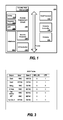
- FIG. 1 is a block diagram depicting a system-on-chip (SOC) including access enablement circuitry.
- SOC system-on-chip
- FIG. 2 is a flowchart describing a process for generating a SoC design including access enablement circuitry.
- FIG. 3 is a block diagram depicting an access enablement table in accordance with one embodiment.
- FIG. 4 is a block diagram depicting the generation of a SoC design having access enablement circuitry defined by an access enablement table.
- FIG. 5 is a block diagram depicting a SoC design including access enablement circuitry.
- FIG. 6 is a block diagram depicting details of access enablement circuitry for an output signal.
- SoC's Systems-on-chip (SoC's) and related techniques for designing and manufacturing SoC's are provided.
- a centralized access enablement circuit controls access to a plurality of individual security features for a SoC, such as test, debug, and/or evaluation interfaces provided by the different modules of the system.
- the access enablement circuit provides a central location and design point for managing the various security features provided by the SoC. In this manner, the access enablement circuit provides a central location for enabling and disabling hardware within the system to control security features.
- a SoC in one embodiment defines different security states, providing irreversible progression through the security states as the chip is manufactured.
- the access enablement circuit for a SoC implementing different security states provides individual access control settings for the different security states. In this manner, each security feature can have an individual control setting for the different security states, allowing select features to be enabled for a given security state.
- One-time programmable memory and register controls are provided in one embodiment that allow different access control settings for an individual security feature.
- An access enablement table is provided that contains an implementation definition of the access enablement circuit for controlling the security features of a SoC.
- An access control setting for each individual security feature is provided in the table comprising one or more input parameters.
- the access enablement table provides a simple, understandable and centralized view of security control and access for the system.
- the table may provide security specific controls for each security feature, including the ability to control a feature as always on, always off, programmable with default on and off, and lockable, or a more complex function based on its inputs.
- a security feature may be defined based on a logical combination of settings for other security features.
- the access enablement table defines an access control setting for the security feature based on the security state of the SoC.
- a circuit design for the access enablement circuit is automatically generated from the access enablement table.
- the access enablement table is parsed into the components for generating a hardware description language (HDL) representation of the access enablement circuit.
- HDL hardware description language
- This can include parsing the table into one or more ROM components and an output signal list for the access enablement circuit in one example. The results of parsing are used to automatically generate the HDL for the access enablement circuit.
- Each output signal and ROM can be instantiated, along with adding connecting logic for the components.
- FIG. 1 illustrates an example of a system-on-chip (SoC) 200 having an access enablement circuit in accordance with one or more embodiments.
- SoC 200 includes one or more interfaces 202 that expose debug, test and/or evaluation features within the SoC. Collectively, these features are referred to as security features.
- Interfaces 202 may include one or more pins used as a port or otherwise for external communication with SoC 200 .
- interfaces 202 may expose security features such DFT JTAG tap controllers, DFT P1500 Tap controllers, DFT test features such as scan dump, memory dump, memory BIST, JTAG SW debuggers for embedded processors, JTAG bridges to on-chip busses, on-chip debug bus logic, security fences, voltage glitch detection circuits/level monitors, clock glitch detection circuits/level monitors, temperature monitors, input/output (I/O) signal glitch catcher circuits, digital and analog debug busses, digital and analog test busses, bypass, clock enables, PLL test circuits, general purpose I/O's, on-chip clock stop circuitry, clock controls, reset controls, test busses, input/output (I/O) pads, DFT features, or any other security components for which access is to be controlled.
- security features such as DFT JTAG tap controllers, DFT P1500 Tap controllers, DFT test features such as scan dump, memory dump, memory BIST, JTAG SW debuggers for embedded processors,
- System on chip 200 includes a host processor 212 , an input/output (I/O) controller 214 , a memory controller 216 , and a security processor 218 that can communicate with one another via a bus 220 .
- the system bus 220 may be any of several types of bus structures including a memory bus or memory controller, a peripheral bus, and a local bus using any of a variety of bus architectures.
- bus architectures include Industry Standard Architecture (ISA) bus, Micro Channel Architecture (MCA) bus, Enhanced ISA (EISA) bus, Video Electronics Standards Association (VESA) local bus, and Peripheral Component Interconnect (PCI) bus also known as Mezzanine bus, and the Advanced Microcontroller Bus Architecture (AMBA) bus.
- DMA controllers which route data directly between external interfaces and memory, bypassing the processor core and thereby increasing the data throughput of the SoC can also be used.
- FIG. 1 it is to be appreciated that additional or fewer components can be included in system-on-chip 200 .
- additional controllers or processors can be included, cache memories can be included, multiple security processors 218 can be included, and so forth.
- a stand-alone security processor 218 is not included in SoC 200 .
- security processing may be provided by host processor 212 .
- Memory controller 216 controls access to and operations for memory 222 .
- Memory 222 can include volatile media (such as random access memory (RAM)) and/or nonvolatile media (such as read only memory (ROM), Flash memory, and so forth).
- Memory controller 216 allows different components of system on chip 200 , such as host processor 212 and security processor 218 , to write to and/or read from memory 222 .
- Data and/or instructions can be read from and/or written to memory 222 , such as instructions of a program to be executed by security processor 218 or host processor 212 , data for a program being executed by security processor 218 or host processor 212 , and so forth.
- Host processor 212 executes one or more programs that provide various functionality of device 200 , such as audio and/or video recording and/or playback, gaming and/or other recreational functions, and so forth.
- I/O controller 214 allows one or more external components or devices to communicate with components or modules of device 200 .
- I/O controller 214 operates in a conventional manner to identify signals received via the pins or other connection mechanism of external interfaces 202 , and to detect signal values based on the identified signals. These signals can be, for example, changes in voltage levels that indicate digital values of 0 or digital values of 1.
- I/O controller 214 provides the detected signal value to another component of system on chip 204 , typically host processor 212 or security processor 218 .
- Security processor 218 executes one or more programs that provide security functionality for system on chip 200 .
- This security functionality can include, for example, encryption and/or decryption of data, verifying digital signatures of instructions (e.g., programs or modules) that are included in memory 222 so that only verified instructions are executed by security processor 218 and/or host processor 212 , and so forth.
- Access enablement circuit (AEC) 230 is a centralized circuit that controls access to the individual security features of SoC 200 , for example, as may be exposed over interfaces 202 .
- AEC 230 provides individual control of each security specific feature of SoC 200 from a centralized location. For each security feature, the AEC 230 controls the feature as always enabled, always disabled, programmable by security processor 218 or other component, with default on or off, and lockable. The AEC 230 may also control the feature using a complex function based on inputs for the security feature.
- a lockable security feature is one where the security processor 218 or other component can enable or disable the feature, but then cannot further modify the feature for a current power cycle of the part.
- AEC 230 provides and controls an output for controlling each security feature of the SoC 200 .
- Each output can include a wire or subset of wires in the circuit that control a particular security feature.
- logic may be used at the destination to determine the state of enablement.
- a set of security states for SoC 200 are defined using one-time programmable security state memory 204 , such as programmable fuses, to enable different security feature sets for a part at different times in one embodiment.
- the set of security states and a pre-defined progression through them can be defined by blowing or otherwise programming the memory 204 as the part undergoes manufacturing, testing, and then is provided to an end-user.
- One embodiment provides a set of security states with each security state having a particular set of behaviors defined for the set of security features. For each security state, the individual security features may be enabled, disabled, have a default setting with software programmability, and/or the ability to be locked. In this manner, each security state may be defined with a different set of available security features.
- the security states have a defined irreversible progression as the part is manufactured.
- the part may have an initial or blank state defined for its manufacturing phase.
- the access enablement circuitry may generally provide access to many of the security features.
- the initial blank state may disable many security features, for example, to prevent exposures to security states being glitched to a blank state with voltage attacks and thereby exposing security features.
- the AEC 230 may also limit access to various functional elements at this stage. After manufacturing, the fuses may be programmed to a different encoding defining a test security state. In the test security state, for example, the AEC 230 may generally provide access to most security features and functional features.
- an operational security state may be programmed into the fuses. In this state, most security features may be disabled while most or all functional elements are enabled. As noted above and described hereinafter, software programmability and other means may be used to control the behavior for a security feature, rather than only defining an enabled or disabled condition.
- Access enablement circuitry 230 includes or accesses ROM's 232 in one embodiment to further control individual security features.
- the AEC 230 may define a default access control for a security feature using a first ROM and define the influence of software on the security feature using a second ROM.
- other memories can be used to define access control settings and software influences.
- programmable fuses or SRAM loaded from a software table may be used.
- AEC 230 additionally includes or accesses a set of data registers 234 in one embodiment. The data registers can be modified by software and/or the security processor 218 in one embodiment to enable, disable, and/or lock a corresponding security feature. The AEC may read the set of data registers to determine an access control setting for a security feature.
- AEC 230 includes or accesses a set of one-time programmable fuses 236 in one embodiment that provide additional control over security features.
- the OTP fuses may permit the same security feature to have a different behavior based on the OTP bits. In this manner, the OTP fuses can be programmed after manufacture to alter the access control setting for a security feature.
- FIG. 2 is a flowchart describing a method of manufacturing a SoC including an access enablement circuit in accordance with an embodiment.
- an access enablement table is accessed that fully describes the hardware behavior for the access enablement circuit.
- the AEB table includes entries for each output of the AEC, setting the behavior of each output for each mode and security state of the chip.
- the AEB table is parsed using an automated script to generate the components for the AEC.
- the table is parsed into the components for an HDL description of the AEC.
- the components may include ROM's that define the output behaviors of the output signals of the AEC for controlling the security features of the chip.
- an HDL description of the AEC circuit is generated.
- generating the HDL description may include instantiate each output signal of the AEC, instantiating each ROM, and adding connecting logic to define how the ROM data is utilized to control the behavior of each output signal.
- SoC's are manufactured using the generated HDL description of the AEC.
- the ROM based implementation permits changes to the ROM contents simply by altering the AEB table. This permits changes to the AEC design in subsequent silicon revisions without significant digital or physical design impacts.
- FIG. 3 is a block diagram describing an example of an access enablement table according to one embodiment.
- the AEB table forms the complete basis for a hardware description (HDL) implementation of an access enablement circuit in one embodiment.
- the AEB table is provided as a spreadsheet in one example, containing the implementation definition for the security features of the SoC. Each security feature is set forth as a row in the spreadsheet under the “Output” heading.
- the complete access enablement definition for a security feature includes several parameters set forth as the columns in the spreadsheet. When combined, the features in the column define access control to the security feature in all implementation aspects.
- the security features include a “Clock” security feature which can be used to gate clocks or select signals for clock muxes to provide secured clock gating or switching.
- a “Reset” security feature can be used to either issue a reset or mask a reset issued by other less trusted entities.
- a “Debug” security feature controls access to on-chip debug circuits.
- An “I/O Pads” security feature controls access to I/O pads of the chip for enablement or configuration purposes.
- a “Bus Interface” security feature controls access to certain client on a given bus or an entire bus interface.
- a “DFT” security feature controls access to DFT features such as scan, MBIST, memory dump, scan dump, and boundary scan.
- the depicted security features are provided by way of example only. Different SoC implementations may include different security features than those depicted in FIG. 3 .
- a first column of the AEB table corresponds to a first security state of the chip as programmed in the set of fuses 204 .
- the first security state column sets forth the security behavior for each of the security features when the chip is in the first security state.
- the “Clock” security feature is set to HWNO.
- the HWNO access control setting indicates that the “Clock” security feature is hardware disabled when the chip is in the first security state.
- the AEC generated from the table will generate an output in the first security state that disables or otherwise prevents access to clock gating and switching.
- the “Reset” security feature is set to HWYES.
- the HWYES access control setting indicates that for the first security state, the “Reset” feature or ability to issue a reset or mask a reset is always hardware-enabled.
- the control settings for the remaining security features for the first security state are set forth with either HWYES or HWNO designations.
- a second column of the AEB table corresponds to a second security state of the chip.
- the “Clock” security feature is set to HWYES as earlier described.
- the “Reset,” “Debug” and “Test Circuit” security features are each set to Y/SPWL.
- the “Y” access control setting designates that the security feature is enabled by default when in the second security state.
- the additional SPWL designation defines the security feature as “Security Processor Write Locked.”
- the AEB table sets forth that the security processor may disable the feature from its default enabled setting, and optionally also lock the feature from being enabled for the current boot cycle.
- the “I/O Pads,” “Bus Interface,” and “DFT” security features are each set to N/SPWL.
- the “N” access control setting sets forth that the security feature is disabled by default.
- the additional SPWL access control setting in conjunction with the default “N” access control setting, sets forth that the security processor may enable the feature, and optionally also disable it again and lock it from being enabled again for the current boot cycle.
- the access control setting for a security feature can also be based on the access control setting of one or more other security features. For example, it may be determined that for a certain combination of enabled security features, another security feature should have a particular setting. Accordingly, the entry for such a feature in a given security state may be defined by the access control settings for one or more other security settings in that security state.
- the AEB table may include an additional column with an index list. The table entry for a feature can then be based on a logical combination of index lookups from other features in the table.
- the table entry for a security feature may be based on state logic from any other location within the table. For example, the entry may be a logical combination of the outputs of other rows.
- the security feature entry may be a logical combination of the inputs for one or more other entries in the table. Such rows may be defined as custom rows. An equation can be defined for a row based on any input, or logic from another row.
- the AEB table in FIG. 3 has several optional columns that permit further control over the security features of the SoC.
- the OTP column permits a particular security feature to have different behaviors or access control under the same security state. If a “1” is set forth in the column for a security feature, the security feature can be controlled by data from a one-time programmable (OTP) memory. In this manner, one or more OTP bits can be programmed after the chip is designed and manufactured to change the access control for a security feature when under a particular security state.
- OTP one-time programmable
- the “Clock” security feature may have a default access control of “HWNO” when the corresponding OTP bit is not programmed, for example binary “0.” If the corresponding OTP bit is programmed, for example to binary “1,” the AEC circuitry may permit access to the “Clock” security feature.
- the REV_SEL column allows certain features to have an override for one or more revisions for the chip manufacture. For example, a new “test circuit” or other circuit may be provided in a chip as a prototype or otherwise as a completely untested component whose behavior cannot be guaranteed.
- the REV_SEL designation allows the feature to be bypassed for a first or subsequent silicon revision of the chip. For example, if the new circuit does not work or perform in a manner consistent with the SoC operation, the REV_SEL designation permits an override of the feature during the revision of the current revision and optionally subsequent revisions of the silicon.
- the table may be extended in other manners to take any input from the SoC.
- the AEB table may include additional rows that are implemented as spares in the AEC implementation.
- an additional spare row can include the most commonly used ROM implementations.
- the spare rows can be connected to minimize design changes. Furthermore, this enables independent control over a security feature that may have not been enabled for control in an earlier silicon revision.
- FIG. 4 is a block diagram depicting the generation of a hardware description language (HDL) description for an access enablement circuit according to one embodiment.
- An access enablement table 300 is provided including a plurality of rows corresponding to a set of security features for a SoC, and a plurality of columns corresponding to a set of security states for the SoC. As described with respect to FIG. 2 , the table can include additional columns corresponding to registers, programmable memory, or revision select signals for example.
- the table fully describes the hardware behavior of each output of an access enablement circuit for all modes and/or security-states of the SoC's operation. Each entry in the table corresponds to an output signal generated by the AEC. Each output signal will have a defined behavior based on the inputs for the entry, including for example, the security state of the chip, a software register interface, and/or one-time programmable memory bits as earlier described.
- An automated script first parses the AEB table and checks for any syntax errors or omissions at block 305 . If there is a syntax or omission failure, the table is rejected so that user edits and/or updates can be applied at block 315 .
- the automated script parses the AEB table to generate AEB parsing results 320 .
- the parsing results 320 include an output signal list 322 including the outputs for access control of each security feature.
- the script extracts the behavior for each output signal for all modes and security states of operation.
- the script generates a description for one or more ROM's that define the output behaviors of the output signals. Each ROM is a two-dimensional array that defines the total set of behaviors for the AEC.
- one dimension of the ROM correlates to the number of security states of the SoC and the other dimension of the ROM correlates to the number of output signals for the AEC.
- Each entry in each ROM includes a binary value that encodes information relating to the output signal's behavior in a particular security state.
- the example of FIG. 4 includes two ROM's , ROM-A and ROM-B.
- ROM-A and ROM-B When the output signals of an AEC are defined by multiple inputs with different behavioral impacts, more than one ROM can be generated, with each ROM defining an individual component of the signal's output behavior.
- a first ROM defines the default behavior of each output signal while a second ROM defines whether each output signal can be influenced by software modifiable registers.
- a set of ROM parity check values are also generated from the table.
- the automated script calculates a hash value of the table binary at step 310 .
- the table hash value is recorded at box 360 .
- the hash value is recorded to provision revision control to make sure that which is fabricated from HDL is the same as the source AEB table.
- the script After generating the AEB parsing results 320 , the script automatically generates an HDL description for the AEC implementation. In one embodiment, the script instantiates each output signal and each ROM from the parsing results. The script also adds connection logic for combining inputs from the ROM(s), registers, OTP bits, etc. Optionally, the script can instantiate the ROM parity output from the parsing results to protect against silicon defects and/or silicon modification attacks (e.g., focused ion beam (FIB)).
- FIB focused ion beam
- FIG. 5 is block diagram of an example of a circuit implementation in accordance with one embodiment.
- ROM-B 404 defines a default state of each output signal and ROM-A defines an influence of a set of software modifiable registers on each output signal.
- ROM-based approach allows for late changes to the ROM contents via late changes to the AEB table. Because of the ROMs, the changes do not cause significant digital or physical design impact.
- the ROMs can be changed for subsequent silicon revisions using a single metal layer spin. In other ROM implementations, additional metal layers may be used.
- ROM-B For each security state, ROM-B generates an output for each security feature indicating the default state of the security feature, such as hardware-enabled, hardware-disabled, etc.
- ROM-B is a two-dimensional array with a first dimension equal to a number of security states (State1-StateX) and a second dimension equal to a number N of security features (N).
- State1-StateX security states
- N security features
- the outputs of ROM-B are communicated to a multiplexor 410 which receives as a selection input the active security state from the set of programmable fuses.
- the multiplexor selects a set of outputs from ROM-B based on the active security state.
- the multiplexor communicates with user-defined connection logic 415 to provide a set of outputs from ROM-B based on the active security state.
- ROM-A For each security state, ROM-A generates an output for each security feature indicating whether the security feature is modifiable by software.
- the outputs of ROM-A are communicated to a multiplexor 425 which receives the active security state as a selection input.
- the multiplexor selects and communicates to user-defined connection logic 420 a set of outputs from ROM-A based on the active security state.
- the connection logic 420 receives the output signals for the active security state and also a register file or other input from the set of software modifiable data registers.
- the register data includes an input for each security feature. Based on the input from multiplexor 425 , connection logic 420 determines whether to use the register data. The connection logic chooses whether to use the register data for each security feature individually.
- connection logic provides an output signal for each security feature based on the active security state.
- the user-defined connection logic may be unique for each output signal.
- the connection logic may provide a generic set of connection logic or custom connection logic for other output signals.
- Some output signals may include security sensitive custom connection logic, for example implementing voltage-attack-resistant (VAR) macros, and similar hardware to protect against security attacks.
- VAR voltage-attack-resistant
- FIG. 6 is a block diagram depicting connection logic 415 and 420 in one example. A portion of the connection logic for a single output of the access enablement circuit is depicted. The connection logic may be replicated “N” times to generate an output signal for each security feature or entry in the AEB table.
- register file 435 includes a set of three registers for each output signal. The registers include an “enable” (EN) register, a “disable” (DI) register, and a “write-lock disable” (WL) register.
- each register provides a single bit to the connection logic 420 .
- a read-only “status” register may be provided to feedback the state of the output signals for software checking.
- ROM-B provides a default access control setting (DF) to the connection logic for the security feature.
- ROM-A provides a register override enable (RO) signal indicating whether the register data is to be used for the output signal. If the RO signal is asserted, the register data will override the DF setting. Otherwise, the register data will be ignored.
- the connection logic implements IF/ELSE logic based on the output of ROM-A. First, the connection logic determines whether the register override enable is provided from ROM-A for the security feature. If the RO signal is de-asserted, the connection logic sets the output signal (OT) to the default state DF.
- the connection logic executes the ELSE statement including a set of case statements based on the enable register value, the disable register value, and the write-lock disable register value. In this case, if all three registers provide a binary ‘0,’ the connection logic sets the output signal to the default state DF, either enabled or disabled. If the write-lock disable register provides a binary ‘1,’ the connection logic sets the output signal to the ‘0,’ indicating that the security feature is disabled. If the write-lock disable register provides a binary ‘0,’ and the disable register provides a binary ‘1,’ the connection logic sets the output signal to ‘0,’ indicating that the security feature is disabled. If the write-lock disable and disable registers are both set to ‘0’ and the enable register is set to ‘1,’ the connection logic sets the output signal to ‘1’ indicating that the security feature is enabled.
- Computer readable media can be any available media that can be accessed by a computing device and includes both volatile and nonvolatile media, removable and non-removable media.
- Computer readable media may comprise computer readable storage media and communication media.
- Computer readable storage media includes volatile and nonvolatile, as well as removable and non-removable media implemented in any method or technology for storage of information such as computer readable instructions, data structures, program modules or other data.
- Computer readable storage media includes, but is not limited to, random access memory (RAM), read only memory (ROM), EEPROM, flash memory or other memory technology, CD-ROMs, digital versatile discs (DVDs) or other optical disc storage, magnetic cassettes, magnetic tapes, magnetic disc storage or other magnetic storage devices, or any other medium which can be used to store the information and which can be accessed by a computing device.
- Communication media typically embodies computer readable instructions, data structures, program modules or other data in a modulated data signal such as a carrier wave or other transport mechanism and includes any information delivery media.
- modulated data signal means a signal that has one or more of its characteristics set or changed in such a manner as to encode information in the signal.
- communication media includes wired media such as a wired network or direct-wired connection, and wireless media such as RF and other wireless media. Combinations of any of the above are also included within the scope of computer readable media.
- a system-on-chip that comprises a plurality of hardware modules implemented on a silicon substrate and that are configured for communication over one or more buses.
- the plurality of hardware modules provide a plurality of security features.
- the SoC includes a set of programmable fuses defining a progression of a plurality of security states for the system-on-chip and at least one read only memory (ROM) defining an access control setting for each security feature in each security state.
- a centralized access enablement (AEB) circuit of the SoC is provided for controlling access to the plurality of security feature.
- the centralized AEB circuit includes a plurality of outputs. Each output corresponds to a security feature of the hardware modules and controls access to the security feature.
- the AEB circuit generates each output based on an output of the at least one ROM for an active security state.
- a computer-implemented method of system-on-chip design that comprises generating an access enablement table for a plurality of security features of a system-on-chip (SoC).
- the access enablement table includes for each security feature a plurality of access control settings corresponding to a plurality of security states of the SoC.
- the method includes automatically parsing the access enablement table to generate one or more components for describing an access enablement circuit to control the plurality of security feature of the SoC, and automatically generating a hardware description of the access enablement circuit from the one or more components.
Abstract
Description
Claims (27)
Priority Applications (1)
| Application Number | Priority Date | Filing Date | Title |
|---|---|---|---|
| US14/013,561 US9436844B2 (en) | 2013-08-29 | 2013-08-29 | Access enablement security circuit |
Applications Claiming Priority (1)
| Application Number | Priority Date | Filing Date | Title |
|---|---|---|---|
| US14/013,561 US9436844B2 (en) | 2013-08-29 | 2013-08-29 | Access enablement security circuit |
Publications (2)
| Publication Number | Publication Date |
|---|---|
| US20150067771A1 US20150067771A1 (en) | 2015-03-05 |
| US9436844B2 true US9436844B2 (en) | 2016-09-06 |
Family
ID=52585202
Family Applications (1)
| Application Number | Title | Priority Date | Filing Date |
|---|---|---|---|
| US14/013,561 Active US9436844B2 (en) | 2013-08-29 | 2013-08-29 | Access enablement security circuit |
Country Status (1)
| Country | Link |
|---|---|
| US (1) | US9436844B2 (en) |
Cited By (2)
| Publication number | Priority date | Publication date | Assignee | Title |
|---|---|---|---|---|
| US10862704B2 (en) | 2019-03-07 | 2020-12-08 | Nxp Usa, Inc. | Time-based secure access control system |
| US10936771B1 (en) | 2019-10-02 | 2021-03-02 | Microsoft Technology Licensing, Llc | Using a common fuse controller hardware design for different applications |
Families Citing this family (4)
| Publication number | Priority date | Publication date | Assignee | Title |
|---|---|---|---|---|
| CN108073831B (en) * | 2016-11-15 | 2020-07-24 | 华为技术有限公司 | Method for detecting working state of safety chip and detection circuit |
| CN112770318B (en) * | 2019-11-01 | 2022-11-18 | 苏州千米电子科技有限公司 | Terminal registration method and device |
| WO2022100812A1 (en) * | 2020-11-10 | 2022-05-19 | Zf Cv Systems Global Gmbh | Integrated circuit, method for operating the integrated circuit, computer program product, electronic control unit and vehicle |
| CN112444735B (en) * | 2020-11-27 | 2023-06-13 | 成都海光集成电路设计有限公司 | Chip capable of being configured safely and operation method thereof |
Citations (29)
| Publication number | Priority date | Publication date | Assignee | Title |
|---|---|---|---|---|
| US20040025010A1 (en) | 2002-07-30 | 2004-02-05 | Texas Instruments Incorporated | Computing platform certificate |
| US6980239B1 (en) * | 2001-10-19 | 2005-12-27 | Pixim, Inc. | Imaging system with multiple boot options |
| US20070209072A1 (en) | 2006-02-27 | 2007-09-06 | Xuemin Chen | Method and system for secure system-on-a-chip architecture for multimedia data processing |
| US7310721B2 (en) | 2003-10-30 | 2007-12-18 | Microsoft Corporation | Shadow page tables for address translation control |
| US20080148343A1 (en) | 2006-12-19 | 2008-06-19 | International Business Machines Corporation | Debugging security mechanism for soc asic |
| US20080263362A1 (en) | 2007-04-17 | 2008-10-23 | Chen Xuemin Sherman | Method and apparatus of secure authentication for system on chip (soc) |
| US20080282087A1 (en) | 2007-05-11 | 2008-11-13 | Mips Technologies, Inc. | System debug and trace system and method, and applications thereof |
| US20090296933A1 (en) * | 2004-11-22 | 2009-12-03 | Freescale Semiconductor, Inc. | Integrated circuit and a method for secure testing |
| US20100005314A1 (en) | 2003-05-30 | 2010-01-07 | Johnson Barry W | In-circuit security system and methods for controlling access to and use of sensitive data |
| US20100106899A1 (en) | 2006-09-29 | 2010-04-29 | Broadcom Corporation | Global address space management |
| US7742597B2 (en) | 2007-12-28 | 2010-06-22 | Lewis James M | Exclusive encryption system |
| US7822993B2 (en) | 2004-08-27 | 2010-10-26 | Microsoft Corporation | System and method for using address bits to affect encryption |
| US20110066835A1 (en) | 2009-09-14 | 2011-03-17 | Love Kothari | Method and system for securely protecting a semiconductor chip without compromising test and debug capabilities |
| US8037437B2 (en) | 2009-01-13 | 2011-10-11 | Microsoft Corporation | Optimizing systems-on-a-chip using the dynamic critical path |
| US20110302577A1 (en) | 2010-06-02 | 2011-12-08 | Microsoft Corporation | Virtual machine migration techniques |
| US20120082171A1 (en) | 2003-07-25 | 2012-04-05 | Microsoft Corporation | Single chip protocol converter |
| US20120137119A1 (en) * | 2010-10-15 | 2012-05-31 | Doerr Michael B | Disabling Communication in a Multiprocessor System |
| US8195914B2 (en) | 2002-12-27 | 2012-06-05 | Intel Corporation | Mechanism for remapping post virtual machine memory pages |
| US8255578B2 (en) | 2010-06-14 | 2012-08-28 | Microsoft Corporation | Preventing access to a device from an external interface |
| US8255700B2 (en) | 2004-06-29 | 2012-08-28 | Qualcomm Incorporated | Lockstep mechanism to ensure security in hardware at power-up |
| US8285980B1 (en) | 2006-12-18 | 2012-10-09 | Marvell International Ltd. | System-on-a-chip (SoC) security using one-time programmable memories |
| US20130022201A1 (en) | 2011-07-19 | 2013-01-24 | Gerrity Daniel A | Encrypted memory |
| US20130086385A1 (en) | 2011-09-30 | 2013-04-04 | Yuri Poeluev | System and Method for Providing Hardware-Based Security |
| US20130205139A1 (en) | 2010-10-05 | 2013-08-08 | Craig A. Walrath | Scrambling An Address And Encrypting Write Data For Storing In A Storage Device |
| US20130212382A1 (en) | 2011-01-14 | 2013-08-15 | Netauthority, Inc. | Device-bound certificate authentication |
| US20130290286A1 (en) * | 2012-04-27 | 2013-10-31 | Huawei Technologies Co., Ltd. | Method, apparatus, and system for operating shared resource in asynchronous multiprocessing system |
| US20140108825A1 (en) | 2008-11-24 | 2014-04-17 | Certicom Corp. | System and Method for Hardware Based Security |
| US20140359755A1 (en) * | 2013-05-30 | 2014-12-04 | Cryptography Research, Inc. | Configurator for secure feature and key manager |
| US20150095661A1 (en) | 2013-09-30 | 2015-04-02 | Microsoft Corporation | Flexible Memory Addressing For Data Security |
-
2013
- 2013-08-29 US US14/013,561 patent/US9436844B2/en active Active
Patent Citations (30)
| Publication number | Priority date | Publication date | Assignee | Title |
|---|---|---|---|---|
| US6980239B1 (en) * | 2001-10-19 | 2005-12-27 | Pixim, Inc. | Imaging system with multiple boot options |
| US20040025011A1 (en) | 2002-07-30 | 2004-02-05 | Jerome Azema | Secure management of configuration parameters in a computing platform |
| US20040025010A1 (en) | 2002-07-30 | 2004-02-05 | Texas Instruments Incorporated | Computing platform certificate |
| US8195914B2 (en) | 2002-12-27 | 2012-06-05 | Intel Corporation | Mechanism for remapping post virtual machine memory pages |
| US20100005314A1 (en) | 2003-05-30 | 2010-01-07 | Johnson Barry W | In-circuit security system and methods for controlling access to and use of sensitive data |
| US20120082171A1 (en) | 2003-07-25 | 2012-04-05 | Microsoft Corporation | Single chip protocol converter |
| US7310721B2 (en) | 2003-10-30 | 2007-12-18 | Microsoft Corporation | Shadow page tables for address translation control |
| US8255700B2 (en) | 2004-06-29 | 2012-08-28 | Qualcomm Incorporated | Lockstep mechanism to ensure security in hardware at power-up |
| US7822993B2 (en) | 2004-08-27 | 2010-10-26 | Microsoft Corporation | System and method for using address bits to affect encryption |
| US20090296933A1 (en) * | 2004-11-22 | 2009-12-03 | Freescale Semiconductor, Inc. | Integrated circuit and a method for secure testing |
| US20070209072A1 (en) | 2006-02-27 | 2007-09-06 | Xuemin Chen | Method and system for secure system-on-a-chip architecture for multimedia data processing |
| US20100106899A1 (en) | 2006-09-29 | 2010-04-29 | Broadcom Corporation | Global address space management |
| US8285980B1 (en) | 2006-12-18 | 2012-10-09 | Marvell International Ltd. | System-on-a-chip (SoC) security using one-time programmable memories |
| US20080148343A1 (en) | 2006-12-19 | 2008-06-19 | International Business Machines Corporation | Debugging security mechanism for soc asic |
| US20080263362A1 (en) | 2007-04-17 | 2008-10-23 | Chen Xuemin Sherman | Method and apparatus of secure authentication for system on chip (soc) |
| US20080282087A1 (en) | 2007-05-11 | 2008-11-13 | Mips Technologies, Inc. | System debug and trace system and method, and applications thereof |
| US7742597B2 (en) | 2007-12-28 | 2010-06-22 | Lewis James M | Exclusive encryption system |
| US20140108825A1 (en) | 2008-11-24 | 2014-04-17 | Certicom Corp. | System and Method for Hardware Based Security |
| US8037437B2 (en) | 2009-01-13 | 2011-10-11 | Microsoft Corporation | Optimizing systems-on-a-chip using the dynamic critical path |
| US20110066835A1 (en) | 2009-09-14 | 2011-03-17 | Love Kothari | Method and system for securely protecting a semiconductor chip without compromising test and debug capabilities |
| US20110302577A1 (en) | 2010-06-02 | 2011-12-08 | Microsoft Corporation | Virtual machine migration techniques |
| US8255578B2 (en) | 2010-06-14 | 2012-08-28 | Microsoft Corporation | Preventing access to a device from an external interface |
| US20130205139A1 (en) | 2010-10-05 | 2013-08-08 | Craig A. Walrath | Scrambling An Address And Encrypting Write Data For Storing In A Storage Device |
| US20120137119A1 (en) * | 2010-10-15 | 2012-05-31 | Doerr Michael B | Disabling Communication in a Multiprocessor System |
| US20130212382A1 (en) | 2011-01-14 | 2013-08-15 | Netauthority, Inc. | Device-bound certificate authentication |
| US20130022201A1 (en) | 2011-07-19 | 2013-01-24 | Gerrity Daniel A | Encrypted memory |
| US20130086385A1 (en) | 2011-09-30 | 2013-04-04 | Yuri Poeluev | System and Method for Providing Hardware-Based Security |
| US20130290286A1 (en) * | 2012-04-27 | 2013-10-31 | Huawei Technologies Co., Ltd. | Method, apparatus, and system for operating shared resource in asynchronous multiprocessing system |
| US20140359755A1 (en) * | 2013-05-30 | 2014-12-04 | Cryptography Research, Inc. | Configurator for secure feature and key manager |
| US20150095661A1 (en) | 2013-09-30 | 2015-04-02 | Microsoft Corporation | Flexible Memory Addressing For Data Security |
Non-Patent Citations (9)
| Title |
|---|
| "Discretix Secure Debug Module (DxSDM)", Retrieved on: Apr. 29, 2013, Available at: http://www.discretix.com/Products-Solutions/Secure-Debug.html. |
| "Security Model for the Next-Generation Secure Computing Base," Published on: Feb. 6, 2004, Available at: http://www.microsoft.com/resources/ngscb/documents/NGSCB-Security-Model.doc. |
| Akselrod, et al., "Platform Independent Debug Port Controller Architecture with Security Protection for Multi-Processor System-on-Chip ICs", In Proceedings of the Conference on Design, Automation and Test in Europe: Designers' Forum, Mar. 6, 2006, 6 pages. |
| Altmark, Alan, "Understanding z/VM Integrity and Security," Published on: Nov. 2002, Available at: http://www.ibmsystemsmag.com/mainframe/administrator/security/Understanding-z-VM-Integrity0and-Security/?page=2. |
| Fujiyama, Hiroyuki, "System-on-a-Chip with Security Modules for Network Home Electric Appliances," Fujitsu Sci. Tech. J., vol. 42, No. 2, Apr. 2006, pp. 227-233. |
| Li, et al., "Secure Virtual Machine Execution under an Untrusted Management OS," In IEEE 3rd International Conference on Cloud Computing, Jul. 5, 2010, 8 pages. |
| Non-final Office Action dated Jan. 2, 2015, U.S. Appl. No. 14/026,804, filed Sep. 13, 2013. |
| Suh, et al., "Efficient Memory Integrity Verification and Encryption for Secure Processors," In Proceedings of the 36th Annual International Symposium on Microarchitecture, Dec. 2003, 15 pages. |
| U.S. Appl. No. 14/026,804, filed Sep. 13, 2013. |
Cited By (2)
| Publication number | Priority date | Publication date | Assignee | Title |
|---|---|---|---|---|
| US10862704B2 (en) | 2019-03-07 | 2020-12-08 | Nxp Usa, Inc. | Time-based secure access control system |
| US10936771B1 (en) | 2019-10-02 | 2021-03-02 | Microsoft Technology Licensing, Llc | Using a common fuse controller hardware design for different applications |
Also Published As
| Publication number | Publication date |
|---|---|
| US20150067771A1 (en) | 2015-03-05 |
Similar Documents
| Publication | Publication Date | Title |
|---|---|---|
| US9716708B2 (en) | Security certificates for system-on-chip security | |
| US9436844B2 (en) | Access enablement security circuit | |
| US11948652B2 (en) | Formal verification tool to verify hardware design of memory unit | |
| US9471785B2 (en) | Systems and methods for secure boot ROM patch | |
| US7152193B2 (en) | Embedded sequence checking | |
| US10496506B2 (en) | Self-test capable integrated circuit apparatus and method of self-testing an integrated circuit | |
| US8438436B1 (en) | Secure design-for-test scan chains | |
| US9224012B2 (en) | Debug functionality in a secure computing environment | |
| US11023623B2 (en) | Method for triggering and detecting a malicious circuit in an integrated circuit device | |
| TWI405125B (en) | Apparatus and method for updating set of limited access model specific registers in a microprocessor | |
| US20140344960A1 (en) | Selective control of on-chip debug circuitry of embedded processors | |
| US20210150031A1 (en) | Verifying firmware binary images using a hardware design and formal assertions | |
| US11688486B2 (en) | Retention voltage management for a volatile memory | |
| KR101532363B1 (en) | Semiconductor device with multi acess level and access controlling method thereof | |
| US9817601B1 (en) | Method and apparatus for determining feasibility of memory operating condition change using different back bias voltages | |
| US10169177B1 (en) | Non-destructive online testing for safety critical applications | |
| Hu et al. | Imprecise security: quality and complexity tradeoffs for hardware information flow tracking | |
| US20170278583A1 (en) | Fusebox-based memory repair | |
| US9009457B2 (en) | Integrated circuit boot code and fuse storage implemented on interposer-mounted non-volatile memory | |
| US20170262384A1 (en) | Method for protecting memory against unauthorized access | |
| US8661302B2 (en) | Enhanced debug/test capability to a core reset process | |
| US9589088B1 (en) | Partitioning memory in programmable integrated circuits | |
| US9672094B1 (en) | Interconnect circuitry fault detection | |
| Kafka et al. | FPGA-based fault simulator | |
| US8242805B1 (en) | Method and apparatus for restricting the use of integrated circuits |
Legal Events
| Date | Code | Title | Description |
|---|---|---|---|
| AS | Assignment |
Owner name: MICROSOFT CORPORATION, WASHINGTON Free format text: ASSIGNMENT OF ASSIGNORS INTEREST;ASSIGNORS:LOVE, MICHAEL;ROBB, WALKER;CHHODAVDIA, AVDHESH;AND OTHERS;SIGNING DATES FROM 20130823 TO 20130826;REEL/FRAME:031112/0814 |
|
| AS | Assignment |
Owner name: MICROSOFT TECHNOLOGY LICENSING, LLC, WASHINGTON Free format text: ASSIGNMENT OF ASSIGNORS INTEREST;ASSIGNOR:MICROSOFT CORPORATION;REEL/FRAME:034747/0417 Effective date: 20141014 Owner name: MICROSOFT TECHNOLOGY LICENSING, LLC, WASHINGTON Free format text: ASSIGNMENT OF ASSIGNORS INTEREST;ASSIGNOR:MICROSOFT CORPORATION;REEL/FRAME:039025/0454 Effective date: 20141014 |
|
| STCF | Information on status: patent grant |
Free format text: PATENTED CASE |
|
| FEPP | Fee payment procedure |
Free format text: PAYOR NUMBER ASSIGNED (ORIGINAL EVENT CODE: ASPN); ENTITY STATUS OF PATENT OWNER: LARGE ENTITY |
|
| MAFP | Maintenance fee payment |
Free format text: PAYMENT OF MAINTENANCE FEE, 4TH YEAR, LARGE ENTITY (ORIGINAL EVENT CODE: M1551); ENTITY STATUS OF PATENT OWNER: LARGE ENTITY Year of fee payment: 4 |
|
| MAFP | Maintenance fee payment |
Free format text: PAYMENT OF MAINTENANCE FEE, 8TH YEAR, LARGE ENTITY (ORIGINAL EVENT CODE: M1552); ENTITY STATUS OF PATENT OWNER: LARGE ENTITY Year of fee payment: 8 |