US9235119B2 - Exposure photolithography methods - Google Patents
Exposure photolithography methods Download PDFInfo
- Publication number
- US9235119B2 US9235119B2 US14/457,149 US201414457149A US9235119B2 US 9235119 B2 US9235119 B2 US 9235119B2 US 201414457149 A US201414457149 A US 201414457149A US 9235119 B2 US9235119 B2 US 9235119B2
- Authority
- US
- United States
- Prior art keywords
- group
- aryl group
- radiation
- acid
- substituted aryl
- Prior art date
- Legal status (The legal status is an assumption and is not a legal conclusion. Google has not performed a legal analysis and makes no representation as to the accuracy of the status listed.)
- Expired - Fee Related
Links
Images


Classifications
-
- G—PHYSICS
- G03—PHOTOGRAPHY; CINEMATOGRAPHY; ANALOGOUS TECHNIQUES USING WAVES OTHER THAN OPTICAL WAVES; ELECTROGRAPHY; HOLOGRAPHY
- G03F—PHOTOMECHANICAL PRODUCTION OF TEXTURED OR PATTERNED SURFACES, e.g. FOR PRINTING, FOR PROCESSING OF SEMICONDUCTOR DEVICES; MATERIALS THEREFOR; ORIGINALS THEREFOR; APPARATUS SPECIALLY ADAPTED THEREFOR
- G03F7/00—Photomechanical, e.g. photolithographic, production of textured or patterned surfaces, e.g. printing surfaces; Materials therefor, e.g. comprising photoresists; Apparatus specially adapted therefor
- G03F7/004—Photosensitive materials
- G03F7/038—Macromolecular compounds which are rendered insoluble or differentially wettable
-
- G—PHYSICS
- G03—PHOTOGRAPHY; CINEMATOGRAPHY; ANALOGOUS TECHNIQUES USING WAVES OTHER THAN OPTICAL WAVES; ELECTROGRAPHY; HOLOGRAPHY
- G03F—PHOTOMECHANICAL PRODUCTION OF TEXTURED OR PATTERNED SURFACES, e.g. FOR PRINTING, FOR PROCESSING OF SEMICONDUCTOR DEVICES; MATERIALS THEREFOR; ORIGINALS THEREFOR; APPARATUS SPECIALLY ADAPTED THEREFOR
- G03F7/00—Photomechanical, e.g. photolithographic, production of textured or patterned surfaces, e.g. printing surfaces; Materials therefor, e.g. comprising photoresists; Apparatus specially adapted therefor
- G03F7/004—Photosensitive materials
- G03F7/0045—Photosensitive materials with organic non-macromolecular light-sensitive compounds not otherwise provided for, e.g. dissolution inhibitors
-
- G—PHYSICS
- G03—PHOTOGRAPHY; CINEMATOGRAPHY; ANALOGOUS TECHNIQUES USING WAVES OTHER THAN OPTICAL WAVES; ELECTROGRAPHY; HOLOGRAPHY
- G03F—PHOTOMECHANICAL PRODUCTION OF TEXTURED OR PATTERNED SURFACES, e.g. FOR PRINTING, FOR PROCESSING OF SEMICONDUCTOR DEVICES; MATERIALS THEREFOR; ORIGINALS THEREFOR; APPARATUS SPECIALLY ADAPTED THEREFOR
- G03F7/00—Photomechanical, e.g. photolithographic, production of textured or patterned surfaces, e.g. printing surfaces; Materials therefor, e.g. comprising photoresists; Apparatus specially adapted therefor
- G03F7/004—Photosensitive materials
- G03F7/0046—Photosensitive materials with perfluoro compounds, e.g. for dry lithography
-
- G—PHYSICS
- G03—PHOTOGRAPHY; CINEMATOGRAPHY; ANALOGOUS TECHNIQUES USING WAVES OTHER THAN OPTICAL WAVES; ELECTROGRAPHY; HOLOGRAPHY
- G03F—PHOTOMECHANICAL PRODUCTION OF TEXTURED OR PATTERNED SURFACES, e.g. FOR PRINTING, FOR PROCESSING OF SEMICONDUCTOR DEVICES; MATERIALS THEREFOR; ORIGINALS THEREFOR; APPARATUS SPECIALLY ADAPTED THEREFOR
- G03F7/00—Photomechanical, e.g. photolithographic, production of textured or patterned surfaces, e.g. printing surfaces; Materials therefor, e.g. comprising photoresists; Apparatus specially adapted therefor
- G03F7/004—Photosensitive materials
- G03F7/038—Macromolecular compounds which are rendered insoluble or differentially wettable
- G03F7/0382—Macromolecular compounds which are rendered insoluble or differentially wettable the macromolecular compound being present in a chemically amplified negative photoresist composition
-
- G—PHYSICS
- G03—PHOTOGRAPHY; CINEMATOGRAPHY; ANALOGOUS TECHNIQUES USING WAVES OTHER THAN OPTICAL WAVES; ELECTROGRAPHY; HOLOGRAPHY
- G03F—PHOTOMECHANICAL PRODUCTION OF TEXTURED OR PATTERNED SURFACES, e.g. FOR PRINTING, FOR PROCESSING OF SEMICONDUCTOR DEVICES; MATERIALS THEREFOR; ORIGINALS THEREFOR; APPARATUS SPECIALLY ADAPTED THEREFOR
- G03F7/00—Photomechanical, e.g. photolithographic, production of textured or patterned surfaces, e.g. printing surfaces; Materials therefor, e.g. comprising photoresists; Apparatus specially adapted therefor
- G03F7/004—Photosensitive materials
- G03F7/039—Macromolecular compounds which are photodegradable, e.g. positive electron resists
- G03F7/0392—Macromolecular compounds which are photodegradable, e.g. positive electron resists the macromolecular compound being present in a chemically amplified positive photoresist composition
-
- G—PHYSICS
- G03—PHOTOGRAPHY; CINEMATOGRAPHY; ANALOGOUS TECHNIQUES USING WAVES OTHER THAN OPTICAL WAVES; ELECTROGRAPHY; HOLOGRAPHY
- G03F—PHOTOMECHANICAL PRODUCTION OF TEXTURED OR PATTERNED SURFACES, e.g. FOR PRINTING, FOR PROCESSING OF SEMICONDUCTOR DEVICES; MATERIALS THEREFOR; ORIGINALS THEREFOR; APPARATUS SPECIALLY ADAPTED THEREFOR
- G03F7/00—Photomechanical, e.g. photolithographic, production of textured or patterned surfaces, e.g. printing surfaces; Materials therefor, e.g. comprising photoresists; Apparatus specially adapted therefor
- G03F7/004—Photosensitive materials
- G03F7/09—Photosensitive materials characterised by structural details, e.g. supports, auxiliary layers
- G03F7/095—Photosensitive materials characterised by structural details, e.g. supports, auxiliary layers having more than one photosensitive layer
-
- G—PHYSICS
- G03—PHOTOGRAPHY; CINEMATOGRAPHY; ANALOGOUS TECHNIQUES USING WAVES OTHER THAN OPTICAL WAVES; ELECTROGRAPHY; HOLOGRAPHY
- G03F—PHOTOMECHANICAL PRODUCTION OF TEXTURED OR PATTERNED SURFACES, e.g. FOR PRINTING, FOR PROCESSING OF SEMICONDUCTOR DEVICES; MATERIALS THEREFOR; ORIGINALS THEREFOR; APPARATUS SPECIALLY ADAPTED THEREFOR
- G03F7/00—Photomechanical, e.g. photolithographic, production of textured or patterned surfaces, e.g. printing surfaces; Materials therefor, e.g. comprising photoresists; Apparatus specially adapted therefor
- G03F7/20—Exposure; Apparatus therefor
- G03F7/2022—Multi-step exposure, e.g. hybrid; backside exposure; blanket exposure, e.g. for image reversal; edge exposure, e.g. for edge bead removal; corrective exposure
-
- G—PHYSICS
- G03—PHOTOGRAPHY; CINEMATOGRAPHY; ANALOGOUS TECHNIQUES USING WAVES OTHER THAN OPTICAL WAVES; ELECTROGRAPHY; HOLOGRAPHY
- G03F—PHOTOMECHANICAL PRODUCTION OF TEXTURED OR PATTERNED SURFACES, e.g. FOR PRINTING, FOR PROCESSING OF SEMICONDUCTOR DEVICES; MATERIALS THEREFOR; ORIGINALS THEREFOR; APPARATUS SPECIALLY ADAPTED THEREFOR
- G03F7/00—Photomechanical, e.g. photolithographic, production of textured or patterned surfaces, e.g. printing surfaces; Materials therefor, e.g. comprising photoresists; Apparatus specially adapted therefor
- G03F7/26—Processing photosensitive materials; Apparatus therefor
- G03F7/30—Imagewise removal using liquid means
-
- G—PHYSICS
- G03—PHOTOGRAPHY; CINEMATOGRAPHY; ANALOGOUS TECHNIQUES USING WAVES OTHER THAN OPTICAL WAVES; ELECTROGRAPHY; HOLOGRAPHY
- G03F—PHOTOMECHANICAL PRODUCTION OF TEXTURED OR PATTERNED SURFACES, e.g. FOR PRINTING, FOR PROCESSING OF SEMICONDUCTOR DEVICES; MATERIALS THEREFOR; ORIGINALS THEREFOR; APPARATUS SPECIALLY ADAPTED THEREFOR
- G03F7/00—Photomechanical, e.g. photolithographic, production of textured or patterned surfaces, e.g. printing surfaces; Materials therefor, e.g. comprising photoresists; Apparatus specially adapted therefor
- G03F7/26—Processing photosensitive materials; Apparatus therefor
- G03F7/38—Treatment before imagewise removal, e.g. prebaking
-
- G—PHYSICS
- G03—PHOTOGRAPHY; CINEMATOGRAPHY; ANALOGOUS TECHNIQUES USING WAVES OTHER THAN OPTICAL WAVES; ELECTROGRAPHY; HOLOGRAPHY
- G03F—PHOTOMECHANICAL PRODUCTION OF TEXTURED OR PATTERNED SURFACES, e.g. FOR PRINTING, FOR PROCESSING OF SEMICONDUCTOR DEVICES; MATERIALS THEREFOR; ORIGINALS THEREFOR; APPARATUS SPECIALLY ADAPTED THEREFOR
- G03F7/00—Photomechanical, e.g. photolithographic, production of textured or patterned surfaces, e.g. printing surfaces; Materials therefor, e.g. comprising photoresists; Apparatus specially adapted therefor
- G03F7/70—Microphotolithographic exposure; Apparatus therefor
- G03F7/70425—Imaging strategies, e.g. for increasing throughput or resolution, printing product fields larger than the image field or compensating lithography- or non-lithography errors, e.g. proximity correction, mix-and-match, stitching or double patterning
- G03F7/70466—Multiple exposures, e.g. combination of fine and coarse exposures, double patterning or multiple exposures for printing a single feature
-
- Y—GENERAL TAGGING OF NEW TECHNOLOGICAL DEVELOPMENTS; GENERAL TAGGING OF CROSS-SECTIONAL TECHNOLOGIES SPANNING OVER SEVERAL SECTIONS OF THE IPC; TECHNICAL SUBJECTS COVERED BY FORMER USPC CROSS-REFERENCE ART COLLECTIONS [XRACs] AND DIGESTS
- Y10—TECHNICAL SUBJECTS COVERED BY FORMER USPC
- Y10S—TECHNICAL SUBJECTS COVERED BY FORMER USPC CROSS-REFERENCE ART COLLECTIONS [XRACs] AND DIGESTS
- Y10S430/00—Radiation imagery chemistry: process, composition, or product thereof
- Y10S430/1053—Imaging affecting physical property or radiation sensitive material, or producing nonplanar or printing surface - process, composition, or product: radiation sensitive composition or product or process of making binder containing
- Y10S430/1055—Radiation sensitive composition or product or process of making
- Y10S430/114—Initiator containing
- Y10S430/12—Nitrogen compound containing
Definitions
- the invention relates to photoresist compositions and methods for photolithography using the same.
- Optical photolithography has been the major technique for the semiconductor industry. Many resolution enhancement technology (RET) methods have also contributed to the extension of optical photolithography to print very low k1 images.
- Double exposure (DE) has emerged as a method to reduce k 1 in the fabrication of integrated circuit chips.
- Several double exposure schemes have been developed including double dipole lithography (DDL) and double exposure double etch (DE 2 ).
- DDL double dipole lithography
- DE 2 double exposure double etch
- the present invention relates to a photoresist composition, comprising:
- a photosensitive acid generator capable of generating a first amount of acid upon exposure to a first dose of radiation, said photosensitive acid generator capable of generating a second amount of acid upon exposure to a second dose of radiation, said second amount of acid greater than said first amount of acid, said second dose of radiation greater than said first dose of radiation;
- a photosensitive base generator capable of generating a first amount of base upon exposure to said first dose of radiation, said photosensitive base generator capable of generating a second amount of base upon exposure to said second dose of radiation, said first amount of base greater than said first amount of acid, said second amount of base less than said second amount of acid.
- the present invention relates to a method comprising:
- said photoresist comprising a polymer having a structure comprising at least one acid labile group or at least one base soluble group, a photosensitive acid generator, and a photosensitive base generator, said photosensitive acid generator capable of generating a first amount of acid upon exposure to a first dose of radiation, said photosensitive acid generator capable of generating a second amount of acid upon exposure to a second dose of radiation, said second amount of acid greater than said first amount of acid, said second dose of radiation greater than said first dose of radiation, said photosensitive base generator capable of generating a first amount of base upon exposure to said first dose of radiation, said photosensitive base generator capable of generating a second amount of base upon exposure to said second dose of radiation, said first amount of base greater than said first amount of acid, said second amount of base less than said second amount of acid;
- FIG. 1 is an illustration of a graph depicting an example of a photoefficiency curve, in accordance with embodiments of the present invention.
- FIG. 2 is an illustration of a flow chart of an example of a method for forming a patterned layer, in accordance with embodiments of the present invention.
- FIG. 3A an illustration of a film, comprising a photoresist, disposed on a substrate, in accordance with embodiments of the present invention.
- FIG. 3B is an illustration of the film of FIG. 3A being exposed to radiation, in accordance with embodiments of the present invention.
- FIG. 3C is an illustration of the exposed film in FIG. 3B undergoing a second exposure, in accordance with embodiments of the present invention.
- FIG. 3D is an illustration of the doubly exposed film 303 in FIG. 3C after the film has been developed in a developer, in accordance with embodiments of the present invention.
- FIG. 3E is an illustration of the doubly exposed film 303 in FIG. 3C after the film has been developed in a developer, in accordance with embodiments of the present invention.
- the photoresist composition described herein may comprise a polymer, a photosensitive acid generator, and a photosensitive base generator.
- the polymer of the photoresist described herein may comprise any polymer suitable for chemically amplified photoresists.
- the polymer may have a structure comprising at least one acid labile group or at least one base soluble group.
- a polymer in a positive tone chemically amplified system may comprise at least one repeating unit having at least one acid labile group which can be deprotected in an acid-catalyzed thermal baking process making the polymer substantially soluble in base developers.
- a polymer in a negative tone chemically amplified system may comprise at least one repeating unit having at least one base soluble group which may allow the polymer to be substantially soluble in base developers.
- the polymer may be configured to crosslink or undergo a polarity change in an acid-catalyzed thermal baking process, thus making the polymer substantially insoluble in base developers.
- the polymer of the photoresist may comprise a homopolymer, a copolymer, a terpolymer, a tetrapolymer, etc.
- the polymer may comprise a polymer blend of two or more polymers, such as blends of two or more of the polymers described above.
- the polymer structure may comprise repeating units such as:
- the photoresist composition may comprise a photosensitive base generator (PBG).
- PBG photosensitive base generator
- a photosensitive base generator is a compound which produces a base upon exposure to a dose of electromagnetic radiation, such as visible, ultraviolet (UV) and extreme ultraviolet (EUV), for example.
- UV visible, ultraviolet
- EUV extreme ultraviolet
- Some suitable photosensitive base generators may produce an amine base upon exposure to radiation.
- photosensitive base generators include: benzyl carbamates of the structure
- R 1 and R 2 may link to form a cyclic structure, such as 2-nitrobenzyl carbamates where R 5 is a 2-nitrophenyl group and R 3 , R 4 ⁇ H; Carbamates of the Structure
- R 1 ⁇ H or alkyl group
- R 2 alkyl, substituted alkyl, aryl or substituted aryl group
- R 1 and R 2 may link to form a cyclic structure
- R 3 alkyl, substituted alkyl, aryl or substituted aryl group
- Benzoin Carbamates (2-Oxo-1,2-Diphenyithyl Carbamates) of the Structure
- R 1 ⁇ H or alkyl group, R 2 alkyl, substituted alkyl, aryl or substituted aryl group, R 1 and R 2 may link to form a cyclic structure, and R 5 and R 6 may each independently be an aryl or a substituted aryl group, such as benzoin carbamates where R 1 ⁇ H, R 2 ⁇ C 6 to C 10 alkyl group, and R 5 and R 6 are each phenyl groups; O-Carbamoylhydroxylamines of the Structure
- R 1 ⁇ H or alkyl group; R 2 alkyl, substituted alkyl, aryl or substituted aryl group, R 1 and R 2 may link to form a cyclic structure, and R 3 , R 4 ⁇ H, alkyl, substituted alkyl, aryl, substituted aryl, or acyl group, such as O-carbamolhydroxphthalamides where R 1 ⁇ H, R 2 ⁇ C 6 to C 10 alkyl group, and R 3 and R 4 are each a 2-carboxybenzoyl group; O-Carbamoyloximes of the Structure
- R 1 ⁇ H or alkyl group
- R 2 alkyl or aryl group
- R 3 , R 4 ⁇ H, alkyl, substituted alkyl, aryl, or substituted aryl group
- R 1 ⁇ H or alkyl group
- R 2 alkyl, substituted alkyl, aryl or substituted aryl group
- R 1 and R 2 may link to form a cyclic structure
- R 3 aryl group or substituted aryl groups
- R 3 alkyl, substituted alkyl, aryl, or substituted aryl group
- R 4 alkyl or substituted alkyl group
- R 5 aryl group
- Azides of the Structure R 6 N 3 where R 6 aryl or substituted aryl group
- R 6 aryl or substituted aryl group, R 7 ⁇ H, alkyl, substituted alkyl, aryl or substituted aryl group;
- R 3 , R 4 , R 8 alkyl, substituted alkyl, aryl or substituted aryl group; Quaternary Ammonium Salts of the Structure
- R 3 , R 4 , R 8 , R 9 alkyl, substituted alkyl, aryl or substituted aryl group
- a ⁇ an anion such as a halide ion (such as Cl ⁇ , BR ⁇ , I ⁇ , F ⁇ , etc.) or sulfonate ion; and Amineimides of the Structure
- R 3 , R 4 , R 8 and R 9 is an alkyl, substituted alkyl, aryl or substituted aryl group
- R 1 is H, an alkyl group or a substituted alkyl group
- R 2 is an alkyl group, substituted alkyl group, an aromatic group, or an substituted aromatic group.
- the PBG described above may also be linked to form dimers, where such a linkage may prevent volatility of the base produced.
- Polymeric materials incorporating the compounds described above may also be useful as photosensitive base generators.
- Polyurethanes are examples of such polymers.
- Suitable photosensitive base generators within the scope of the photoresist composition described herein include carbamates, such as:
- the photoresist may comprise a photosensitive acid generator (PAG), capable of releasing or generating an amount of acid (such as 1 mole of acid per mole of PAG, for example) upon exposure to a dose of electromagnetic radiation, such as visible, ultraviolet (UV) and extreme ultraviolet (EUV), for example.
- PAG photosensitive acid generator
- electromagnetic radiation such as visible, ultraviolet (UV) and extreme ultraviolet (EUV)
- the PAG may comprise, for example, triphenyl sulfonium nonaflate (TPSN), (trifluoro-methylsulfonyloxy)-bicyclo[2.2.1]hept-5-ene-2,3-dicarboximide (MDT), N-hydroxy-naphthalimide dodecane sulfonate (DDSN), onium salts, aromatic diazonium salts, sulfonium salts, diaryliodonium salts, sulfonic acid esters of N-hydroxyamides, imides, or combinations thereof.
- TPSN triphenyl sulfonium nonaflate
- MDT trifluoro-methylsulfonyloxy)-bicyclo[2.2.1]hept-5-ene-2,3-dicarboximide
- DDSN N-hydroxy-naphthalimide dodecane sulfonate
- onium salts aromatic diazonium salts, sulfonium salts, diaryl
- Photosensitive acid generators and photosensitive base generators as used herein may each be described as having a photoefficiency, where photoefficiency may be described as the amount of acid or base, respectively, produced per dose of radiation at a particular wavelength or over a range of wavelengths. Compounds having low photoefficiencies require higher doses of radiation to produce the same amount of acid or base as compounds having higher photo efficiencies.
- a photoefficiency may be determined for a particular PAG or PBG by titrating the acid or base produced in a resist composition after exposure to a particular dose of radiation.
- a series of titrations at different concentrations of PAG or PBG through a range of exposure doses may be used to produce a photoefficiency curve representing acid or base production as a function of radiation dose.
- the radiation dose range may be from 0 millijoules/(centimeter) (mj/cm 2 ) to about 100 mj/cm 2 , for example.
- Titrations may be performed using methods known in the art such as with indicators and an appropriate base or acid, where indicator concentrations may be determined using known methods such as UV-vis spectroscopy, for example.
- a known amount of PAG or PBG may be incorporated into a photoresist formulation having an amount of an appropriate indicator (i.e. a specific indicator for an acid or base).
- the decrease in the concentration of indicator may then be determined for each dose of radiation to which a sample (such as a film) of the photoresist is exposed, where the decrease in indicator concentration is equal to the increase in acid or base produced by the PAG or PBG, respectively.
- the same indicator may be used for both acid titration and base titration.
- the concentration of the indicator decreases with an increase in the radiation dose exposed to the PAG.
- the same indicator may be used for determining base generation by a PBG, by first reacting the indicator with a known quantity of acid, followed by exposure to a radiation dose. In this case, the concentration of the indicator increases with the increase in radiation dose exposed to the PBG.
- the PBG may have a higher photoefficiency than the PAG.
- the PBG may produce base in higher concentration than the acid produced by an equivalent amount of the PAG at the same radiation dose.
- the higher concentration of base produced than acid equates to a higher amount of PBG consumed (to produce the base) than the amount of PAG consumed (to produce the acid).
- the PAG may produce the same concentration of acid as the concentration of base produced by the PBG at the same higher dose, such as a dose where PBG and PAG are essentially completely consumed.
- the concentration of PAG in the resist may be higher that the concentration of PBG in the resist.
- the ratio of the concentrations of PAG to PBG may be such that at low radiation doses, the concentration of base produced by the PBG may be greater that the concentration of acid produced by the PAG, whereas for higher doses of radiation, the concentration of acid produced by the PAG may be greater than the concentration of base produced by the PBG.
- FIG. 1 is an illustration of a graph depicting an example of a photoefficiency curve for a PBG 100 and a theoretical photoefficiency curve for a PAG 105 , where acid and base concentration are plotted as a function of radiation dose.
- the concentration of PAG is higher than the concentration of PBG in the resist.
- the curve for the PBG 100 is higher than the curve for the PAG 105 indicating the photoefficiency of the PBG is sufficiently high to produce sufficient base to neutralize all of the acid produced by the PAG.
- the PAG curve 105 is higher than the curve for the PBG 110 , indicating that the PAG produces a higher concentration of acid than the concentration of base produced by the PBG.
- the ratio of concentrations of the PAG and the PBG may be varied to provide a desired amount of excess base in the low dose range and excess acid in the high dose range. For example, a smaller ratio of PAG to PBG may reduce the amount of excess acid in the high dose range, and may increase the amount of excess base in the low dose range.
- adjusting the relative amounts of PAG and PBG in a photoresist formulation may allow for making changes in the amount of base and acid produced in regions receiving high doses of radiation and low dose of radiation.
- compositions and relative concentrations of PBG and PAG may each be selected based on photoefficiency curves of each such that a “crossover point” is present such as point 120 in FIG. 1 , above which the concentration of acid produced exceeds the concentration of base produced, and below which the concentration of base produced exceeds the concentration of acid produced.
- the PAG may be selected such that the PAG is capable of generating a first amount of acid upon exposure to a first dose of radiation, and capable of generating a second amount of acid upon exposure to a second dose of radiation, where the second amount of acid is greater than the first amount of acid, and the second dose of radiation is greater than first dose of radiation.
- the PBG may be selected such that the PBG is capable of generating a first amount of base upon exposure to the same first dose of radiation as the PAG, and capable of generating a second amount of base upon exposure to the same second dose of radiation as the PAG, where the first amount of base is greater than the first amount of acid, and the second amount of base is less than the second amount of acid.
- a film of the photoresist described above regarding FIG. 1 when exposed to radiation (such as being patternwise imaged though a mask), where some regions of the film are exposed to radiation and other regions of the film are unexposed, some regions may be exposed to low doses of radiation such as regions near or between boundaries of exposed regions and unexposed regions. Some low dose regions and high dose regions may thus be adjacent and contiguous with each other, where the high and low dose regions may be connected in a continuous mode.
- the terms high dose and low dose indicate the regions exposed to high and low relative radiation dose ranges, respectively, such as described for high and low dose ranges 115 and 110 , respectively, of FIG. 1 .
- the dose distribution may be determined by the aerial images projected on the resist film.
- the low dose regions are narrow. Conversely, for low contrast images, the low dose regions are broad. Low radiation doses in boundary regions are caused by phenomena such as diffraction of the radiation (such as electromagnetic radiation) passing through transparent narrow openings (unmasked areas) in the mask. In regions of the film exposed to low doses of radiation (low dose regions), the base produced by the PBG may be in sufficient excess to neutralize essentially all of the acid produced by the PAG in the low dose region and allow for some of the produced base to remain in the low dose region.
- the radiation such as electromagnetic radiation
- the acid produced by the PAG may be in sufficient excess to neutralize essentially all of the base produced by the PBG in the high dose region and to allow for some of the produced acid to remain in the high dose region, where the acid may react with the polymer of the composition.
- acid produced as a result of radiation exposure is neutralized and is prevented from affecting the resist formulation, such as reacting with the polymer of the resist.
- base produced by the PBG as a result of radiation exposure is neutralized by the acid produced by the PAG, where the acid may be in sufficient excess to affect the resist formulation, such as by reaction with the polymer to make it substantially soluble or substantially insoluble in a developer depending upon the polymer composition.
- the photoresist may further comprise a base proliferator, where a base proliferator is a compound capable of producing an amount of base through catalytic reaction with another base.
- a base proliferator is a compound capable of producing an amount of base through catalytic reaction with another base.
- the base proliferator may be capable of releasing base through a base-catalyzed decomposition mechanism, thus the base proliferator may initiate a cascade of reactions to form a large amount of base.
- the base proliferation process may be triggered by heat in combination with a catalytic amount of base.
- the presence of a base proliferator may amplify the effects of the PBG when exposed to radiation such as when patternwise imaging a resist film as described above. Thus base concentrations remaining in low dose regions of the resist after exposure to radiation may be amplified or increased by reaction with a base proliferator present in the resist formulation in the low dose region.
- base proliferators include fluorenylmethyl carbamates, phenylsulfonylethyl carbamates, and 3-nitropentane-2-yl carbamates, such as:
- each R 1 or R 2 is independently selected from the group consisting of a hydrogen atom, a linear alkyl, a branched alkyl, a cycloalkyl, a halogenated linear alkyl, a halogenated branched alkyl, a halogenated cycloalkyl, an aryl, a halogenated aryl, and combinations thereof, and wherein R 4 may be hydrogen or alkyl.
- Halogenated may comprise fluorinated, chlorinated, or brominated.
- each R 1 or R 2 may be independently selected from the group consisting of a fluorinated linear alkyl, a fluorinated branched alkyl, a fluorinated cycloalkyl, an aryl, a fluorinated aryl, and combinations thereof, wherein R 3 is selected from the group consisting of a fluorinated linear alkyl, a fluorinated branched alkyl, a fluorinated cycloalkyl, an aryl, a fluorinated aryl, and combinations thereof.
- the base proliferators described above may also be linked to form dimer structures, where such linking may prevent volatility of the base produced.
- dimer forms of base proliferators include:
- each R 1 or R 2 is independently selected from the group consisting of a hydrogen atom, a linear alkyl, a branched alkyl, a cycloalkyl, a halogenated linear alkyl, a halogenated branched alkyl, a halogenated cycloalkyl, an aryl, a halogenated aryl, and combinations thereof, wherein R 3 is selected from the group consisting of a linear alkyl, a branched alkyl, a cycloalkyl, a halogenated linear alkyl, a halogenated branched alkyl, a halogenated cycloalkyl, an aryl, a halogenated aryl, and combinations thereof, and wherein R 4 may be hydrogen or alkyl.
- halogenated may comprise fluorinated, chlorinated, or brominated.
- each R 1 or R 2 may be independently selected from the group consisting of a fluorinated linear alkyl, a fluorinated branched alkyl, a fluorinated cycloalkyl, an aryl, a fluorinated aryl, and combinations thereof, wherein R 3 is selected from the group consisting of a fluorinated linear alkyl, a fluorinated branched alkyl, a fluorinated cycloalkyl, an aryl, a fluorinated aryl, and combinations thereof.
- the photoresist may further comprise a surfactant.
- Surfactants may be used to improve coating uniformity, and may include ionic, non-ionic, monomeric, oligomeric, and polymeric species, or combinations thereof. Examples of possible surfactants include fluorine-containing surfactants such as the FLUORAD series available from 3M Company in St. Paul, Minn., and siloxane-containing surfactants such as the SILWET series available from Union Carbide Corporation in Danbury, Conn.
- the photoresist may include a casting solvent to dissolve the other components, so that the photoresist may be applied evenly on the substrate surface to provide a defect-free coating.
- the solvent used in the imaging layer may not be a solvent to the underlayer materials, otherwise unwanted intermixing may occur.
- suitable casting solvents include ethers, glycol ethers, aromatic hydrocarbons, ketones, esters, ethyl lactate, gamma-butyrolactone (GBL), cyclohexanone, ethoxyethylpropionate (EEP), a combination of EEP and GBL, and propylene glycol methyl ether acetate (PGMEA).
- the present invention is not limited to the selection of any particular solvent.
- the photoresist may include a base quencher, sensitizers or other expedients known in the art.
- base quenchers may comprise aliphatic amines, aromatic amines, carboxylates, hydroxides, or combinations thereof.
- base quenchers may include: dimethylamino pyridine, 7-diethylamino-4-methyl coumarin (Coumarin 1), tertiary amines, sterically hindered diamine and guanidine bases such as 1,8-bis(dimethylamino)naphthalene (PROTON SPONGE), berberine, or polymeric amines such as in the PLURONIC or TETRONIC series commercially available from BASF. Tetra alkyl ammonium hydroxides or cetyltrimethyl ammonium hydroxide may be used as a base quencher when the PAG is an onium salt.
- quenchers may comprise weak base quenchers or those quenchers having amine groups protected with acid labile groups, such as t-butyl groups.
- the photoresist composition is not limited to any specific proportions of the various components.
- the photoresist composition may comprise about 1% by weight (wt %) to about 30 wt % of polymer based on the total weight of the composition, such as from about 2 wt % to about 15 wt %.
- the photoresist composition may comprise from about 0.1 wt % to about 30 wt % photosensitive base generator based on the weight of the polymer in the composition, such as from about 0.1 wt % to about 20 wt %.
- the photoresist composition may comprise from about 0.5 wt % to about 30 wt % photosensitive acid generator based on the weight of the polymer in the composition, such as from about 0.5 wt % to about 20 wt %.
- the photoresist composition may comprise from about 0.1 wt % to about 30 wt % base proliferator based on the weight of the polymer in the composition, such as from about 0.1 wt % to about 20 wt %.
- the photoresist composition may comprise from about 70 wt % to about 99 wt. % solvent based on the total weight of the composition, such as from about 85 wt % to about 98 wt %.
- the photoresist composition may further include about 0.1 wt % to about 1.0 wt % of base quencher based on the total weight of the polymer in the composition.
- the photoresist composition may further include about 0.001 wt % to about 0.1 wt % of surfactant based on the total weight of polymer in the composition.
- substantially insoluble is intended to comprise having such a small degree of solubility so as to not effect the quality of an image formed from a photoresist by loss of material (e.g. polymer, photoresist, etc.) through dissolution into aqueous base solution or photoresist solvents from regions of the photoresist layer not containing photosensitive acid generator derived acid.
- material e.g. polymer, photoresist, etc.
- substantially soluble is intended to comprise having a high enough degree of solubility in aqueous base solutions or solvents so to allow all or almost all (i.e., any remaining material is present such a small amounts so as to not interfere with subsequent processing steps) of the material (e.g.
- substantially insoluble is intended to include polymers completely or almost completely insoluble in photoresist solvents.
- substantially soluble is intended to include polymers completely or almost completely soluble in photoresist solvents.
- the polymer dissolution rates affect the dissolution rates of the photoresist layers most strongly, thus a substantially insoluble polymer may render substantially insoluble a photoresist comprising that polymer.
- Substantially insoluble photoresists have a dissolution rate of less than about 0.2 nanometers/second (nm/s) in solvent or aqueous base, while substantially soluble photoresists have a dissolution rate of greater than about 5 nm/s in solvent or aqueous base.
- Photosensitive acid generators, quencher and other additives may also alter the dissolution rates of the final photoresist layer.
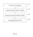
- FIG. 2 is an illustration of a flow chart of an example of a method for forming a patterned layer.
- Step 210 comprises forming a film of a photoresist on a substrate, where the photoresist composition may comprise a polymer, a PAG, and a PBG, such as described above.
- the concentration of the PAG may be higher than the concentration of the PBG.
- the polymer may have a structure comprising at least one acid labile group or at least one base soluble group.
- the PAG may be capable of generating a first amount of acid upon exposure to a first dose of radiation, and capable of generating a second amount of acid upon exposure to a second dose of radiation, where the second amount of acid is greater than the first amount of acid, and the second dose of radiation is greater than said first dose of radiation.
- the PBG generator may be capable of generating a first amount of base upon exposure to the same first dose of radiation (for example, the same magnitude and wavelength of radiation), and capable of generating a second amount of base upon exposure to the same second dose of radiation, where the first amount of base is greater than the first amount of acid (i.e. base is in excess of acid), and the second amount of base is less than the second amount of acid (i.e. the acid is in excess of base).
- the film may be formed by a process such as spin coating, spray coating, dip coating, doctor-blading, roll coating, and the like, which may be used individually or in one or more combination thereof in accordance with the methods of the present invention.
- the substrate may comprise materials of one or more of the IUPAC Groups 4, 6, 11, 12, 13, 14, and 15 elements, plastic material, silicon dioxide, glass, fused silica, mica, ceramic, metals deposited on the aforementioned substrates, combinations thereof, and the like.
- the substrate may comprise a stack or layering of different materials.
- a substrate used in a trilayer approach there may be a comparatively thick organic underlayer and a thin Si containing interlayer, where the Si containing layer may either be a chemical vapor deposited silicon oxide layer or a spin coated silsesquioxane polymer film.
- a substrate may comprise a prepared silicon wafer substrate such as those employed in semiconductor manufacturing. The films and layers described herein may be disposed on top of the substrate or may be integrally joined with the substrate.
- Step 215 comprises exposing a first region of the film to radiation having a first exposure dose, resulting in the photosensitive acid generator generating a first acid catalyst in the exposed first region of the film and the photosensitive base generator generating a first base in the exposed first region of the film, where the exposed first region comprises a first low dose region and a first high dose region.
- a high dose region comprises a portion of an exposed region receiving radiation of sufficiently high dosage such that the amount of acid generated by the PAG is greater than the amount of base generated by the PBG, such as the high radiation dose range 115 in FIG. 1 .
- a low dose region comprises a portion of an exposed region receiving radiation of sufficiently low dosage such that the amount of base generated by the PBG is greater than the amount of acid generated by the PAG, such as the low radiation dose range 110 in FIG. 1 .
- the concentration of the acid catalyst is higher than the concentration of the base (such as in high dose regions)
- the concentration of the acid catalyst is lower than the concentration of the base (such as in low dose regions).
- the film may comprise a plurality of exposed regions, each comprising a plurality of low dose regions and a plurality of high dose regions, where each low dose region is included in the plurality of low dose regions, and each high dose region is included in the plurality of high dose regions.
- the first base may be in sufficient excess of the first acid catalyst in the first low dose region such that a first portion of the first base neutralizes essentially all of the first acid catalyst in the first low dose region and a second portion of the first base remains in the first low dose region.
- the boundary areas between the first exposed region and unexposed regions of the film may be a low dose region, such as an exposed boundary area as described above, where the PBG generates an amount of base in excess of acid catalyst generated by the PAG, such as is illustrated in FIG. 1 .
- the first acid catalyst may be in sufficient excess of the first base in the first high dose region such that a first portion of the first acid neutralizes essentially all of the first base in the first high dose region and a second portion of the first acid catalyst remains in the first high dose region. For example, areas of the first exposed region near the center of the exposed area, away from boundary areas may be high dose regions.
- the remaining portion of the first acid catalyst may interact with the polymer of the photoresist, such as by crosslinking or acid catalyzed bond cleavage.
- Step 220 comprises exposing a second region of the film to radiation having a second exposure dose, resulting in the photosensitive acid generator generating a second acid catalyst in the exposed second region of the film and the photosensitive base generator generating a second base in the exposed second region of the film, where the exposed second region comprises a second low dose region and a second high dose region.
- the first exposure dose and the second exposure dose may be equal or different.
- the first exposure dose may be higher or lower than the first exposure dose depending on the formulation of the resist and the process steps applied before the second exposure.
- the second base may be in sufficient excess of the second acid catalyst in the second low dose region such that a first portion of the second base neutralizes essentially all of the second acid catalyst in the second low dose region and a second portion of the second base remains in the second low dose region.
- the boundary areas between the second exposed region and unexposed regions of the film may be a low dose region, such as an exposed boundary area as described above, where the PBG generates an amount of base in excess of acid catalyst generated by the PAG, such as is illustrated in FIG. 1 .
- the second acid catalyst may be in sufficient excess of the second base in the second high dose region such that a first portion of the second acid neutralizes essentially all of the second base in the second high dose region and a second portion of the second acid catalyst remains in the second high dose region.
- areas of the second exposed region near the center of the exposed area, away from boundary areas may be high dose regions.
- the remaining portion of the second acid in the high dose region may interact with the polymer of the photoresist, such as by crosslinking or acid catalyzed bond cleavage.
- Exposing the first region of the film to radiation in step 215 may comprise patternwise imaging the film through a first mask having a first image pattern.
- Exposing the second region of the first film to radiation in step 220 may comprise patternwise imaging the film through a second mask having a second image pattern.
- the first image pattern may be different or the same as the second image pattern.
- Resulting from patternwise imaging the film through the first mask and patternwise imaging the film through the second mask at least one area of the film may remain unexposed to the radiation and a second region of the film may be exposed to the radiation.
- the first and second image patterns may each have sections essentially transparent to the radiation, and each may have sections essentially opaque to the radiation.
- each image pattern may or may not coincide, such that after the first and second exposures, there may be areas of the film which remain unexposed to radiation. Likewise, there may be regions of the film which have been exposed through the first image pattern, the second image pattern, or both.
- the exposed regions of the film may comprise the first region exposed in steps 215 and the second region exposed in step 220 .
- one of the exposed first regions may be adjacent to or contiguous with one of the second exposed regions (e.g. the first exposed region and the second exposed region share an edge or boundary).
- Excess base in overlapping low dose areas prevents the first and second exposed regions from overlapping their acid distribution with each other, resulting in improving the resolution of the double exposed patterns from the two exposures, by neutralizing acid catalyst in the low dose areas between the two exposed regions and preventing the acid catalyst from reacting with the polymer of the photoresist.
- base proliferator in the resist formulation may enhance the base concentration in the boundary areas through base proliferation, such as through baking at elevated temperature. Therefore, a baking step may be used between step 215 and 220 when the resist composition further comprises a base proliferator.
- the resist film may be baked at a temperature between about 80° C. and about 150° C.
- the method may further comprise step 225 , step 225 comprising removing soluble portions of the film, after exposing the second region, to leave a patterned layer remaining, where the patterned layer has a photoresist pattern.
- removing soluble portions of the film may comprise developing the film in an aqueous base solution where the base-soluble exposed regions (or unexposed region for a negative tone resist) of the film may be removed from the film to form a patterned layer of the photoresist film.
- the developer may be organic or aqueous based, such as an aqueous base developer such as tetramethylammonium hydroxide (TMAH) aqueous solution, for example.
- TMAH tetramethylammonium hydroxide
- FIG. 3A is an illustration of a film 303 , comprising a photoresist, disposed on a substrate 300 , such as the photoresist films and substrates described above.
- FIG. 3B is an illustration of the film 303 of FIG. 3A being exposed to radiation as described for step 215 of FIG. 2 , wherein a first radiation source 310 projects radiation through a first patterned mask 315 onto the film 303 disposed on the substrate 300 .
- the first mask 315 may have a first image pattern comprising masked sections 320 , which are essentially opaque to the radiation, and unmasked sections 325 , which are essentially transparent to the radiation.
- Radiation passing through the unmasked sections 325 may be transmitted to the film 303 and simultaneously be received and absorbed in high dose region 330 and adjacent low dose regions 335 of the film 303 .
- the dose of radiation in the high dose region 330 may be in a range of high radiation dosage, such as the high radiation dose range 115 illustrated in FIG. 1 .
- the dose of radiation received by the low dose region 335 may be in a range of low radiation dosage, such as the low radiation dose range 110 of FIG. 1 .
- the film may comprise unexposed areas 305 after the first exposure to radiation.
- the radiation may induce the production of an acid catalyst by the PAG in the exposed regions 330 and 335 of the film 303 , where unexposed areas 305 of film 303 may not produce an acid catalyst.
- the radiation may induce the production of base by the PBG in the exposed regions 330 and 335 , where in low dose regions 335 the produced base may be in higher concentration than acid and may neutralize essentially all the acid catalyst produced in the low dose regions 335 .
- the acid catalyst produced by the PAG may be in higher concentration than the base produced by the PBG and thus the acid in the high dose region may neutralize essentially all of the base in the high dose region 330 .
- Sufficient acid catalyst may remain in the high dose regions 330 after reaction with the base to interact with the polymer of the photoresist, such as by crosslinking or acid catalyzed bond cleavage.
- FIG. 3C is an illustration of the exposed film 303 in FIG. 3B undergoing a second exposure, wherein a second radiation source 345 projects radiation through a second patterned mask 350 onto the film 303 disposed on a substrate 300 .
- the film may further comprise exposed regions 337 and 365 , where 365 may be a high dose region and adjacent region 337 may be a low dose region, such as is described above.
- At least one area 305 of the film 303 may remain unexposed after the first and second exposures.
- At least one low dose region 335 and at least one low dose region 337 may overlap to form an overlap area 339 between two adjacent exposed regions.
- the PAG may produce an acid catalyst in the high dose region 335 and the low dose region 337 , where the acid produced in the low dose region 337 by the PAG may be essentially neutralized by base produced in the low dose region 337 by the PBG as a result of the second exposure to radiation.
- Base produced by the PBG in the high dose region 365 may be essentially neutralized by a portion of the acid produced in sufficient excess in the high dose region 365 by the PAG such that a portion of the acid remains and may react with the polymer of the photoresist.
- the excess base produced in the overlap area 339 neutralizes acid catalyst in the overlap area 339 thus preventing interaction of the acid catalyst with the polymer of the photoresist in the overlap area 339 .
- the photoresist may comprise a negative tone photoresist, where the polymer may be configured such that, as a result of the first and second exposures, unexposed areas 305 , low dose regions 335 and 337 , and overlap region 339 may be removed in a developing step comprising developing the film 303 in a developer (such as aqueous base or solvent), where the unexposed areas 305 , low dose regions 335 and 337 , and overlap region 339 of the film 303 are base-soluble regions.
- a developer such as aqueous base or solvent
- Such a polymer configuration may comprise base-soluble groups in the polymer structure, where acid catalyst reaction with the polymer in the high dose regions 330 and 365 may render the polymer insoluble in aqueous base developer.
- the polymer in the high dose regions 330 and 365 may undergo crosslinking and become insoluble in developer.
- the photoresist may comprise a positive tone photoresists, where the polymer may be configured such that, as a result of the first and second exposures, exposed regions of the film 303 may be removed in a developing step comprising developing the film in a developer (such as aqueous base or solvent), where the exposed regions of the film are base-soluble, such as where acid catalyst reacts with the polymer (such as high dose regions 365 and 330 ).
- a developer such as aqueous base or solvent
- acid catalyst reacts with the polymer (such as high dose regions 365 and 330 ).
- Such a polymer configuration may comprise a polymer structure having acid labile groups which may be cleaved by reaction with the acid catalyst, thus rendering the polymer soluble in developer.
- the film may be baked at a temperature between about 80° C. and about 150° C.
- FIG. 3D is an illustration of the doubly exposed film 303 in FIG. 3C after the film has been developed in a developer (such as aqueous base) and, as a result of the developing, unexposed areas 305 and low dose regions 335 , 337 and 339 of the film 303 have been removed and a first patterned layer 380 of the film 303 is formed.
- the first patterned layer may have a photoresist pattern comprising features 370 and 375 remaining on the surface of the substrate 300 , where features 370 and 375 are formed from exposed high dose regions 365 and 330 , respectively.
- the polymer composition was such that the acid catalyst produced in the exposed areas 365 and 330 of FIG.
- FIG. 3E is an illustration of the doubly exposed film 303 in FIG. 3C after the film has been developed in a developer (such as aqueous base) and, as a result of the developing, exposed high dose regions 330 and 365 of the film 303 have been removed and a second patterned layer 395 of the film 303 is formed.
- the second patterned layer 395 may have a photoresist pattern comprising features 396 , 398 , and 397 remaining on the surface of the substrate 300 , as well as open gaps 385 and 390 where gaps 385 and 390 are open areas remaining after the removal of exposed high dose regions 330 and 365 , respectively.
- a developer such as aqueous base
- the polymer composition was such that the acid catalyst produced in the exposed high dose regions 365 and 330 of FIG. 3C interacted with the polymer in such a way as to render the polymer in those regions soluble in developer such that the exposed high dose regions 365 and 330 were removed, leaving unexposed areas 305 and low dose regions 335 , 337 and 339 to leave the patterned layer 395 remaining.
- the photoresist pattern of the patterned layer may be transferred to the substrate.
- the substrate comprises an antireflective coating (ARC) and/or planarizing underlayer onto which the photoresist film has been formed
- the ARC and/or planarizing underlayer may be removed at the gaps in the patterned photoresist layer to expose portions of the substrate.
- the antireflective coating and/or planarizing underlayer may be removed by etching.
- the photoresist pattern in the patterned layer (e.g. the pattern of gaps within the exposed film) may be transferred to portions of the substrate.
- Transferring the pattern may comprise, for example, etching, such as reactive ion etching (RIE), depositing (such as vapor deposition or electroplating) a material (such as a dielectric, a metal, a ceramic or a semiconductor) onto the substrate in a gap in the exposed photoresist film, by implanting dopants into the substrate material in a gap in the exposed photoresist film, or by a combination of one or more of these methods.
- etching such as reactive ion etching (RIE)
- depositing such as vapor deposition or electroplating
- a material such as a dielectric, a metal, a ceramic or a semiconductor
- the photoresists and films thereof described herein may be patternwise imaged using radiation such as ultraviolet (UV) such as wavelengths of approximately 436 nanometers (nm) and 365 nm, deep-ultraviolet (DUV) such as wavelengths of approximately 257 nm, 248 nm, 193 nm, and 157 nm, extreme-ultraviolet (EUV) such as a wavelength of approximately 4 nm to approximately 70 nm such as approximately 13 nm, x-ray, combinations of these, and the like.
- UV ultraviolet
- DUV deep-ultraviolet
- EUV extreme-ultraviolet
- Various wavelengths of radiation may be used such as 313 nm, 334 nm, 405 nm, and 126 nm etc., where the sources may be mainly from specific mercury emission lines or specific lasers.
- the sources may be mainly from specific mercury emission lines or specific lasers.
- single wavelength and/or narrow band radiation sources may be used.
- a broad band multiple wavelength source may be used.
- the photoresist compositions of the present invention may be patternwise imaged using particle beams such as electron beam, ion beam, combinations of these, and the like.
- the appropriate radiation or particle beam type(s) may depend on the components of the overall photoresist composition (e.g., the selection of the PBG, polymer, photosensitive acid generator (PAG), base proliferator, base (or quencher), surfactant, solvent, etc.).
- the selection of the PBG, polymer, photosensitive acid generator (PAG), base proliferator, base (or quencher), surfactant, solvent, etc. e.g., the selection of the PBG, polymer, photosensitive acid generator (PAG), base proliferator, base (or quencher), surfactant, solvent, etc.
- a terpolymer comprising 45 mole % MAdMA, 15 mole % STAR and 40 mole % NLM was dissolved in PGMEA with 4 wt % TPSN (triphenyl sulfonium nonaflate), 0.85 weight % (wt %) (i.e. 20 mole %) of DNC and 0.93 wt % (i.e. 20 mole %) of DFC (all wt. % are relative to total polymer weight) to make a solution having 7 wt % of solid content.
- the resulting solution was filtered through a 0.2 micron ( ⁇ m) filter.
- the resist was spin coated onto a 12 inch silicon wafer which had an approximately 42 nanometer (nm) thickness coating of Rohm & Haas bottom anti-reflective coating (BARC) named AR40A.
- the resist was post-applying baked (PAB) at about 110° C. for about 60 seconds and exposed to 193 nm wavelength light on an ASML stepper (1.1 NA, 0.75 outer and 0.55 inner ⁇ annular illumination).
- the wafer was then post-exposure baked (PEB) at about 120° C. for about 60 seconds.
- the film was developed using a single puddle develop process for about 30 seconds with 0.263 N TMAH (tetramethylammonium hydroxide) developer.
- TMAH tetramethylammonium hydroxide
- a terpolymer comprising 45 mole % MAdMA, 15 mole % STAR and 40 mole % NLM was dissolved in PGMEA with 4 wt % TPSN (triphenyl sulfonium nonaflate), 0.40 wt % (i.e. 20 mole %) of NBC-101 and 0.93 wt % (20 mole %) of DFC (all wt. % are relative to total polymer weight) to make a solution having 7 wt % of solid content.
- the resulting solution was filtered through a 0.2 ⁇ m filter.
- the resist was spin coated onto a 12 inch silicon wafer which had an approximately 42 nm thickness coating of Rohm & Haas bottom anti-reflective coating (BARC) named AR40A.
- the resist was post-applying baked (PAB) at about 110° C. for about 60 seconds and exposed to 193 nm wavelength light on an ASML stepper (1.1 NA, 0.75 outer and 0.55 inner ⁇ annular illumination).
- the wafer was then post-exposure baked (PEB) at about 120° C. for about 60 seconds.
- the film was then developed using a single puddle develop process for about 30 seconds with 0.263 N TMAH developer. At the dose of 14.8 mj/cm2, the 85 nm lines on a 180 nm pitch were resolved.
- a terpolymer comprising 45 mole % MAdMA, 15 mole % STAR and 40 mole % NLM was dissolved in PGMEA with 4 wt % TPSN (triphenyl sulfonium nonaflate), 0.14 wt % (i.e. 5 mole %) of ANC and 0.93 wt % (i.e. 20 mole %) of DFC (all wt. % are relative to total polymer weight) to make a solution with about 7 wt % of solid content.
- the resulting solution was filtered through a 0.2 ⁇ m filter.
- the resist was spin coated onto a 12 inch silicon wafer which had an approximate 42 nm thickness coating of Rohm & Haas bottom anti-reflective coating (BARC) named AR40A.
- the resist was post-applying baked (PAB) at about 110° C. for about 60 seconds and exposed to 193 nm wavelength light on an ASML stepper (1.1 NA, 0.75 outer and 0.55 inner 6 annular illumination).
- the wafer was then post-exposure baked (PEB) at about 120° C. for about 60 seconds.
- the film was developed using a single puddle develop process for about 30 seconds with 0.263 N TMAH developer. At the dose of 14.8 mj/cm2, 85 nm lines on a 180 nm pitch were resolved.
Abstract
Description


where R1═H or alkyl group, R2=alkyl, substituted alkyl, aryl or substituted aryl group, R3, R4═H, alkyl, substituted alkyl, aryl or substituted aryl group, and R5=aryl group, R1 and R2 may link to form a cyclic structure, such as 2-nitrobenzyl carbamates where R5 is a 2-nitrophenyl group and R3, R4═H;
Carbamates of the Structure
where R1═H or alkyl group, R2=alkyl, substituted alkyl, aryl or substituted aryl group, R1 and R2 may link to form a cyclic structure, and R3=alkyl, substituted alkyl, aryl or substituted aryl group;
Benzoin Carbamates (2-Oxo-1,2-Diphenyithyl Carbamates) of the Structure

where R1═H or alkyl group, R2=alkyl, substituted alkyl, aryl or substituted aryl group, R1 and R2 may link to form a cyclic structure, and R5 and R6 may each independently be an aryl or a substituted aryl group, such as benzoin carbamates where R1═H, R2═C6 to C10 alkyl group, and R5 and R6 are each phenyl groups;
O-Carbamoylhydroxylamines of the Structure

where R1═H or alkyl group; R2=alkyl, substituted alkyl, aryl or substituted aryl group, R1 and R2 may link to form a cyclic structure, and R3, R4═H, alkyl, substituted alkyl, aryl, substituted aryl, or acyl group, such as O-carbamolhydroxphthalamides where R1═H, R2═C6 to C10 alkyl group, and R3 and R4 are each a 2-carboxybenzoyl group;
O-Carbamoyloximes of the Structure

where R1═H or alkyl group, R2=alkyl or aryl group, and R3, R4═H, alkyl, substituted alkyl, aryl, or substituted aryl group;
Aromatic Sulfonamides of the Structure

where R1═H or alkyl group, R2=alkyl, substituted alkyl, aryl or substituted aryl group, R1 and R2 may link to form a cyclic structure, and R3=aryl group or substituted aryl groups;
α-Lactones of the Structure

where R2=alkyl, aryl group, R3=alkyl, substituted alkyl, aryl, or substituted aryl group;
N-(2-Arylethenyl)amides of the structure

where R3=alkyl, substituted alkyl, aryl, or substituted aryl group, R4=alkyl or substituted alkyl group, and R5=aryl group;
Azides of the Structure
R6N3
where R6=aryl or substituted aryl group;
Amides of the Structure
where R6=aryl or substituted aryl group, R7═H, alkyl, substituted alkyl, aryl or substituted aryl group;
Oximines of the Structure

where R3, R4, R8=alkyl, substituted alkyl, aryl or substituted aryl group;
Quaternary Ammonium Salts of the Structure

where R3, R4, R8, R9=alkyl, substituted alkyl, aryl or substituted aryl group, A−=an anion such as a halide ion (such as Cl−, BR−, I−, F−, etc.) or sulfonate ion; and
Amineimides of the Structure

Where each of R3, R4, R8 and R9 is an alkyl, substituted alkyl, aryl or substituted aryl group, In all the above structural formulas: R1 is H, an alkyl group or a substituted alkyl group; and R2 is an alkyl group, substituted alkyl group, an aromatic group, or an substituted aromatic group. The PBG described above may also be linked to form dimers, where such a linkage may prevent volatility of the base produced.


wherein each R1 or R2 is independently selected from the group consisting of a hydrogen atom, a linear alkyl, a branched alkyl, a cycloalkyl, a halogenated linear alkyl, a halogenated branched alkyl, a halogenated cycloalkyl, an aryl, a halogenated aryl, and combinations thereof, and wherein R4 may be hydrogen or alkyl. Halogenated may comprise fluorinated, chlorinated, or brominated. For example, each R1 or R2 may be independently selected from the group consisting of a fluorinated linear alkyl, a fluorinated branched alkyl, a fluorinated cycloalkyl, an aryl, a fluorinated aryl, and combinations thereof, wherein R3 is selected from the group consisting of a fluorinated linear alkyl, a fluorinated branched alkyl, a fluorinated cycloalkyl, an aryl, a fluorinated aryl, and combinations thereof.

wherein each R1 or R2 is independently selected from the group consisting of a hydrogen atom, a linear alkyl, a branched alkyl, a cycloalkyl, a halogenated linear alkyl, a halogenated branched alkyl, a halogenated cycloalkyl, an aryl, a halogenated aryl, and combinations thereof, wherein R3 is selected from the group consisting of a linear alkyl, a branched alkyl, a cycloalkyl, a halogenated linear alkyl, a halogenated branched alkyl, a halogenated cycloalkyl, an aryl, a halogenated aryl, and combinations thereof, and wherein R4 may be hydrogen or alkyl. As above, halogenated may comprise fluorinated, chlorinated, or brominated. For example, each R1 or R2 may be independently selected from the group consisting of a fluorinated linear alkyl, a fluorinated branched alkyl, a fluorinated cycloalkyl, an aryl, a fluorinated aryl, and combinations thereof, wherein R3 is selected from the group consisting of a fluorinated linear alkyl, a fluorinated branched alkyl, a fluorinated cycloalkyl, an aryl, a fluorinated aryl, and combinations thereof.
Claims (19)


Priority Applications (1)
| Application Number | Priority Date | Filing Date | Title |
|---|---|---|---|
| US14/457,149 US9235119B2 (en) | 2008-01-08 | 2014-08-12 | Exposure photolithography methods |
Applications Claiming Priority (3)
| Application Number | Priority Date | Filing Date | Title |
|---|---|---|---|
| US11/970,761 US8236476B2 (en) | 2008-01-08 | 2008-01-08 | Multiple exposure photolithography methods and photoresist compositions |
| US13/461,960 US8846296B2 (en) | 2008-01-08 | 2012-05-02 | Photoresist compositions |
| US14/457,149 US9235119B2 (en) | 2008-01-08 | 2014-08-12 | Exposure photolithography methods |
Related Parent Applications (1)
| Application Number | Title | Priority Date | Filing Date |
|---|---|---|---|
| US13/461,960 Continuation US8846296B2 (en) | 2008-01-08 | 2012-05-02 | Photoresist compositions |
Publications (2)
| Publication Number | Publication Date |
|---|---|
| US20140349237A1 US20140349237A1 (en) | 2014-11-27 |
| US9235119B2 true US9235119B2 (en) | 2016-01-12 |
Family
ID=40404361
Family Applications (4)
| Application Number | Title | Priority Date | Filing Date |
|---|---|---|---|
| US11/970,761 Expired - Fee Related US8236476B2 (en) | 2008-01-08 | 2008-01-08 | Multiple exposure photolithography methods and photoresist compositions |
| US13/418,421 Active US8568960B2 (en) | 2008-01-08 | 2012-03-13 | Multiple exposure photolithography methods |
| US13/461,960 Expired - Fee Related US8846296B2 (en) | 2008-01-08 | 2012-05-02 | Photoresist compositions |
| US14/457,149 Expired - Fee Related US9235119B2 (en) | 2008-01-08 | 2014-08-12 | Exposure photolithography methods |
Family Applications Before (3)
| Application Number | Title | Priority Date | Filing Date |
|---|---|---|---|
| US11/970,761 Expired - Fee Related US8236476B2 (en) | 2008-01-08 | 2008-01-08 | Multiple exposure photolithography methods and photoresist compositions |
| US13/418,421 Active US8568960B2 (en) | 2008-01-08 | 2012-03-13 | Multiple exposure photolithography methods |
| US13/461,960 Expired - Fee Related US8846296B2 (en) | 2008-01-08 | 2012-05-02 | Photoresist compositions |
Country Status (5)
| Country | Link |
|---|---|
| US (4) | US8236476B2 (en) |
| EP (1) | EP2240828B1 (en) |
| KR (1) | KR20100102189A (en) |
| TW (1) | TWI472873B (en) |
| WO (1) | WO2009087029A1 (en) |
Families Citing this family (24)
| Publication number | Priority date | Publication date | Assignee | Title |
|---|---|---|---|---|
| US8236476B2 (en) | 2008-01-08 | 2012-08-07 | International Business Machines Corporation | Multiple exposure photolithography methods and photoresist compositions |
| JP5573578B2 (en) * | 2009-10-16 | 2014-08-20 | 信越化学工業株式会社 | Pattern forming method and resist material |
| JP5621735B2 (en) * | 2010-09-03 | 2014-11-12 | 信越化学工業株式会社 | Pattern forming method and chemically amplified positive resist material |
| WO2012060827A1 (en) * | 2010-11-03 | 2012-05-10 | Empire Technology Development Llc | Lithography using photoresist with photoinitiator and photoinhibitor |
| US9599895B2 (en) | 2011-04-12 | 2017-03-21 | Empire Technology Development Llc | Lithography using photoresist with photoinitiator and photoinhibitor |
| KR20130039124A (en) | 2011-10-11 | 2013-04-19 | 삼성전자주식회사 | Method for forming patterns of semiconductor device |
| WO2013137157A1 (en) * | 2012-03-14 | 2013-09-19 | Jsr株式会社 | Photoresist composition, method for forming resist pattern, acid diffusion control agent and compound |
| US8741551B2 (en) * | 2012-04-09 | 2014-06-03 | Taiwan Semiconductor Manufacturing Company, Ltd. | Method and composition of a dual sensitive resist |
| US8846295B2 (en) | 2012-04-27 | 2014-09-30 | International Business Machines Corporation | Photoresist composition containing a protected hydroxyl group for negative development and pattern forming method using thereof |
| US9304396B2 (en) | 2013-02-25 | 2016-04-05 | Lam Research Corporation | PECVD films for EUV lithography |
| US9772558B2 (en) | 2013-09-24 | 2017-09-26 | International Business Machines Corporation | Sulfonic acid ester containing polymers for organic solvent based dual-tone photoresists |
| US9320387B2 (en) | 2013-09-30 | 2016-04-26 | Lam Research Corporation | Sulfur doped carbon hard masks |
| US9589799B2 (en) | 2013-09-30 | 2017-03-07 | Lam Research Corporation | High selectivity and low stress carbon hardmask by pulsed low frequency RF power |
| US9645391B2 (en) | 2013-11-27 | 2017-05-09 | Tokyo Electron Limited | Substrate tuning system and method using optical projection |
| KR101888287B1 (en) * | 2014-01-27 | 2018-08-13 | 도쿄엘렉트론가부시키가이샤 | System and method for shifting critical dimensions of patterned films |
| JP6895600B2 (en) * | 2014-02-25 | 2021-06-30 | 東京エレクトロン株式会社 | Chemical Amplification Methods and Techniques for Developable Bottom Anti-Reflective Coatings and Colored Implant Resists |
| WO2016025210A1 (en) * | 2014-08-13 | 2016-02-18 | Tokyo Electron Limited | Critical dimension control in photo-sensitized chemically-amplified resist |
| JP2016071243A (en) * | 2014-09-30 | 2016-05-09 | 富士フイルム株式会社 | Method for forming resin pattern, method for forming pattern, cured film, liquid crystal display device, organic el display device, and touch panel display device |
| JP6606926B2 (en) * | 2015-08-27 | 2019-11-20 | Jsr株式会社 | Radiation-sensitive resin composition, resist pattern forming method and compound |
| US10095112B2 (en) * | 2017-02-24 | 2018-10-09 | Irresistible Materials Ltd | Multiple trigger photoresist compositions and methods |
| KR102602567B1 (en) | 2018-02-26 | 2023-11-14 | 닛뽄 가야쿠 가부시키가이샤 | Base propagating agent and base-reactive resin composition containing the base propagating agent |
| WO2019183056A1 (en) * | 2018-03-19 | 2019-09-26 | Tokyo Electron Limited | Method for correcting critical dimensions using calibrated trim dosing |
| WO2020243342A1 (en) | 2019-05-29 | 2020-12-03 | Lam Research Corporation | High selectivity, low stress, and low hydrogen diamond-like carbon hardmasks by high power pulsed low frequency rf |
| US20220373897A1 (en) * | 2019-11-19 | 2022-11-24 | Applied Materials, Inc. | Lithography apparatus, patterning system, and method of patterning a layered structure |
Citations (40)
| Publication number | Priority date | Publication date | Assignee | Title |
|---|---|---|---|---|
| EP0425142A2 (en) | 1989-10-27 | 1991-05-02 | Rohm And Haas Company | Positive acting photoresist and method of producing same |
| US5576143A (en) | 1991-12-03 | 1996-11-19 | Fuji Photo Film Co., Ltd. | Light-sensitive composition |
| JPH1083079A (en) | 1996-09-06 | 1998-03-31 | Shin Etsu Chem Co Ltd | Chemical amplification positive type resist material |
| US5837426A (en) | 1996-07-29 | 1998-11-17 | United Microelectronics Corp. | Photolithographic process for mask programming of read-only memory devices |
| JP2000010270A (en) | 1998-04-23 | 2000-01-14 | Sumitomo Chem Co Ltd | Chemical amplification type positive type photoresist composition |
| JP2000330270A (en) | 1999-05-24 | 2000-11-30 | Kunihiro Ichimura | Base propagator, base propagator composition, reactive base composition and pattern forming method |
| US6219786B1 (en) | 1998-09-09 | 2001-04-17 | Surfcontrol, Inc. | Method and system for monitoring and controlling network access |
| US6319649B1 (en) | 1994-10-13 | 2001-11-20 | Hitachi, Ltd. | Photosensitive resin composition and method of forming resist images |
| US6338934B1 (en) | 1999-08-26 | 2002-01-15 | International Business Machines Corporation | Hybrid resist based on photo acid/photo base blending |
| WO2002034714A1 (en) | 2000-10-24 | 2002-05-02 | Toda Kogyo Corporation | Base-proliferating prepolymers |
| US6395451B1 (en) | 1999-09-21 | 2002-05-28 | Hyundai Electronics Industries Co., Ltd. | Photoresist composition containing photo base generator with photo acid generator |
| US20020110762A1 (en) | 2001-02-09 | 2002-08-15 | United Microelectronics Corp. | Photolithographic process |
| JP2002265531A (en) | 2001-03-13 | 2002-09-18 | Kunihiro Ichimura | Base-proliferating unsaturated compound, base- proliferating resin, and composition containing the resin |
| US20020160317A1 (en) | 2001-04-27 | 2002-10-31 | Richter Ernst-Christian | Method for structuring a photoresist layer |
| US6645693B2 (en) | 2000-06-30 | 2003-11-11 | Sumitomo Chemical Company, Limited | Resist composition |
| US6692897B2 (en) | 2000-07-12 | 2004-02-17 | Fuji Photo Film Co., Ltd. | Positive resist composition |
| JP2004077553A (en) | 2002-08-09 | 2004-03-11 | Hitachi Chemical Dupont Microsystems Ltd | Photosensitive resin composition and method for manufacturing relief pattern, heat-resistant coating film and heat-resistant insulating pattern by using the same, and electronic parts having them |
| JP2004099579A (en) | 2002-09-09 | 2004-04-02 | Kunihiro Ichimura | Base-proliferative silicon compound, base proliferative siloxane resin and photosensitive resin composition |
| US20040133640A1 (en) | 2002-10-31 | 2004-07-08 | Yeager William J. | Presence detection using mobile agents in peer-to-peer networks |
| US6794110B2 (en) | 2002-03-04 | 2004-09-21 | International Business Machines Corporation | Polymer blend and associated methods of preparation and use |
| US6800414B2 (en) | 2000-06-16 | 2004-10-05 | Jsr Corporation | Radiation-sensitive resin composition |
| US6969577B2 (en) | 2003-03-04 | 2005-11-29 | Fuji Photo Film Co., Ltd. | Positive resist composition |
| US20050271981A1 (en) | 2004-05-31 | 2005-12-08 | Hidekazu Oohashi | Method for colored image formation |
| US20060065122A1 (en) | 2004-09-30 | 2006-03-30 | Wei-Liang Song | Gas chromatograph system including an improved inlet sealing mechanism |
| US20060088792A1 (en) * | 2004-10-27 | 2006-04-27 | Renesas Technology Corp. | Pattern forming method, semiconductor device manufacturing method and exposure mask set |
| US20060125847A1 (en) | 2004-12-14 | 2006-06-15 | International Business Machines Corporation | Automated display of an information technology system configuration |
| WO2006095670A1 (en) | 2005-03-11 | 2006-09-14 | Sekisui Chemical Co., Ltd. | Base multiplying agents and base-reactive curable compositions |
| US7157208B2 (en) | 2004-02-20 | 2007-01-02 | Fuji Photo Film Co., Ltd. | Positive resist composition and pattern forming method using the same |
| US20070014233A1 (en) | 2005-02-10 | 2007-01-18 | Fujitsu Limited | Fault management apparatus and method for identifying cause of fault in communication network |
| US20070205528A1 (en) | 2004-03-22 | 2007-09-06 | Huntsman Advanced Materials Americans Inc. | Photocurable Compositions |
| US20080038662A1 (en) | 2006-08-10 | 2008-02-14 | Shin-Etsu Chemical Co., Ltd. | Bottom resist layer composition and patterning process using the same |
| US20080148378A1 (en) | 2006-10-13 | 2008-06-19 | Cisco Technology, Inc. | Discovering security devices located on a call path and extending bindings at those discovered security devices |
| US20080153030A1 (en) | 2006-12-25 | 2008-06-26 | Shin-Etsu Chemical Co., Ltd. | Positive resist composition and patterning process |
| US20090155718A1 (en) | 2007-12-13 | 2009-06-18 | International Business Machines Corporation | Photoresist compositions and method for multiple exposures with multiple layer resist systems |
| US20090176174A1 (en) | 2008-01-08 | 2009-07-09 | International Business Machines Corporation | Multiple exposure photolithography methods and photoresist compostions |
| US20100174731A1 (en) | 2005-12-29 | 2010-07-08 | Vermeulen Allan H | Distributed Storage System With Web Services Client Interface |
| US7838200B2 (en) | 2007-12-13 | 2010-11-23 | International Business Machines Corporation | Photoresist compositions and method for multiple exposures with multiple layer resist systems |
| US20120280061A1 (en) | 2010-02-01 | 2012-11-08 | Thermo Fisher Scientific S.P.A. | Vaporisation injector |
| US8383316B2 (en) | 2006-07-10 | 2013-02-26 | Pixelligent Technologies, Llc | Resists for lithography |
| US20130246606A1 (en) | 2012-03-13 | 2013-09-19 | International Business Machines Corporation | Detecting Transparent Network Communication Interception Appliances |
Family Cites Families (1)
| Publication number | Priority date | Publication date | Assignee | Title |
|---|---|---|---|---|
| TW200306324A (en) * | 2002-04-22 | 2003-11-16 | Tokyo Ind Co Ltd | Novolak resin solution, positive photoresist composition, and method of producing same |
-
2008
- 2008-01-08 US US11/970,761 patent/US8236476B2/en not_active Expired - Fee Related
- 2008-12-17 KR KR1020107016878A patent/KR20100102189A/en not_active Application Discontinuation
- 2008-12-17 WO PCT/EP2008/067736 patent/WO2009087029A1/en active Application Filing
- 2008-12-17 EP EP08869857.6A patent/EP2240828B1/en not_active Not-in-force
-
2009
- 2009-01-05 TW TW98100118A patent/TWI472873B/en not_active IP Right Cessation
-
2012
- 2012-03-13 US US13/418,421 patent/US8568960B2/en active Active
- 2012-05-02 US US13/461,960 patent/US8846296B2/en not_active Expired - Fee Related
-
2014
- 2014-08-12 US US14/457,149 patent/US9235119B2/en not_active Expired - Fee Related
Patent Citations (47)
| Publication number | Priority date | Publication date | Assignee | Title |
|---|---|---|---|---|
| US5650261A (en) | 1989-10-27 | 1997-07-22 | Rohm And Haas Company | Positive acting photoresist comprising a photoacid, a photobase and a film forming acid-hardening resin system |
| EP0425142A2 (en) | 1989-10-27 | 1991-05-02 | Rohm And Haas Company | Positive acting photoresist and method of producing same |
| US5576143A (en) | 1991-12-03 | 1996-11-19 | Fuji Photo Film Co., Ltd. | Light-sensitive composition |
| US6319649B1 (en) | 1994-10-13 | 2001-11-20 | Hitachi, Ltd. | Photosensitive resin composition and method of forming resist images |
| US5837426A (en) | 1996-07-29 | 1998-11-17 | United Microelectronics Corp. | Photolithographic process for mask programming of read-only memory devices |
| JPH1083079A (en) | 1996-09-06 | 1998-03-31 | Shin Etsu Chem Co Ltd | Chemical amplification positive type resist material |
| JP2000010270A (en) | 1998-04-23 | 2000-01-14 | Sumitomo Chem Co Ltd | Chemical amplification type positive type photoresist composition |
| US6219786B1 (en) | 1998-09-09 | 2001-04-17 | Surfcontrol, Inc. | Method and system for monitoring and controlling network access |
| JP2000330270A (en) | 1999-05-24 | 2000-11-30 | Kunihiro Ichimura | Base propagator, base propagator composition, reactive base composition and pattern forming method |
| US6338934B1 (en) | 1999-08-26 | 2002-01-15 | International Business Machines Corporation | Hybrid resist based on photo acid/photo base blending |
| US6395451B1 (en) | 1999-09-21 | 2002-05-28 | Hyundai Electronics Industries Co., Ltd. | Photoresist composition containing photo base generator with photo acid generator |
| US6800414B2 (en) | 2000-06-16 | 2004-10-05 | Jsr Corporation | Radiation-sensitive resin composition |
| US6645693B2 (en) | 2000-06-30 | 2003-11-11 | Sumitomo Chemical Company, Limited | Resist composition |
| US6692897B2 (en) | 2000-07-12 | 2004-02-17 | Fuji Photo Film Co., Ltd. | Positive resist composition |
| JP2002128750A (en) | 2000-10-24 | 2002-05-09 | Kunihiro Ichimura | Base proliferating prepolymer |
| WO2002034714A1 (en) | 2000-10-24 | 2002-05-02 | Toda Kogyo Corporation | Base-proliferating prepolymers |
| US20020110762A1 (en) | 2001-02-09 | 2002-08-15 | United Microelectronics Corp. | Photolithographic process |
| JP2002265531A (en) | 2001-03-13 | 2002-09-18 | Kunihiro Ichimura | Base-proliferating unsaturated compound, base- proliferating resin, and composition containing the resin |
| US20020160317A1 (en) | 2001-04-27 | 2002-10-31 | Richter Ernst-Christian | Method for structuring a photoresist layer |
| US6794110B2 (en) | 2002-03-04 | 2004-09-21 | International Business Machines Corporation | Polymer blend and associated methods of preparation and use |
| JP2004077553A (en) | 2002-08-09 | 2004-03-11 | Hitachi Chemical Dupont Microsystems Ltd | Photosensitive resin composition and method for manufacturing relief pattern, heat-resistant coating film and heat-resistant insulating pattern by using the same, and electronic parts having them |
| JP2004099579A (en) | 2002-09-09 | 2004-04-02 | Kunihiro Ichimura | Base-proliferative silicon compound, base proliferative siloxane resin and photosensitive resin composition |
| US20040133640A1 (en) | 2002-10-31 | 2004-07-08 | Yeager William J. | Presence detection using mobile agents in peer-to-peer networks |
| US6969577B2 (en) | 2003-03-04 | 2005-11-29 | Fuji Photo Film Co., Ltd. | Positive resist composition |
| US7157208B2 (en) | 2004-02-20 | 2007-01-02 | Fuji Photo Film Co., Ltd. | Positive resist composition and pattern forming method using the same |
| US20070205528A1 (en) | 2004-03-22 | 2007-09-06 | Huntsman Advanced Materials Americans Inc. | Photocurable Compositions |
| US20050271981A1 (en) | 2004-05-31 | 2005-12-08 | Hidekazu Oohashi | Method for colored image formation |
| US20060065122A1 (en) | 2004-09-30 | 2006-03-30 | Wei-Liang Song | Gas chromatograph system including an improved inlet sealing mechanism |
| US20060088792A1 (en) * | 2004-10-27 | 2006-04-27 | Renesas Technology Corp. | Pattern forming method, semiconductor device manufacturing method and exposure mask set |
| US20060125847A1 (en) | 2004-12-14 | 2006-06-15 | International Business Machines Corporation | Automated display of an information technology system configuration |
| US20070014233A1 (en) | 2005-02-10 | 2007-01-18 | Fujitsu Limited | Fault management apparatus and method for identifying cause of fault in communication network |
| WO2006095670A1 (en) | 2005-03-11 | 2006-09-14 | Sekisui Chemical Co., Ltd. | Base multiplying agents and base-reactive curable compositions |
| US20100174731A1 (en) | 2005-12-29 | 2010-07-08 | Vermeulen Allan H | Distributed Storage System With Web Services Client Interface |
| US8383316B2 (en) | 2006-07-10 | 2013-02-26 | Pixelligent Technologies, Llc | Resists for lithography |
| US20080038662A1 (en) | 2006-08-10 | 2008-02-14 | Shin-Etsu Chemical Co., Ltd. | Bottom resist layer composition and patterning process using the same |
| US20080148378A1 (en) | 2006-10-13 | 2008-06-19 | Cisco Technology, Inc. | Discovering security devices located on a call path and extending bindings at those discovered security devices |
| US20080153030A1 (en) | 2006-12-25 | 2008-06-26 | Shin-Etsu Chemical Co., Ltd. | Positive resist composition and patterning process |
| US20090155718A1 (en) | 2007-12-13 | 2009-06-18 | International Business Machines Corporation | Photoresist compositions and method for multiple exposures with multiple layer resist systems |
| US7838198B2 (en) | 2007-12-13 | 2010-11-23 | International Business Machines Corporation | Photoresist compositions and method for multiple exposures with multiple layer resist systems |
| US7838200B2 (en) | 2007-12-13 | 2010-11-23 | International Business Machines Corporation | Photoresist compositions and method for multiple exposures with multiple layer resist systems |
| US20090176174A1 (en) | 2008-01-08 | 2009-07-09 | International Business Machines Corporation | Multiple exposure photolithography methods and photoresist compostions |
| US8236476B2 (en) | 2008-01-08 | 2012-08-07 | International Business Machines Corporation | Multiple exposure photolithography methods and photoresist compositions |
| US20120178027A1 (en) | 2008-01-08 | 2012-07-12 | International Business Machines Corporation | Multiple exposure photolithography methods |
| US8568960B2 (en) | 2008-01-08 | 2013-10-29 | International Business Machines Corporation | Multiple exposure photolithography methods |
| US8846296B2 (en) | 2008-01-08 | 2014-09-30 | International Business Machines Corporation | Photoresist compositions |
| US20120280061A1 (en) | 2010-02-01 | 2012-11-08 | Thermo Fisher Scientific S.P.A. | Vaporisation injector |
| US20130246606A1 (en) | 2012-03-13 | 2013-09-19 | International Business Machines Corporation | Detecting Transparent Network Communication Interception Appliances |
Non-Patent Citations (29)
| Title |
|---|
| 312 amendment (Jun. 22, 2012) for U.S. Appl. No. 11/970,761, filed Jan. 8, 2008; Art Unit 1722; Confirmation No. 3670. |
| Advisory Action (mail date Aug. 21, 2013) for U.S. Appl. No. 13/461,960, filed May 2, 2012; Art Unit 1722; Confirmation No. 1010. |
| Amendment (Jan. 29, 2014) for U.S. Appl. No. 13/461,960, filed May 2, 2012; Art Unit 1722; Confirmation No. 1010. |
| Amendment (May 13, 2013) for U.S. Appl. No. 13/461,960, filed May 2, 2012; Art Unit 1722; Confirmation No. 1010. |
| Amendment filed Apr. 5, 2011 in response to Office Action (Mail Date Jan. 11, 2011) for U.S. Appl. No. 11/970,761, filed Jan. 8, 2008; Art Unit 1722; Confirmation No. 3670. |
| Amendment filed Jan. 27, 2012 in response to Office Action (Mail Date Oct. 28, 2011) for U.S. Appl. No. 11/970,761, filed Jan. 8, 2008; Art Unit 1722; Confirmation No. 3670. |
| Arimitsu et al.; Synthesis of 9-Fluorenylmethyl Carbamates as a Base Amplifier and Their Applications to Photopolymer Systems, Journal of Photopolymer Science and Technology, vol. 12, No. 2, (1999), pp. 317-318. |
| Arimitsu, et al.; Non-linear organic reaction of 9-fluorenylmethyl carbamates as base amplifiers to proliferate alphatic amines and their application to a novel photopolymer system, Journal of Materials Chemistry, 2004, 14, 336-343. |
| Final Amendment (Apr. 23, 2014) for U.S. Appl. No. 13/461,960, filed May 2, 2012; Art Unit 1722; Confirmation No. 1010. |
| Final Amendment (Aug. 14, 2013) for U.S. Appl. No. 13/461,960, filed May 2, 2012; Art Unit 1722; Confirmation No. 1010. |
| Final Office Action (mail date Feb. 21, 2014) for U.S. Appl. No. 13/461,960, filed May 2, 2012; Art Unit 1722; Confirmation No. 1010. |
| Final Office Action (Mail Date Jun. 13, 2011) for U.S. Appl. No. 11/970,761, filed Jan. 8, 2008; Art Unit 1722; Confirmation No. 3670. |
| Final Office Action (mail date Jun. 18, 2013) for U.S. Appl. No. 13/461,960, filed May 2, 2012; Art Unit 1722; Confirmation No. 1010. |
| Final Office Action (Mail Date Mar. 1, 2012) for U.S. Appl. No. 11/970,761, filed Jan. 8, 2008; Art Unit 1722; Confirmation No. 3670. |
| Glodde et al.; Measurements of Acid Generation by EUV Irradiation in Lithographic Films, Published in J. Vac. Sci. Technol. B., pp. 2496-2503, 25 () Nov. 2007, 13 pages. |
| Lee et al.; Photolithographic Micropatterning of an Electroluminescent Polymer Using Photobase Generator; Macromolecules 2003, vol. 36, No. 24; pp. 9252. |
| Machine translation of JP10083079, published on Mar. 31, 1998. |
| Machine translation of JP2004077553, published on Mar. 11, 2004. |
| Notice of Allowance (Mail Date May 15, 2012) for U.S. Appl. No. 11/970,761, filed Jan. 8, 2008; Art Unit 1722; Confirmation No. 3670. |
| Notice of Allowance (mail date May 7, 2014) for U.S. Appl. No. 13/461,960, filed May 2, 2012; Art Unit 1722; Confirmation No. 1010. |
| Office Action (Mail Date Apr. 25, 2012) for U.S. Appl. No. 11/970,761, filed Jan. 8, 2008; Art Unit 1722; Confirmation No. 3670. |
| Office Action (Mail Date Jan. 11, 2011) for U.S. Appl. No. 11/970,761, filed Jan. 8, 2008; Art Unit 1722; Confirmation No. 3670. |
| Office Action (mail date Jan. 11, 2013) for U.S. Appl. No. 13/461,960, filed May 2, 2012; Art Unit 1722; Confirmation No. 1010. |
| Office Action (mail date Mar. 21, 2013) for U.S. Appl. No. 13/418,421, filed Mar. 13, 2012; Art Unit 1722; Confirmation No. 8331. |
| Office Action (Mail Date Oct. 28, 2011) for U.S. Appl. No. 11/970,761, filed Jan. 8, 2008; Art Unit 1722; Confirmation No. 3670. |
| Office Action (mail date Oct. 31, 2013) for U.S. Appl. No. 13/461,960, filed May 2, 2012; Art Unit 1722; Confirmation No. 1010. |
| RCE (Sep. 18, 2013) for U.S. Appl. No. 13/461,960, filed May 2, 2012; Art Unit 1722; Confimration No. 1010. |
| Request for Continued Examination and Amendment filed Sep. 12, 2011 in response to Final Office Action (Mail Date Jun. 13, 2011) for U.S. Appl. No. 11/970,761, filed Jan. 8, 2008; Art Unit 1722; Confirmation No. 3670. |
| U.S. Appl. No. 13/418,421, filed Mar. 13, 2012; Art Unit 1722; Confirmation No. 8331. |
Also Published As
| Publication number | Publication date |
|---|---|
| EP2240828A1 (en) | 2010-10-20 |
| US20140349237A1 (en) | 2014-11-27 |
| US20120178027A1 (en) | 2012-07-12 |
| WO2009087029A1 (en) | 2009-07-16 |
| TW200947117A (en) | 2009-11-16 |
| US8236476B2 (en) | 2012-08-07 |
| TWI472873B (en) | 2015-02-11 |
| US20120214099A1 (en) | 2012-08-23 |
| US8846296B2 (en) | 2014-09-30 |
| EP2240828B1 (en) | 2015-11-25 |
| US8568960B2 (en) | 2013-10-29 |
| US20090176174A1 (en) | 2009-07-09 |
| KR20100102189A (en) | 2010-09-20 |
Similar Documents
| Publication | Publication Date | Title |
|---|---|---|
| US9235119B2 (en) | Exposure photolithography methods | |
| US7838198B2 (en) | Photoresist compositions and method for multiple exposures with multiple layer resist systems | |
| KR101967189B1 (en) | Substrate comprising self-aligned spacers | |
| US7838200B2 (en) | Photoresist compositions and method for multiple exposures with multiple layer resist systems | |
| KR101671289B1 (en) | Methods of forming electronic devices | |
| KR101746017B1 (en) | Methods of forming electronic devices | |
| US8846295B2 (en) | Photoresist composition containing a protected hydroxyl group for negative development and pattern forming method using thereof | |
| US8053172B2 (en) | Photoresists and methods for optical proximity correction | |
| US20050106494A1 (en) | Silicon-containing resist systems with cyclic ketal protecting groups | |
| US8021828B2 (en) | Photoresist compositions and methods related to near field masks | |
| US8932796B2 (en) | Hybrid photoresist composition and pattern forming method using thereof | |
| JP2712700B2 (en) | Pattern formation method | |
| TWI736549B (en) | Resist pattern forming method and developer for lithography | |
| US7566527B2 (en) | Fused aromatic structures and methods for photolithographic applications | |
| US6177229B1 (en) | Photosensitive composition |
Legal Events
| Date | Code | Title | Description |
|---|---|---|---|
| AS | Assignment |
Owner name: INTERNATIONAL BUSINESS MACHINES CORPORATION, NEW Y Free format text: ASSIGNMENT OF ASSIGNORS INTEREST;ASSIGNORS:CHEN, KUANG-JUNG;HUANG, WU-SONG;KWONG, RANEE WAI-LING;AND OTHERS;SIGNING DATES FROM 20140718 TO 20140805;REEL/FRAME:033511/0452 |
|
| FEPP | Fee payment procedure |
Free format text: PAYOR NUMBER ASSIGNED (ORIGINAL EVENT CODE: ASPN); ENTITY STATUS OF PATENT OWNER: LARGE ENTITY |
|
| AS | Assignment |
Owner name: GLOBALFOUNDRIES U.S. 2 LLC COMPANY, NEW YORK Free format text: ASSIGNMENT OF ASSIGNORS INTEREST;ASSIGNOR:INTERNATIONAL BUSINESS MACHINES CORPORATION;REEL/FRAME:036328/0809 Effective date: 20150629 |
|
| AS | Assignment |
Owner name: GLOBALFOUNDRIES INC., CAYMAN ISLANDS Free format text: ASSIGNMENT OF ASSIGNORS INTEREST;ASSIGNORS:GLOBALFOUNDRIES U.S. 2 LLC;GLOBALFOUNDRIES U.S. INC.;REEL/FRAME:036779/0001 Effective date: 20150910 |
|
| AS | Assignment |
Owner name: GLOBALFOUNDRIES U.S.2 LLC, NEW YORK Free format text: CORRECTIVE ASSIGNMENT TO CORRECT THE RECEIVING PARTY DATA PREVIOUSLY RECORDED AT REEL: 036328 FRAME: 0809. ASSIGNOR(S) HEREBY CONFIRMS THE ASSIGMENT;ASSIGNOR:INTERNATIONAL BUSINESS MACHINES CORPORATION;REEL/FRAME:036920/0338 Effective date: 20150629 |
|
| STCF | Information on status: patent grant |
Free format text: PATENTED CASE |
|
| AS | Assignment |
Owner name: WILMINGTON TRUST, NATIONAL ASSOCIATION, DELAWARE Free format text: SECURITY AGREEMENT;ASSIGNOR:GLOBALFOUNDRIES INC.;REEL/FRAME:049490/0001 Effective date: 20181127 |
|
| FEPP | Fee payment procedure |
Free format text: MAINTENANCE FEE REMINDER MAILED (ORIGINAL EVENT CODE: REM.); ENTITY STATUS OF PATENT OWNER: LARGE ENTITY |
|
| LAPS | Lapse for failure to pay maintenance fees |
Free format text: PATENT EXPIRED FOR FAILURE TO PAY MAINTENANCE FEES (ORIGINAL EVENT CODE: EXP.); ENTITY STATUS OF PATENT OWNER: LARGE ENTITY |
|
| STCH | Information on status: patent discontinuation |
Free format text: PATENT EXPIRED DUE TO NONPAYMENT OF MAINTENANCE FEES UNDER 37 CFR 1.362 |
|
| FP | Lapsed due to failure to pay maintenance fee |
Effective date: 20200112 |
|
| AS | Assignment |
Owner name: GLOBALFOUNDRIES INC., CAYMAN ISLANDS Free format text: RELEASE BY SECURED PARTY;ASSIGNOR:WILMINGTON TRUST, NATIONAL ASSOCIATION;REEL/FRAME:054636/0001 Effective date: 20201117 |
|
| AS | Assignment |
Owner name: GLOBALFOUNDRIES U.S. INC., NEW YORK Free format text: RELEASE BY SECURED PARTY;ASSIGNOR:WILMINGTON TRUST, NATIONAL ASSOCIATION;REEL/FRAME:056987/0001 Effective date: 20201117 |