US8112678B1 - Error correction for programmable logic integrated circuits - Google Patents
Error correction for programmable logic integrated circuits Download PDFInfo
- Publication number
- US8112678B1 US8112678B1 US11/955,910 US95591007A US8112678B1 US 8112678 B1 US8112678 B1 US 8112678B1 US 95591007 A US95591007 A US 95591007A US 8112678 B1 US8112678 B1 US 8112678B1
- Authority
- US
- United States
- Prior art keywords
- configuration data
- programmable logic
- memory
- error
- parity
- Prior art date
- Legal status (The legal status is an assumption and is not a legal conclusion. Google has not performed a legal analysis and makes no representation as to the accuracy of the status listed.)
- Expired - Fee Related, expires
Links
- 238000012937 correction Methods 0.000 title claims description 10
- 238000000034 method Methods 0.000 claims abstract description 33
- 238000005201 scrubbing Methods 0.000 claims description 45
- 238000012545 processing Methods 0.000 claims description 10
- 230000004044 response Effects 0.000 claims 2
- 230000003068 static effect Effects 0.000 abstract description 7
- 230000006870 function Effects 0.000 abstract description 5
- 238000013461 design Methods 0.000 abstract description 4
- 238000010586 diagram Methods 0.000 description 10
- 238000013459 approach Methods 0.000 description 9
- 230000008859 change Effects 0.000 description 6
- 230000008569 process Effects 0.000 description 5
- 238000003491 array Methods 0.000 description 3
- 230000000295 complement effect Effects 0.000 description 3
- 230000008901 benefit Effects 0.000 description 2
- 238000011960 computer-aided design Methods 0.000 description 2
- 230000006855 networking Effects 0.000 description 2
- 229910021420 polycrystalline silicon Inorganic materials 0.000 description 2
- 229920005591 polysilicon Polymers 0.000 description 2
- 230000000644 propagated effect Effects 0.000 description 2
- 230000007704 transition Effects 0.000 description 2
- 101000822695 Clostridium perfringens (strain 13 / Type A) Small, acid-soluble spore protein C1 Proteins 0.000 description 1
- 101000655262 Clostridium perfringens (strain 13 / Type A) Small, acid-soluble spore protein C2 Proteins 0.000 description 1
- 101000655256 Paraclostridium bifermentans Small, acid-soluble spore protein alpha Proteins 0.000 description 1
- 101000655264 Paraclostridium bifermentans Small, acid-soluble spore protein beta Proteins 0.000 description 1
- 230000015572 biosynthetic process Effects 0.000 description 1
- 239000003990 capacitor Substances 0.000 description 1
- JJWKPURADFRFRB-UHFFFAOYSA-N carbonyl sulfide Chemical compound O=C=S JJWKPURADFRFRB-UHFFFAOYSA-N 0.000 description 1
- 230000001934 delay Effects 0.000 description 1
- 230000007246 mechanism Effects 0.000 description 1
- 239000002245 particle Substances 0.000 description 1
- 230000000737 periodic effect Effects 0.000 description 1
- 230000002093 peripheral effect Effects 0.000 description 1
- 229910052710 silicon Inorganic materials 0.000 description 1
- 239000010703 silicon Substances 0.000 description 1
Images


Classifications
-
- G—PHYSICS
- G06—COMPUTING; CALCULATING OR COUNTING
- G06F—ELECTRIC DIGITAL DATA PROCESSING
- G06F11/00—Error detection; Error correction; Monitoring
- G06F11/07—Responding to the occurrence of a fault, e.g. fault tolerance
- G06F11/08—Error detection or correction by redundancy in data representation, e.g. by using checking codes
- G06F11/10—Adding special bits or symbols to the coded information, e.g. parity check, casting out 9's or 11's
- G06F11/1008—Adding special bits or symbols to the coded information, e.g. parity check, casting out 9's or 11's in individual solid state devices
- G06F11/1048—Adding special bits or symbols to the coded information, e.g. parity check, casting out 9's or 11's in individual solid state devices using arrangements adapted for a specific error detection or correction feature
- G06F11/106—Correcting systematically all correctable errors, i.e. scrubbing
Definitions
- This invention relates to programmable logic integrated circuits (ICs). More particularly, this invention relates to providing error correction for programmable logic ICs.
- a programmable logic IC is a general-purpose circuit that is programmable to perform any of a wide range of logic tasks.
- programmable logic IC technology include programmable logic devices (PLDs), complex programmable logic devices (CPLDs), and field programmable gate arrays (FPGAs).
- Memory blocks may be provided on programmable logic integrated circuits and are used to store and subsequently output data or to perform various functions desired by the user.
- a programmable logic IC typically includes a large number of memory cells that store configuration data. When data is being programmed into the memory cells or while data is stored in the memory cells, errors can occur in the representation of the configuration data. Such errors can include hard errors and soft errors. Hard errors arise due to physical imperfections in a programmable logic IC or due to physical damage to a programmable logic IC. A soft error occurs when, during operation of a programmable logic IC, an alpha particle or cosmic ray strikes the silicon of the programmable logic IC, causing the formation of electron-hole pairs that alters the contents of a memory cell.
- programmable logic ICs become more susceptible to soft errors because of the decrease in physical dimensions of memory cells, thus resulting in an increase in the number of memory cells that can be placed on a programmable logic IC.
- a soft error directly affects the logic functionality of the programmable logic IC, thereby causing logic failure.
- a scrubber periodically reads all the memory cells (e.g., a column at a time, a portion of the column at a time, more than one column at a time) in a programmable logic IC, detects and corrects any errors, and writes the corrected contents back into the respective memory cells.
- the scrubber uses error correction techniques such as a Hamming Code, Reed-Solomon Code, or Product Code.
- Dedicated memory cells in the programmable logic IC store error check bits that are used to determine whether an error has occurred in any of the memory cells. For example, each column of memory cells includes data bits and associated error check bits. A column of memory cells can be read into a data register and processed in error correcting circuitry to determine whether an error has occurred.
- the data bit is corrected and written back into the corresponding memory cell.
- the memory cells in the programmable logic IC can be divided into multiple regions, with each region having dedicated error correcting circuitry.
- regions of memory cells in a programmable logic IC each has associated error correcting circuitry which operates to continuously detect and correct errors as they occur.
- the error correcting circuitry checks all the memory cells in a given region at the same time. For each region of memory cells, one column and one row of memory cells can be used to store a parity bit that results in the corresponding column and row of memory cells having an even parity or odd parity.
- Each memory cell includes logic gates that are used to compute the parity for a given row and column and if an error is detected, the correct output is generated. Other circuitry, such as a scrubber, can then be used to write the correct output into the corresponding memory cell.
- error correcting circuitry can be provided that reduces static hazards resulting because of different propagation times for different paths.
- a horizontal parity bit and a vertical parity bit are computed that include all the memory cells in that row and column except for the memory cell being corrected.
- a corrected value is computed based on the horizontal parity bit, the vertical parity bit, and the contents of the memory cell being corrected.
- a triple redundancy method can be implemented.
- Each bit of the configuration data is stored in three memory cells. Error correcting circuitry is provided that determines what same bit value is in all, or in a majority (e.g., 2 memory cells), of the three memory cells, which is then sent as output.
- the static hazard can be minimized by slowing the logic stage of error correcting circuitry so that any possible glitch is absorbed by the logic.
- This can be achieved by using a logic gate with a weak drive combined with a large capacitive load.
- a resistive element such as a polysilicon wire, a current starved pass gate, or a current starved inverter can be used with a capacitor to increase the time delay for the error correcting circuitry.
- programmable logic IC routing architectures that reduce the number of memory cells needed to implement a given function. For example, for multiplexers that are commonly used in existing programmable logic IC architectures, error correcting circuitry can be used with encoded circuitry that results in a smaller number of memory cells needed to control the operation of the multiplexers.
- error correcting circuitry can be used to correct errors in an embedded memory block on a programmable logic IC.
- the error correcting circuitry can be implemented in hardware on the embedded memory block or alternatively, in soft logic in the programmable logic IC.
- FIG. 1 is an illustrative embodiment of a memory in a programmable logic IC in accordance with the invention
- FIG. 2 is a diagram of an illustrative embodiment of a memory with error correcting circuitry in a programmable logic IC in accordance with the invention
- FIGS. 3A-E are diagrams of illustrative embodiments of various error correcting circuitry blocks and scrubbing regions in accordance with the invention.
- FIG. 4 is a diagram of an illustrative embodiment of dedicated error correcting circuitry in accordance with the invention.
- FIGS. 5-8C are diagrams of illustrative embodiments of hazard-free error correcting circuitry in accordance with the invention.
- FIGS. 9A-C are diagrams of illustrative embodiments of multiplexers implemented using a programmable logic IC architecture with error correcting circuitry in accordance with the invention.
- FIGS. 10-11 are diagrams of illustrative embodiments of embedded memory blocks with error correcting circuitry in accordance with the invention.
- FIG. 12 is a simplified block diagram of an illustrative system employing circuitry in accordance with the invention.
- Programmable logic ICs include, for example, programmable logic devices, complex programmable logic devices, field-programmable gate arrays, or other suitable programmable devices. Errors include soft errors, hard errors, or both.
- a programmable logic IC holds data to program that programmable logic IC to implement any of one or more various applications.
- This data is referred to herein as configuration data.
- the configuration data is represented as a set of binary digits (i.e., binary “1's” and “0's”) and may be stored in any suitable memory such as, for example, a configuration random access memory (CRAM).
- CRAM configuration random access memory
- the programmable logic IC configuration data may be stored in any other suitable volatile or nonvolatile memory including, for example, static random access memory (SRAM) and dynamic random access memory (DRAM).
- Data stored in memory may be associated with one or more applications.
- embedded data is provided for user applications (e.g., memory reads and writes specified by an application).
- the configuration data or embedded data may be altered such that certain binary digits are corrupted (e.g., a binary digit that was previously a binary “1” is now a binary “0,” and vice versa).
- the present invention provides a way to detect and correct such errors.
- error correcting circuitry is used to detect and correct errors on programmable logic ICs.
- a scrubber periodically reads all the configuration data in the programmable logic IC. The scrubber will detect and correct any errors.
- regions of configuration data in the programmable logic IC each has dedicated error correcting circuitry that continuously operates to detect and correct any errors.
- hazard-free error correcting circuitry is provided.
- the invention advantageously reduces the likelihood of an error affecting the programmable logic IC's operation by detecting and correcting most errors in memory on the programmable logic IC.
- the error correcting circuitry can quickly detect an error and output a correct value when a given memory cell is accessed. At the same time or at a later time, the correct value can be written into the memory cell.
- the error correcting circuitry detects and corrects errors without the use of logic external to the programmable logic IC.
- FIG. 1 shows an illustrative embodiment of a memory 100 in a programmable logic IC.
- Memory 100 is arranged in an array of rows and columns of memory cells 110 , where each memory cell 110 stores one binary digit (i.e., a binary 0 or a binary 1).
- Each column of memory cells 110 is coupled to an address line 120 and each row of memory cells 110 is coupled to a data line 140 .
- An address register 130 which is coupled to each address line 120 , selects a column of memory cells 110 for access (e.g., to read or to write) by driving a corresponding address line 120 to a binary “1.”
- a read operation the contents of the memory cells 110 in the selected column are sensed onto corresponding data lines 140 and read by a data register 150 .
- data values from data register 150 are driven onto data lines 140 and written into memory cells 110 in the selected column.
- memory cells 110 can be set to a binary “0” using a clear line and set to a binary “1” by writing data into the memory cells 110 in the selected column.
- the invention is described herein primarily in the context of memory cells being arranged in physical rows and columns.
- the memory cells can be arranged using other suitable arrangements (e.g., the memory cells can be arranged in diagonals), with each memory cell being present in one row and column.
- the contents of memory 100 can be read periodically one frame (e.g., column) at a time.
- Address register 130 can be used to select an address line 120 for reading a corresponding column of memory cells 110 .
- Address register 130 can have a number of bits equal to the number of columns, with each bit in address register 130 corresponding to one address line 120 .
- Input signals can be used to cause a first bit location in address register 130 , which can correspond to a first column, to be set to binary “1.” After the first column has been read, the binary “1” can be shifted by one bit location to index a next column until each column has been read.
- address register 130 can re-set the first bit location in address register 130 to binary “1” to start the process again.
- the process can be repeated immediately or after a predetermined time period.
- the columns can be accessed sequentially by physically adjacent columns or in another order.
- a memory 200 can include a block 210 of memory cells 212 that stores configuration data and a block 220 of memory cells 222 that stores error check bits. Each column of memory cells 212 in block 210 can have an associated column of memory cells 222 in block 220 .
- Data register 260 can include additional circuitry 262 to perform error correction.
- the error check bits stored in memory cells 222 can be generated by error correcting circuitry 262 or alternatively, can be part of the configuration data stream used to configure the programmable logic IC.
- Address register 240 also includes additional circuitry to allow scrubbing to be implemented during operation of the programmable logic IC.
- the extra circuitry can include a timing mechanism such as an internal oscillator or a oscillator derived from an external clock.
- the extra circuitry can also include logic to sequence through each column of memory cells 212 and 222 in a predetermined order such that each column is accessed in a periodic manner.
- address register 240 asserts one address line 230 , causing the contents of memory cells 212 and 222 in the selected column to be read onto data lines 250 and into data register 260 .
- Error correcting circuitry 262 is used to detect and correct errors in the selected column of memory cells 212 and 222 .
- Error correcting circuitry 262 can include any suitable error correcting code such as, for example, a Hamming Code, Reed-Solomon Code, or Product Code. These error correcting codes can detect a data error in a memory cell 212 in the selected column and can correct the data error. The corrected data can be written back to the associated memory cell 212 in the selected column.
- Error correcting circuitry 262 can be any suitable circuitry.
- error correcting circuitry 262 can be a combinational circuit.
- the configuration data and error check bits are sent as input to the combinational circuit which generates as output the corrected configuration data and error check bits.
- Error correcting circuitry 262 can also be a state machine.
- the configuration data and error check bits are loaded into data register 260 (which can be a shift register) where the configuration data and error check bits are processed sequentially by the state machine (e.g., implementing a Hamming Code, Reed-Solomon Code, or Product Code) to generate the corrected configuration data and error check bits.
- the state machine can operate for several clock cycles to determine if an error has occurred, to generate the corrected data if an error has occurred, and to write back the corrected data.
- the ECC block includes the block of memory cells (which store the configuration data and error check bits) that are processed by the error correcting circuitry at a given time.
- the ECC block can include a single column or more than one column (e.g., 2, 3, 4) of the programmable logic IC.
- the ECC block can span an entire height or a portion of the entire height (e.g., one-quarter, one-third, one-half, three-quarters, or other fraction) of the programmable logic IC.
- the memory cells in the ECC block can be physically contiguous or non-contiguous (e.g., the memory cells for different ECC blocks can be interleaved across a number of rows and columns).
- the size of the ECC block can be determined by a number of factors including, for example, the time required for the error correcting circuitry to detect and correct errors, the number of memory cells required to store the error check bits, the complexity of the error correcting circuitry, and the rate of errors occurring in the programmable logic IC. There can be a trade-off between the number of error check bits required for the ECC block and the complexity of the error correcting circuitry. A larger ECC block will require more error check bits and thus more error correcting logic, but the proportion of error check bits to configuration bits will be proportionally smaller. For example, an ECC block of 100 bits may require 20 check bits (providing a 20% overhead) while an ECC block of 400 bits may require 40 check bits (providing only a 10% overhead).
- the error correcting logic for the 400-bit ECC block may require more than four times the area of the error correcting logic for the 100-bit ECC block.
- the cost per bit increases such that the cost per bit for the 400-bit ECC block is higher than the cost per bit of the 100-bit ECC block.
- the ECC block size is designed to achieve a lowest overall cost by balancing the number of check bits with the ECC logic.
- the scrubbing region refers to the block of memory cells (that store the configuration data and error check bits) that are covered by a single error correcting circuit. There can be one scrubbing region that includes all of the configuration data. Alternatively, there can be more than one scrubbing region that includes a portion (e.g., one-quarter, one-third, one-half, three-quarters, or other fraction) of the configuration data.
- the scrubbing speed can be determined by a number of factors including, for example, the size of the scrubbing region, the time needed to read from and write to the memory cells, address line drive time, resistance of the address lines and data lines, maximum clocking speed, the delay of the error correcting circuitry, and power dissipation. As the size of the scrubbing region increases, errors remain in the memory cells longer because of the time required to scrub the memory cells. Long data lines can cause delays in reading data from and writing data to a memory cell and can also result in an increase in power dissipation. In addition, processing the data in the error correcting circuitry can require many clock cycles because of the potentially large number of ECC blocks.
- the scrubbing speed can be increased by dividing the programmable logic IC into smaller scrubbing regions, with each scrubbing region having dedicated error correcting circuitry. A smaller number of clock cycles are needed to process the data in the error correcting circuitry. This also results in shorter data lines that reduce the delay and power dissipation. For example, because most memory cells in a programmable logic IC are set to a binary “0” for typical applications, the sensing of the memory cells can be designed such that no voltage change on the data line is required to sense a binary “0,” thus reducing the power dissipation.
- the scrubbing speed can further be increased by dividing the data lines for each scrubbing region into two lines and placing sensing logic and error correcting circuitry in the center. This reduces the time for data from the memory cells that are furthest from the error correcting circuitry to be transmitted to the error correcting circuitry. To further reduce power dissipation, the data lines for each scrubbing region can be segmented into multiple
- more than one ECC block can be read and processed simultaneously in respective error correcting circuitry.
- more than one ECC block can share the same error correcting circuitry by using multiplexers between the different scrubbing regions and the error correction circuitry, effectively making them part of the same scrubbing region.
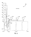
- FIGS. 3A-E show different embodiments of a memory array 300 that implements a scrubber.
- Memory array 300 -A ( FIG. 3A ) illustrates one scrubbing region that occupies an entire programmable logic IC.
- the scrubbing region includes an array of memory cells for configuration data 302 and check bits 304 and a data register with error correcting circuitry 308 .
- the scrubbing region includes multiple ECC blocks 306 that are each one column wide and span the entire height of the programmable logic IC.
- Memory array 300 -B ( FIG. 3B ) illustrates two scrubbing regions 310 .
- Each scrubbing region 310 spans the entire width and half the height of the programmable logic IC.
- Each scrubbing region 310 has a separate data register with error correcting circuitry 314 .
- Each scrubbing region 310 includes multiple ECC blocks 312 that are each one column wide and span half the height of the programmable logic IC.
- Memory array 300 -C ( FIG. 3C ) also illustrates two scrubbing regions 320 .
- Each scrubbing region 320 includes multiple ECC blocks 322 that are each two columns wide and span half the height of the programmable logic IC.
- Memory array 300 -D ( FIG. 3D ) illustrates four scrubbing regions 330 .
- Each scrubbing region 330 spans half the width and half the height of the programmable logic IC.
- Each scrubbing region 330 has a separate data register with error correcting circuitry 334 .
- Each scrubbing region 330 includes multiple ECC blocks 332 that are each one column wide and span half the height of the programmable logic IC.
- Memory array 300 -E ( FIG. 3E ) illustrates four scrubbing regions 340 (e.g., 340 - 1 , 340 - 2 , 340 - 3 , 340 - 4 ).
- Two scrubbing regions (e.g., 340 - 1 and 340 - 2 ; and 340 - 3 and 340 - 4 ) are interleaved in each half of the programmable logic IC such that the memory cells are physically non-contiguous (e.g., every other row of memory cells are part of the same scrubbing region).
- Each scrubbing region 340 spans the entire width and one-quarter the height of the programmable logic IC.
- Each scrubbing region 340 has a separate data register with error correcting circuitry 344 .
- Each scrubbing region 340 includes multiple ECC blocks 342 that are each two columns wide and span one-quarter the height of the programmable logic IC.
- Memory arrays 300 A-E are merely illustrative and described herein for clarity. However, the invention may be implemented using other numbers and arrangements of scrubbing regions and ECC blocks.
- the time in which an error is detected and corrected can be reduced by providing error correcting circuitry for some or all of the memory cells in a programmable logic IC.
- the error correcting circuitry can be continuously operative so that errors are corrected substantially as soon as they occur.
- memory cells in the programmable logic IC are divided into one or more ECC regions.
- Each ECC region includes a set of memory cells and dedicated error correcting circuitry that corrects errors that may occur in one or more memory cells.
- the memory cells of each ECC region are directly connected to the inputs of error correcting circuitry with the outputs directly driving the control point of the programmable logic IC (i.e., the outputs of the error correcting circuitry are driven onto corresponding data lines).
- the dedicated error correcting circuitry generates the correct value for a given memory cell. Since the error correcting circuitry does not physically change the contents of a given memory cell, other circuitry, such as a scrubber described above, can be used in conjunction with the dedicated error correcting circuitry to write the correct value into the given memory cell.
- the ECC regions may be the same as the scrubbing regions, in which case these regions may share the same error check bits. Alternatively, the ECC regions may be different from the scrubbing regions, in which case each region may require different error check bits.
- Each memory cell can be designed to have a small amount of associated logic that determines whether an error has occurred and generates the correct output if an error is detected.
- the associated logic forms an error correcting cell that can be replicated across the programmable logic IC to be associated with each memory cell.
- An extra column and row of memory cells e.g., parity cells
- the binary digit stored in the extra memory cell is the binary digit that makes the exclusive OR (XOR) of all the memory cells in that column or row a binary “0.”
- the binary digit stored in the extra memory cell is the binary digit that makes the XOR of all the memory cells in that column or row a binary “1.”
- a horizontal parity generator and a vertical parity generator can be used to detect errors that occur in a memory cell.
- Each error correcting cell XORs the data from a memory cell with the incoming horizontal and vertical parity lines and sends the result onto outgoing horizontal and vertical parity lines.
- a resulting horizontal parity for a row of memory cells and a resulting vertical parity for a column of memory cells are used to determine whether an error has occurred in the memory cell in the row and column. If an error has occurred (e.g., if the horizontal parity and the vertical parity are both binary “1”), the error correcting cell complements the data from the memory cell to generate the correct value at the output.
- a reasonable number of error correcting cells may be cascaded to form an array of a suitable size.
- a first input to the parity generator may be tied to ground (e.g., binary “0”) and the last output may be the resulting parity that is used to detect the occurrence of an error. If the ECC regions are small, it may be desirable to customize the error correcting cell at the ends of the array to eliminate unused logic (e.g., the XOR gate in the first cell that has an input tied to ground can therefore be replaced with a wire).
- error correcting circuitry 400 An illustration of error correcting circuitry 400 is shown in FIG. 4 .
- circuitry 400 is described in the context of a 2 ⁇ 2 array of memory cells 402 with an extra row and column of parity cells 404 .
- the invention can be implemented using other array sizes of memory cells 402 .
- Each memory cell 402 and parity cell 404 has an associated error correcting cell 410 that detects and corrects a data error.
- Each cell 410 also has two incoming horizontal parity lines 414 and 418 , one outgoing horizontal parity line 416 , two incoming vertical parity lines 420 and 424 , one outgoing vertical parity line 422 , and an output 434 that generates the correct value for the associated memory cell 402 or parity cell 404 .
- incoming horizontal parity line 414 is tied to ground (i.e., set to binary “0”).
- outgoing horizontal parity line 416 serves as incoming horizontal parity line 414 for adjacent cell 410 .
- outgoing horizontal parity line 416 which contains the computed parity of the row, serves as incoming horizontal parity line 418 for each cell 410 in the given row that is used to determine whether an error has occurred in that row.
- incoming vertical parity line 420 is tied to ground (i.e., set to binary “0”).
- outgoing vertical parity line 422 serves as incoming vertical parity line 420 for adjacent cell 410 .
- the outgoing vertical parity line which contains the computed parity of the column, serves as incoming vertical parity line 424 for each cell 410 in the given column that is used to determine whether an error has occurred in that column.
- Each cell 410 includes three XOR gates 426 , 428 , and 432 , and an AND gate 430 .
- XOR gate 426 has as inputs data 412 (e.g., from memory cell 402 or parity cell 404 ) and incoming horizontal parity line 414 , and outputs data on outgoing horizontal parity line 416 .
- XOR gate 428 has as inputs data 412 and incoming vertical parity line 420 , and outputs data on outgoing vertical parity line 422 .
- the computed horizontal parity, which is sent on incoming horizontal parity line 418 , and the computed vertical parity, which is sent on incoming vertical parity line 424 are input to AND gate 430 .
- Data 412 and the output of AND gate 430 are input to XOR gate 432 which sends as output 434 the correct output bit.
- Output 434 may be coupled to data lines (e.g., lines 250 ) so that the data can be sent to the data register.
- Static hazards may occur during the operation of the programmable logic IC.
- a static hazard is a property of a circuit in which a change in logic value of one input causes a momentarily incorrect value (e.g., a glitch) on one of its outputs. This can be attributed to the difference in propagation time for the inputs to XOR gate 432 .
- One input, data 412 comes directly from memory cell 402 or 404 .
- the other input requires the horizontal parity and vertical parity to be generated and propagated to AND gate 430 . If data from one memory cell changes, the change will be rapidly propagated to XOR gate 432 , causing a transition to an incorrect value at output 434 . Some time later, once the horizontal parity and vertical parity are generated, a second transition back to the correct value will occur at output 434 .
- error correcting circuitry can further be designed to reduce static hazards while limiting the amount of logic required to implement such error correcting circuitry.
- error correcting circuitry can be designed to avoid these reconvergent paths and thus reduce such hazards.
- a separate horizontal parity generator and vertical parity generator can be designed that compute the parity for all the memory cells in that row and column except for the particular memory cell being corrected. The correct value is then computed based on the horizontal parity, vertical parity, and the data from the particular memory cell.
- each memory cell requires additional logic for generating the parity of all the memory cells in a row or column except for the particular memory cell. For example, if there are N memory cells in a row or column, the parity for all the memory cells can be generated using (N ⁇ 1) XOR gates. It is possible to generate the parity of each one of a possible set of N memory cells by using a total of (3*N ⁇ 6) XOR gates. A first set of logic levels can generate the parity of each possible set of 2 K inputs for a subset of values of 2 K that are aligned with that particular power of 2 up to N/2.
- Subsequent logic stages can generate the parity of each possible set of (N—1) of the inputs.
- a 10-transistor complex gate e.g., OR-AND-OR gate or OR-AND-OR-INVERT gate
- OR-AND-OR gate OR-AND-OR-INVERT gate
- circuitry 500 is described in the context of a 3 ⁇ 3 array of memory cells 502 with an extra row and column of parity cells 504 , although the invention can be implemented using other array sizes of memory cells 502 .
- Each memory cell 502 and parity cell 504 has an associated error correcting cell 510 that detects and corrects a bit error.
- the contents of a particular memory cell 502 or parity cell 504 are sent as input 512 to an associated error correcting cell 510 .
- Each cell 510 also receives as input data 514 from the contents of the other cells 502 and/or 504 in the same column and data 516 from the contents of the other cells 502 and/or 504 in the same row.
- Data 514 is sent as input to circuitry 518 that generates the vertical parity (Vi) for the other cells 502 and/or 504 in that column.
- Data 516 is sent as input to circuitry 520 that generates the horizontal parity (Hi) for the other cells 502 and/or 504 in that row.
- each cell 510 is shown as having separate circuitry 518 and 520
- the memory cells 502 and parity cell(s) 504 in each column and row can share circuitry to compute the vertical and horizontal parity.
- the outputs of circuitry 518 and 520 are sent as input to a complex logic gate 522 .
- Complex logic gate 522 can be an OR-AND-OR gate.
- complex logic gate 522 can be an OR-AND-OR-INVERT gate in which the complement of the data is stored in cells 502 and 504 .
- Complex logic gate 522 generates a correct value for the particular memory cell 502 or parity cell 504 at output 530 .
- Circuitry 518 and 520 can be implemented using XOR gates.
- FIG. 6 shows an embodiment of circuitry 520 that computes the horizontal parity bit H 0 , H 1 , H 2 , and H 3 for all the cells 502 and/or 504 in the row except for the particular cell 502 or 504 being corrected.
- XOR gates 604 are used to generate the parity for two pairs of cells 502 and/or 504 (e.g., cell pairs 0 and 1 and cell pairs 2 and 3 ).
- XOR gates 606 are used to generate the parity for one of the pairs of cells and another cell that is not the particular cell being corrected.
- output H 0 is the parity of memory cells 1 , 2 , and 3 ;
- output H 1 is the parity of memory cells 0 , 2 , and 3 ;
- output H 2 is the parity of memory cells 0 , 1 , and 2 ;
- output H 3 is the parity of memory cells 0 , 1 , and 2 .
- a total of 6 i.e., 3*N ⁇ 6, where N is 4) XOR gates are used.
- a vertical parity bit can also be generated using similar logic levels.
- Hazard-free error correcting circuitry can also be implemented using the triple redundancy method which may require less logic gates and is thus less expensive to implement than the approach described in connection with FIGS. 5 and 6 .
- each configuration bit is programmed into three memory cells, which can be physically contiguous or physically non-contiguous.
- a hazard-free voting circuit includes a complex logic gate that compares the data stored in the three memory cells. The output of the circuitry is the same bit value stored in at least two of the memory cells. This circuitry produces a correct output when only one memory cell has an error. If more than one memory cell in the group of three memory cells has an error, an incorrect output will be generated.
- FIG. 7 An illustration of hazard-free error correcting circuitry 700 using the triple redundancy method is shown in FIG. 7 .
- a configuration data bit is stored in three memory cells 702 , 704 , and 706 .
- Data from memory cells 702 , 704 , and 706 are sent as input to a complex logic gate 710 .
- Complex logic gate 710 can be an OR-AND-OR gate.
- complex logic gate 710 can be an OR-AND-OR-INVERT gate in which the complement of the data is stored in cells 702 , 704 , and 706 .
- Complex logic gate 710 generates a correct value for the memory cells 702 , 704 , and 706 at output 720 .
- output 720 will still be a binary “1.”
- output 720 will be a binary “0.”
- the output of the gate would be the same value as the three memory cells 702 , 704 , and 706 , not the complement as described above.
- a further approach to reduce costs in implementing error correcting circuitry is to make a logic stage of the error correcting circuitry so slow that any potential glitch is absorbed by the logic.
- a logic gate with a weak drive, together with a large capacitive load can be added to the output of the error correcting circuitry.
- the logic gate may be weakened by using narrow and long transistors or by adding a resistive element at the output.
- the resistive element may be polysilicon wire, another high resistivity circuit structure, a current starved pass gate with both gates turned on at slightly above the threshold voltage, or a current starved inverter.
- FIGS. 8A-C An illustration of such circuitry 800 is shown in FIGS. 8A-C .
- Data from a memory cell or parity cell 802 is sent to a cell 810 containing error correcting circuitry (e.g., cell 410 or 510 ).
- the output of cell 810 can be sent to a resistive element such as a resistor 812 ( FIG. 8A ), a current starved pass gate 820 ( FIG. 8B ), a current starved inverter 830 ( FIG. 8C ), or other resistive element, together with a capacitive load 814 , increases the delay time.
- the output of the resistive element has the correct value for output onto a data line.
- FIG. 9A is a diagram of a 12:1 multiplexer 900 commonly used in programmable logic IC routing architectures.
- Multiplexer 900 can be constructed as a two-stage random access memory (RAM) sharing multiplexer.
- the first stage includes three 4:1 multiplexers 902 .
- the second stage includes one 3:1 multiplexer 904 .
- Seven memory cells 906 are needed to configure multiplexer 900 .
- FIG. 9B is a diagram of a 12:1 multiplexer 910 with error correcting circuitry 912 . Additional memory cells 914 are needed to store error check bits for performing error correction.
- FIG. 9C is a diagram of a fully encoded 12:1 multiplexer 920 .
- Multiplexer 920 requires two 2:4 decoders 922 and 924 : one for interfacing the three 4:1 multiplexers 902 with error correcting circuitry 926 , and one for interfacing the 3:1 multiplexer 904 with error correcting circuitry 926 . Because of the use of decoders 922 and 924 , fewer memory cells 928 are needed to control the operation of multiplexer 920 . A fully encoded multiplexer 920 is more efficient when error correcting circuitry 926 is included.
- error correcting circuitry can also be provided to correct errors occurring in embedded memory blocks (EMBs) in a programmable logic IC.
- EMBs embedded memory blocks
- error correcting circuitry can be included in the input and output interface circuitry.
- FIG. 10 illustrates one embodiment of an EMB 1000 with error correcting circuitry implemented in hardware.
- Input data 1002 is sent to an interface 1004 in EMB 1000 .
- Data from interface 1004 is sent to a memory array, read and write circuitry 1008 and an ECC generator 1006 .
- ECC generator 1006 on the input (i.e., write) circuitry of the EMB computes error check bits for the input data. For example, for N data bits, M error check bits may be required (e.g., with M ⁇ log(N+M+1)).
- the error check bits are sent as input to memory array, read and write circuitry 1008 where the error check bits are stored.
- Data from memory array, read and write circuitry 1008 is sent as input to a multiplexer 1012 and an ECC corrector 1010 .
- ECC corrector on the output (i.e., read) circuitry of EMB 1000 determines whether an error has occurred in the data based on the error check bits and corrects any errors before sending the data to multiplexer 1012 .
- ECC corrector 1010 can include any suitable error correcting code including, for example, a Hamming Code, Reed-Solomon Code, and Product Code.
- Multiplexer 1012 selects one of the inputs for output to interface 1014 .
- Data 1016 is then output from EMB 1000 .
- ECC hardware e.g., ECC generator 1006 and ECC corrector 1010
- ECC generator 1006 and ECC corrector 1010 ECC generator 1006 and ECC corrector 1010
- FIG. 11 illustrates another embodiment of an EMB 1100 with error correcting circuitry implemented in soft logic.
- An ECC generator 1102 and ECC corrector 1104 can be implemented outside of EMB 1100 by a computer aided design (CAD) system in the soft logic (e.g., using logic elements) of the programmable logic IC.
- CAD computer aided design
- an EMB 1100 that provides read/write access to 8-bit wide words should also be able to provide access to 12-bit wide words to support the storage of error-corrected 8-bit wide words (e.g., 8 data bits and 4 error check bits per word).
- Implementing error correcting circuitry in soft logic ( FIG. 11 ) rather than in hard logic ( FIG. 10 ) advantageously reduces the required size of the programmable logic IC. However, using soft logic results in slower logic that consumes soft logic resources.
- FIG. 12 illustrates a programmable logic IC 1202 , multi-chip module 1204 , or other device (e.g., ASSP, ASIC, full-custom chip, dedicated chip). which includes embodiments of this invention in a data processing system 1200 .
- Data processing system 1200 can include one or more of the following components: a processor 1206 , memory 1208 , I/O circuitry 1210 , and peripheral devices 1212 . These components are coupled together by a system bus or other interconnections 1220 and are populated on a circuit board 1230 which is contained in an end-user system 1240 .
- System 1200 can be used in a wide variety of applications, such as computer networking, data networking, instrumentation, video processing, digital signal processing, or any other application where the advantage of using programmable or reprogrammable logic is desirable.
- Programmable logic IC/module 1202 / 1204 can be used to perform a variety of different logic functions.
- programmable logic IC/module 1202 / 1204 can be configured as a processor or controller that works in cooperation with processor 1206 .
- Programmable logic IC/module 1202 / 1204 may also be used as an arbiter for arbitrating access to a shared IC in system 1200 .
- programmable logic IC/module 1202 / 1204 can be configured as an interface between processor 1206 and one of the other components in system 1200 . It should be noted that system 1200 is only exemplary, and that the true scope and spirit of the invention should be indicated by the following claims.
- circuitry that detects and corrects errors in programmable logic ICs.
Abstract
Description
Z=NOT((Hi AND Vi)OR(C AND(Hi OR Vi))) (1)
-
- C=
Data 512 - Hi=Horizontal parity from 520
- Vi=Vertical parity from 518.
- C=
Claims (23)
Priority Applications (1)
| Application Number | Priority Date | Filing Date | Title |
|---|---|---|---|
| US11/955,910 US8112678B1 (en) | 2004-01-27 | 2007-12-13 | Error correction for programmable logic integrated circuits |
Applications Claiming Priority (2)
| Application Number | Priority Date | Filing Date | Title |
|---|---|---|---|
| US10/766,464 US7328377B1 (en) | 2004-01-27 | 2004-01-27 | Error correction for programmable logic integrated circuits |
| US11/955,910 US8112678B1 (en) | 2004-01-27 | 2007-12-13 | Error correction for programmable logic integrated circuits |
Related Parent Applications (1)
| Application Number | Title | Priority Date | Filing Date |
|---|---|---|---|
| US10/766,464 Continuation US7328377B1 (en) | 2004-01-27 | 2004-01-27 | Error correction for programmable logic integrated circuits |
Publications (1)
| Publication Number | Publication Date |
|---|---|
| US8112678B1 true US8112678B1 (en) | 2012-02-07 |
Family
ID=38988924
Family Applications (2)
| Application Number | Title | Priority Date | Filing Date |
|---|---|---|---|
| US10/766,464 Expired - Fee Related US7328377B1 (en) | 2004-01-27 | 2004-01-27 | Error correction for programmable logic integrated circuits |
| US11/955,910 Expired - Fee Related US8112678B1 (en) | 2004-01-27 | 2007-12-13 | Error correction for programmable logic integrated circuits |
Family Applications Before (1)
| Application Number | Title | Priority Date | Filing Date |
|---|---|---|---|
| US10/766,464 Expired - Fee Related US7328377B1 (en) | 2004-01-27 | 2004-01-27 | Error correction for programmable logic integrated circuits |
Country Status (1)
| Country | Link |
|---|---|
| US (2) | US7328377B1 (en) |
Cited By (8)
| Publication number | Priority date | Publication date | Assignee | Title |
|---|---|---|---|---|
| US20100269022A1 (en) * | 2008-11-26 | 2010-10-21 | Arizona Board of Regents, for and behalf of Arizona State University | Circuits And Methods For Dual Redundant Register Files With Error Detection And Correction Mechanisms |
| US20110022930A1 (en) * | 2009-07-24 | 2011-01-27 | Shusaku Uchibori | Error correction circuit and error correction method |
| US20130145225A1 (en) * | 2011-12-01 | 2013-06-06 | Shenzhen China Star Optoelectronics Technology Co., Ltd. | Code checking method for a memory of a printed circuit board |
| US20150161323A1 (en) * | 2013-12-06 | 2015-06-11 | Robert Bosch Gmbh | Method for checking a hardware-configurable logic circuit for faults |
| US9450609B1 (en) | 2015-03-31 | 2016-09-20 | Altera Corporation | Methods and apparatus for embedding an error correction code in memory cells |
| US9703630B2 (en) | 2015-06-08 | 2017-07-11 | International Business Machines Corporation | Selective error coding |
| CN108090022A (en) * | 2016-11-22 | 2018-05-29 | 英特尔公司 | It is useful for the programmable integrated circuit of the stacked memory tube core of storage configuration data |
| US10564866B2 (en) | 2014-06-11 | 2020-02-18 | International Business Machines Corporation | Bank-level fault management in a memory system |
Families Citing this family (94)
| Publication number | Priority date | Publication date | Assignee | Title |
|---|---|---|---|---|
| DE60204539D1 (en) * | 2002-04-03 | 2005-07-14 | Sgs Thomson Microelectronics | Field programmable device |
| US7328377B1 (en) * | 2004-01-27 | 2008-02-05 | Altera Corporation | Error correction for programmable logic integrated circuits |
| US7426678B1 (en) * | 2004-07-20 | 2008-09-16 | Xilinx, Inc. | Error checking parity and syndrome of a block of data with relocated parity bits |
| JP4643977B2 (en) * | 2004-11-30 | 2011-03-02 | 富士通株式会社 | Programmable logic device, information processing apparatus, and control method for programmable logic device |
| US20060133607A1 (en) * | 2004-12-22 | 2006-06-22 | Seagate Technology Llc | Apparatus and method for generating a secret key |
| FR2883998A1 (en) * | 2005-04-05 | 2006-10-06 | St Microelectronics Sa | Coprocessor`s control execution securing method for e.g. microcontroller, involves placing coprocessor in default error mode from commencement of execution of control accomplished by coprocessor |
| US7430703B1 (en) * | 2005-05-24 | 2008-09-30 | Xilinx, Inc. | Error correction for multiple word read |
| US7581154B2 (en) * | 2005-06-30 | 2009-08-25 | Intel Corporation | Method and apparatus to lower operating voltages for memory arrays using error correcting codes |
| US7550858B1 (en) * | 2005-07-19 | 2009-06-23 | Xilinx, Inc. | Random sequence generation using alpha particle emission |
| US7702978B2 (en) * | 2006-04-21 | 2010-04-20 | Altera Corporation | Soft error location and sensitivity detection for programmable devices |
| US7917828B2 (en) * | 2006-12-28 | 2011-03-29 | Intel Corporation | Providing error correction coding for probed data |
| US8775717B2 (en) | 2007-12-27 | 2014-07-08 | Sandisk Enterprise Ip Llc | Storage controller for flash memory including a crossbar switch connecting a plurality of processors with a plurality of internal memories |
| KR20090096026A (en) * | 2008-03-07 | 2009-09-10 | 삼성전자주식회사 | Apparatus and method for communicating multicast and broadcast service map message in a broadband wireless communication system |
| US8739010B2 (en) * | 2010-11-19 | 2014-05-27 | Altera Corporation | Memory array with redundant bits and memory element voting circuits |
| US8522126B1 (en) | 2010-12-22 | 2013-08-27 | Lattice Semiconductor Corporation | Blocking memory readback in a programmable logic device |
| US8984367B2 (en) | 2011-02-25 | 2015-03-17 | Altera Corporation | Error detection and correction circuitry |
| US8909982B2 (en) | 2011-06-19 | 2014-12-09 | Sandisk Enterprise Ip Llc | System and method for detecting copyback programming problems |
| US8910020B2 (en) | 2011-06-19 | 2014-12-09 | Sandisk Enterprise Ip Llc | Intelligent bit recovery for flash memory |
| US8938658B2 (en) * | 2011-11-07 | 2015-01-20 | Sandisk Enterprise Ip Llc | Statistical read comparison signal generation for memory systems |
| US8954822B2 (en) | 2011-11-18 | 2015-02-10 | Sandisk Enterprise Ip Llc | Data encoder and decoder using memory-specific parity-check matrix |
| US8924815B2 (en) | 2011-11-18 | 2014-12-30 | Sandisk Enterprise Ip Llc | Systems, methods and devices for decoding codewords having multiple parity segments |
| US9048876B2 (en) | 2011-11-18 | 2015-06-02 | Sandisk Enterprise Ip Llc | Systems, methods and devices for multi-tiered error correction |
| US9699263B1 (en) | 2012-08-17 | 2017-07-04 | Sandisk Technologies Llc. | Automatic read and write acceleration of data accessed by virtual machines |
| US9501398B2 (en) | 2012-12-26 | 2016-11-22 | Sandisk Technologies Llc | Persistent storage device with NVRAM for staging writes |
| US9612948B2 (en) | 2012-12-27 | 2017-04-04 | Sandisk Technologies Llc | Reads and writes between a contiguous data block and noncontiguous sets of logical address blocks in a persistent storage device |
| US9239751B1 (en) | 2012-12-27 | 2016-01-19 | Sandisk Enterprise Ip Llc | Compressing data from multiple reads for error control management in memory systems |
| US9454420B1 (en) | 2012-12-31 | 2016-09-27 | Sandisk Technologies Llc | Method and system of reading threshold voltage equalization |
| US9003264B1 (en) | 2012-12-31 | 2015-04-07 | Sandisk Enterprise Ip Llc | Systems, methods, and devices for multi-dimensional flash RAID data protection |
| US9329928B2 (en) | 2013-02-20 | 2016-05-03 | Sandisk Enterprise IP LLC. | Bandwidth optimization in a non-volatile memory system |
| US9214965B2 (en) | 2013-02-20 | 2015-12-15 | Sandisk Enterprise Ip Llc | Method and system for improving data integrity in non-volatile storage |
| US9870830B1 (en) | 2013-03-14 | 2018-01-16 | Sandisk Technologies Llc | Optimal multilevel sensing for reading data from a storage medium |
| US9136877B1 (en) | 2013-03-15 | 2015-09-15 | Sandisk Enterprise Ip Llc | Syndrome layered decoding for LDPC codes |
| US9244763B1 (en) | 2013-03-15 | 2016-01-26 | Sandisk Enterprise Ip Llc | System and method for updating a reading threshold voltage based on symbol transition information |
| US9009576B1 (en) | 2013-03-15 | 2015-04-14 | Sandisk Enterprise Ip Llc | Adaptive LLR based on syndrome weight |
| US9236886B1 (en) | 2013-03-15 | 2016-01-12 | Sandisk Enterprise Ip Llc | Universal and reconfigurable QC-LDPC encoder |
| US9092350B1 (en) | 2013-03-15 | 2015-07-28 | Sandisk Enterprise Ip Llc | Detection and handling of unbalanced errors in interleaved codewords |
| US9367246B2 (en) | 2013-03-15 | 2016-06-14 | Sandisk Technologies Inc. | Performance optimization of data transfer for soft information generation |
| US10049037B2 (en) | 2013-04-05 | 2018-08-14 | Sandisk Enterprise Ip Llc | Data management in a storage system |
| US9170941B2 (en) | 2013-04-05 | 2015-10-27 | Sandisk Enterprises IP LLC | Data hardening in a storage system |
| US9159437B2 (en) | 2013-06-11 | 2015-10-13 | Sandisk Enterprise IP LLC. | Device and method for resolving an LM flag issue |
| US9384126B1 (en) | 2013-07-25 | 2016-07-05 | Sandisk Technologies Inc. | Methods and systems to avoid false negative results in bloom filters implemented in non-volatile data storage systems |
| US9524235B1 (en) | 2013-07-25 | 2016-12-20 | Sandisk Technologies Llc | Local hash value generation in non-volatile data storage systems |
| US9043517B1 (en) | 2013-07-25 | 2015-05-26 | Sandisk Enterprise Ip Llc | Multipass programming in buffers implemented in non-volatile data storage systems |
| US9361221B1 (en) | 2013-08-26 | 2016-06-07 | Sandisk Technologies Inc. | Write amplification reduction through reliable writes during garbage collection |
| US9639463B1 (en) | 2013-08-26 | 2017-05-02 | Sandisk Technologies Llc | Heuristic aware garbage collection scheme in storage systems |
| US9519577B2 (en) | 2013-09-03 | 2016-12-13 | Sandisk Technologies Llc | Method and system for migrating data between flash memory devices |
| US9442670B2 (en) | 2013-09-03 | 2016-09-13 | Sandisk Technologies Llc | Method and system for rebalancing data stored in flash memory devices |
| US9158349B2 (en) | 2013-10-04 | 2015-10-13 | Sandisk Enterprise Ip Llc | System and method for heat dissipation |
| US9298608B2 (en) | 2013-10-18 | 2016-03-29 | Sandisk Enterprise Ip Llc | Biasing for wear leveling in storage systems |
| US9442662B2 (en) | 2013-10-18 | 2016-09-13 | Sandisk Technologies Llc | Device and method for managing die groups |
| US9436831B2 (en) | 2013-10-30 | 2016-09-06 | Sandisk Technologies Llc | Secure erase in a memory device |
| US9263156B2 (en) | 2013-11-07 | 2016-02-16 | Sandisk Enterprise Ip Llc | System and method for adjusting trip points within a storage device |
| US9244785B2 (en) | 2013-11-13 | 2016-01-26 | Sandisk Enterprise Ip Llc | Simulated power failure and data hardening |
| US9152555B2 (en) | 2013-11-15 | 2015-10-06 | Sandisk Enterprise IP LLC. | Data management with modular erase in a data storage system |
| US9703816B2 (en) | 2013-11-19 | 2017-07-11 | Sandisk Technologies Llc | Method and system for forward reference logging in a persistent datastore |
| US9520197B2 (en) | 2013-11-22 | 2016-12-13 | Sandisk Technologies Llc | Adaptive erase of a storage device |
| US9520162B2 (en) | 2013-11-27 | 2016-12-13 | Sandisk Technologies Llc | DIMM device controller supervisor |
| US9582058B2 (en) | 2013-11-29 | 2017-02-28 | Sandisk Technologies Llc | Power inrush management of storage devices |
| US9235245B2 (en) | 2013-12-04 | 2016-01-12 | Sandisk Enterprise Ip Llc | Startup performance and power isolation |
| US9129665B2 (en) | 2013-12-17 | 2015-09-08 | Sandisk Enterprise Ip Llc | Dynamic brownout adjustment in a storage device |
| US9549457B2 (en) | 2014-02-12 | 2017-01-17 | Sandisk Technologies Llc | System and method for redirecting airflow across an electronic assembly |
| US9497889B2 (en) | 2014-02-27 | 2016-11-15 | Sandisk Technologies Llc | Heat dissipation for substrate assemblies |
| US9703636B2 (en) | 2014-03-01 | 2017-07-11 | Sandisk Technologies Llc | Firmware reversion trigger and control |
| US9348377B2 (en) | 2014-03-14 | 2016-05-24 | Sandisk Enterprise Ip Llc | Thermal isolation techniques |
| US9485851B2 (en) | 2014-03-14 | 2016-11-01 | Sandisk Technologies Llc | Thermal tube assembly structures |
| US9519319B2 (en) | 2014-03-14 | 2016-12-13 | Sandisk Technologies Llc | Self-supporting thermal tube structure for electronic assemblies |
| US9454448B2 (en) | 2014-03-19 | 2016-09-27 | Sandisk Technologies Llc | Fault testing in storage devices |
| US9390814B2 (en) | 2014-03-19 | 2016-07-12 | Sandisk Technologies Llc | Fault detection and prediction for data storage elements |
| US9448876B2 (en) | 2014-03-19 | 2016-09-20 | Sandisk Technologies Llc | Fault detection and prediction in storage devices |
| US9390021B2 (en) | 2014-03-31 | 2016-07-12 | Sandisk Technologies Llc | Efficient cache utilization in a tiered data structure |
| US9626400B2 (en) | 2014-03-31 | 2017-04-18 | Sandisk Technologies Llc | Compaction of information in tiered data structure |
| US9626399B2 (en) | 2014-03-31 | 2017-04-18 | Sandisk Technologies Llc | Conditional updates for reducing frequency of data modification operations |
| US9697267B2 (en) | 2014-04-03 | 2017-07-04 | Sandisk Technologies Llc | Methods and systems for performing efficient snapshots in tiered data structures |
| US10656842B2 (en) | 2014-05-30 | 2020-05-19 | Sandisk Technologies Llc | Using history of I/O sizes and I/O sequences to trigger coalesced writes in a non-volatile storage device |
| US8891303B1 (en) | 2014-05-30 | 2014-11-18 | Sandisk Technologies Inc. | Method and system for dynamic word line based configuration of a three-dimensional memory device |
| US10146448B2 (en) | 2014-05-30 | 2018-12-04 | Sandisk Technologies Llc | Using history of I/O sequences to trigger cached read ahead in a non-volatile storage device |
| US10162748B2 (en) | 2014-05-30 | 2018-12-25 | Sandisk Technologies Llc | Prioritizing garbage collection and block allocation based on I/O history for logical address regions |
| US10656840B2 (en) | 2014-05-30 | 2020-05-19 | Sandisk Technologies Llc | Real-time I/O pattern recognition to enhance performance and endurance of a storage device |
| US9093160B1 (en) | 2014-05-30 | 2015-07-28 | Sandisk Technologies Inc. | Methods and systems for staggered memory operations |
| US9070481B1 (en) | 2014-05-30 | 2015-06-30 | Sandisk Technologies Inc. | Internal current measurement for age measurements |
| US9703491B2 (en) | 2014-05-30 | 2017-07-11 | Sandisk Technologies Llc | Using history of unaligned writes to cache data and avoid read-modify-writes in a non-volatile storage device |
| US9645749B2 (en) | 2014-05-30 | 2017-05-09 | Sandisk Technologies Llc | Method and system for recharacterizing the storage density of a memory device or a portion thereof |
| US10372613B2 (en) | 2014-05-30 | 2019-08-06 | Sandisk Technologies Llc | Using sub-region I/O history to cache repeatedly accessed sub-regions in a non-volatile storage device |
| US10114557B2 (en) | 2014-05-30 | 2018-10-30 | Sandisk Technologies Llc | Identification of hot regions to enhance performance and endurance of a non-volatile storage device |
| US9652381B2 (en) | 2014-06-19 | 2017-05-16 | Sandisk Technologies Llc | Sub-block garbage collection |
| US9443601B2 (en) | 2014-09-08 | 2016-09-13 | Sandisk Technologies Llc | Holdup capacitor energy harvesting |
| US9638549B2 (en) * | 2014-10-31 | 2017-05-02 | Ememory Technology Inc. | Integrated capacitance sensing module and associated system |
| US20160179611A1 (en) * | 2014-12-23 | 2016-06-23 | Thuyen Le | Low overhead error checking and correction apparatus and method |
| KR102435181B1 (en) * | 2015-11-16 | 2022-08-23 | 삼성전자주식회사 | Semiconductor memory device, memory system including the same and method of operating memory system |
| KR20180009076A (en) * | 2016-07-18 | 2018-01-26 | 에스케이하이닉스 주식회사 | Semiconductor device and semiconductor system |
| US10446251B2 (en) | 2017-04-12 | 2019-10-15 | Intel Corporation | Methods and apparatus for detecting defects in memory circuitry |
| US11281195B2 (en) | 2017-09-29 | 2022-03-22 | Intel Corporation | Integrated circuits with in-field diagnostic and repair capabilities |
| US11182244B2 (en) * | 2018-10-16 | 2021-11-23 | Micron Technology, Inc. | Error correction management for a memory device |
| CN111259459A (en) * | 2020-02-20 | 2020-06-09 | 福建师范大学 | Deployment, storage, acquisition and arbitration method for important data in mobile terminal |
Citations (94)
| Publication number | Priority date | Publication date | Assignee | Title |
|---|---|---|---|---|
| US4005405A (en) | 1975-05-07 | 1977-01-25 | Data General Corporation | Error detection and correction in data processing systems |
| US4375664A (en) | 1980-06-03 | 1983-03-01 | Burroughs Corporation | Apparatus for detecting, correcting and logging single bit memory read errors using syndrome generating and decoding circuitry |
| US4866717A (en) | 1986-07-29 | 1989-09-12 | Matsushita Electric Industrial Co., Ltd. | Code error detecting and correcting apparatus |
| US4930098A (en) | 1988-12-30 | 1990-05-29 | Intel Corporation | Shift register programming for a programmable logic device |
| US4930107A (en) | 1988-08-08 | 1990-05-29 | Altera Corporation | Method and apparatus for programming and verifying programmable elements in programmable devices |
| US4940909A (en) | 1989-05-12 | 1990-07-10 | Plus Logic, Inc. | Configuration control circuit for programmable logic devices |
| US5111464A (en) | 1989-12-01 | 1992-05-05 | Mips Computer Systems, Inc. | Interrupt reporting for single-bit memory errors |
| US5200920A (en) | 1990-02-08 | 1993-04-06 | Altera Corporation | Method for programming programmable elements in programmable devices |
| US5237219A (en) | 1992-05-08 | 1993-08-17 | Altera Corporation | Methods and apparatus for programming cellular programmable logic integrated circuits |
| EP0291167B1 (en) | 1987-04-14 | 1994-01-19 | Matsushita Electric Industrial Co., Ltd. | A code error detecting method |
| US5291079A (en) | 1992-07-23 | 1994-03-01 | Xilinx, Inc. | Configuration control unit for programming a field programmable gate array and reading array status |
| US5305324A (en) | 1990-09-26 | 1994-04-19 | Demografx | Data scrambling interface for correcting large burst errors in high speed, high capacity tape drives |
| US5321704A (en) | 1991-01-16 | 1994-06-14 | Xilinx, Inc. | Error detection structure and method using partial polynomial check |
| US5349691A (en) | 1990-07-03 | 1994-09-20 | Xilinx, Inc. | Programming process for 3-level programming logic devices |
| US5426379A (en) | 1994-07-29 | 1995-06-20 | Xilinx, Inc. | Field programmable gate array with built-in bitstream data expansion |
| US5430687A (en) | 1994-04-01 | 1995-07-04 | Xilinx, Inc. | Programmable logic device including a parallel input device for loading memory cells |
| US5466117A (en) | 1993-06-10 | 1995-11-14 | Xilinx, Inc. | Device and method for programming multiple arrays of semiconductor devices |
| US5495491A (en) | 1993-03-05 | 1996-02-27 | Motorola, Inc. | System using a memory controller controlling an error correction means to detect and correct memory errors when and over a time interval indicated by registers in the memory controller |
| US5511211A (en) | 1988-08-31 | 1996-04-23 | Hitachi, Ltd. | Method for flexibly developing a data processing system comprising rewriting instructions in non-volatile memory elements after function check indicates failure of required functions |
| US5528176A (en) | 1992-11-05 | 1996-06-18 | Xilinx, Inc. | Register with duplicate decoders for configurable cellular array |
| US5543730A (en) | 1995-05-17 | 1996-08-06 | Altera Corporation | Techniques for programming programmable logic array devices |
| US5581198A (en) | 1995-02-24 | 1996-12-03 | Xilinx, Inc. | Shadow DRAM for programmable logic devices |
| US5588112A (en) | 1992-12-30 | 1996-12-24 | Digital Equipment Corporation | DMA controller for memory scrubbing |
| US5590305A (en) | 1994-03-28 | 1996-12-31 | Altera Corporation | Programming circuits and techniques for programming logic |
| US5598530A (en) | 1993-02-16 | 1997-01-28 | Fujitsu Limited | Method and apparatus for controlling using checksums execution of object programs |
| US5606276A (en) | 1994-10-05 | 1997-02-25 | Altera Corporation | Method and apparatus for creating a large delay in a pulse in a layout efficient manner |
| US5608342A (en) | 1995-10-23 | 1997-03-04 | Xilinx, Inc. | Hierarchical programming of electrically configurable integrated circuits |
| US5629949A (en) | 1993-09-21 | 1997-05-13 | Cirrus Logic, Inc. | Error correction verification method and apparatus using CRC check remainders |
| US5640106A (en) | 1995-05-26 | 1997-06-17 | Xilinx, Inc. | Method and structure for loading data into several IC devices |
| US5650734A (en) | 1995-12-11 | 1997-07-22 | Altera Corporation | Programming programmable transistor devices using state machines |
| US5694399A (en) | 1996-04-10 | 1997-12-02 | Xilinix, Inc. | Processing unit for generating signals for communication with a test access port |
| US5694056A (en) | 1996-04-01 | 1997-12-02 | Xilinx, Inc. | Fast pipeline frame full detector |
| US5742531A (en) | 1996-05-03 | 1998-04-21 | Xilinx Inc | Configurable parallel and bit serial load apparatus |
| EP0838969A2 (en) | 1996-10-24 | 1998-04-29 | AT&T Corp. | Fast framing of the ATM protocol used alone by header error check |
| US5754566A (en) | 1996-09-06 | 1998-05-19 | Intel Corporation | Method and apparatus for correcting a multilevel cell memory by using interleaving |
| US5767734A (en) | 1995-12-21 | 1998-06-16 | Altera Corporation | High-voltage pump with initiation scheme |
| US5773993A (en) | 1996-09-26 | 1998-06-30 | Xilinx, Inc. | Configurable electronic device which is compatible with a configuration bitstream of a prior generation configurable electronic device |
| US5821772A (en) | 1996-08-07 | 1998-10-13 | Xilinx, Inc. | Programmable address decoder for programmable logic device |
| US5844854A (en) | 1996-09-18 | 1998-12-01 | Altera Corporation | Programmable logic device with two dimensional memory addressing |
| US5873113A (en) | 1996-09-24 | 1999-02-16 | Altera Corporation | System and method for programming eprom cells using shorter duration pulse(s) in repeating the programming process of a particular cell |
| US5949987A (en) | 1995-08-09 | 1999-09-07 | Xilinx, Inc. | Efficient in-system programming structure and method for non-volatile programmable logic devices |
| US5961576A (en) | 1996-05-03 | 1999-10-05 | Xilinx, Inc. | Configurable parallel and bit serial load apparatus |
| US5978952A (en) | 1996-12-31 | 1999-11-02 | Intel Corporation | Time-distributed ECC scrubbing to correct memory errors |
| US5995744A (en) | 1997-11-24 | 1999-11-30 | Xilinx, Inc. | Network configuration of programmable circuits |
| US5995988A (en) | 1997-12-04 | 1999-11-30 | Xilinx, Inc. | Configurable parallel and bit serial load apparatus |
| US5999014A (en) | 1997-09-17 | 1999-12-07 | Xilinx, Inc. | Method for concurrently programming or accessing a plurality of in-system-programmable logic devices |
| US6011406A (en) | 1997-10-28 | 2000-01-04 | Altera Corporation | Ultra-fast configuration mode for a programmable logic device |
| US6018250A (en) | 1997-06-26 | 2000-01-25 | Xilinx, Inc. | Programming method to enable system recovery after power failure |
| US6023565A (en) | 1996-03-29 | 2000-02-08 | Xilinx, Inc. | Method for configuring circuits over a data communications link |
| US6024486A (en) | 1996-06-05 | 2000-02-15 | Compaq Computer Corporation | Data error detection and correction |
| US6028445A (en) | 1997-12-30 | 2000-02-22 | Xilinx, Inc. | Decoder structure and method for FPGA configuration |
| US6044025A (en) | 1999-02-04 | 2000-03-28 | Xilinx, Inc. | PROM with built-in JTAG capability for configuring FPGAs |
| US6049222A (en) | 1997-12-30 | 2000-04-11 | Xilinx, Inc | Configuring an FPGA using embedded memory |
| US6057704A (en) | 1997-12-12 | 2000-05-02 | Xilinx, Inc. | Partially reconfigurable FPGA and method of operating same |
| US6065146A (en) | 1996-10-21 | 2000-05-16 | Texas Instruments Incorporated | Error correcting memory |
| US6069489A (en) | 1998-08-04 | 2000-05-30 | Xilinx, Inc. | FPGA having fast configuration memory data readback |
| US6097210A (en) | 1998-08-04 | 2000-08-01 | Xilinx, Inc. | Multiplexer array with shifted input traces |
| US6101614A (en) | 1994-05-24 | 2000-08-08 | Intel Corporation | Method and apparatus for automatically scrubbing ECC errors in memory via hardware |
| US6105105A (en) | 1996-07-19 | 2000-08-15 | Xilinx, Inc. | Data processing system using configuration select logic, an instruction store, and sequencing logic during instruction execution |
| US6128215A (en) | 1997-08-19 | 2000-10-03 | Altera Corporation | Static random access memory circuits |
| US6137307A (en) | 1998-08-04 | 2000-10-24 | Xilinx, Inc. | Structure and method for loading wide frames of data from a narrow input bus |
| US6191614B1 (en) | 1999-04-05 | 2001-02-20 | Xilinx, Inc. | FPGA configuration circuit including bus-based CRC register |
| US6204687B1 (en) | 1999-08-13 | 2001-03-20 | Xilinx, Inc. | Method and structure for configuring FPGAS |
| US6216259B1 (en) | 1997-08-28 | 2001-04-10 | Xilinx, Inc. | Configuration of programmable logic devices with routing core generators |
| US6223309B1 (en) | 1998-10-02 | 2001-04-24 | International Business Machines Corporation | Method and apparatus for ECC logic test |
| EP1100020A1 (en) | 1999-04-22 | 2001-05-16 | Matsushita Electric Industrial Co., Ltd. | Processor |
| US6237124B1 (en) | 1998-03-16 | 2001-05-22 | Actel Corporation | Methods for errors checking the configuration SRAM and user assignable SRAM data in a field programmable gate array |
| US6242941B1 (en) | 1998-05-29 | 2001-06-05 | Altera Corporation | Reducing I/O noise when leaving programming mode |
| US6279128B1 (en) | 1994-12-29 | 2001-08-21 | International Business Machines Corporation | Autonomous system for recognition of patterns formed by stored data during computer memory scrubbing |
| US6314550B1 (en) | 1997-06-10 | 2001-11-06 | Altera Corporation | Cascaded programming with multiple-purpose pins |
| US6349390B1 (en) | 1999-01-04 | 2002-02-19 | International Business Machines Corporation | On-board scrubbing of soft errors memory module |
| US6429682B1 (en) | 1999-04-05 | 2002-08-06 | Xilinx, Inc. | Configuration bus interface circuit for FPGAs |
| US20030097628A1 (en) | 2001-10-11 | 2003-05-22 | Ngo Ninh D. | Error detection on programmable logic resources |
| US6701480B1 (en) | 2000-03-08 | 2004-03-02 | Rockwell Automation Technologies, Inc. | System and method for providing error check and correction in memory systems |
| US20040230767A1 (en) | 2000-08-31 | 2004-11-18 | International Business Machines Corporation | Low cost and high ras mirrored memory |
| US6832340B2 (en) | 2000-01-26 | 2004-12-14 | Hewlett-Packard Development Company, L.P. | Real-time hardware memory scrubbing |
| US6838899B2 (en) | 2002-12-30 | 2005-01-04 | Actel Corporation | Apparatus and method of error detection and correction in a radiation-hardened static random access memory field-programmable gate array |
| US6839868B1 (en) | 1998-10-12 | 2005-01-04 | Centre National D'etudes Spatiales | Method for processing an electronic system subjected to transient error constraints and memory access monitoring device |
| US6845472B2 (en) * | 2000-01-25 | 2005-01-18 | Hewlett-Packard Development Company, L.P. | Memory sub-system error cleansing |
| US6848063B2 (en) | 2001-11-20 | 2005-01-25 | Hewlett-Packard Development Company, L.P. | System and method for scrubbing errors in very large memories |
| US6847554B2 (en) | 2002-08-02 | 2005-01-25 | Sony Corporation | Nonvolatile semiconductor memory device with error detection and correction circuit |
| US6859904B2 (en) | 2001-05-11 | 2005-02-22 | Sun Microsystems, Inc. | Apparatus and method to facilitate self-correcting memory |
| US20050044467A1 (en) | 2001-11-14 | 2005-02-24 | Wingyu Leung | Transparent error correcting memory |
| US20050073884A1 (en) | 2003-10-03 | 2005-04-07 | Gonzalez Carlos J. | Flash memory data correction and scrub techniques |
| US20050144551A1 (en) | 2003-12-16 | 2005-06-30 | Nahas Joseph J. | MRAM having error correction code circuitry and method therefor |
| US20050154943A1 (en) | 2003-12-29 | 2005-07-14 | Alexander James W. | Mechanism for adjacent-symbol error correction and detection |
| US7007203B2 (en) | 2002-08-02 | 2006-02-28 | Motorola, Inc. | Error checking in a reconfigurable logic signal processor (RLSP) |
| US7030647B1 (en) * | 2004-03-05 | 2006-04-18 | Altera Corporation | Techniques for configuring programmable logic using on-chip nonvolatile memory |
| US7058800B2 (en) * | 2000-11-17 | 2006-06-06 | Lecroy Corporation | System for defining internal variables by selecting and confirming the selected valve is within a defined range of values |
| US7058880B1 (en) | 2001-12-26 | 2006-06-06 | Altera Corporation | Techniques for programming and verifying data in a programmable circuit |
| US20060123327A1 (en) * | 2002-10-29 | 2006-06-08 | Mosaid Technologies Incorporated | Method and circuit for error correction in CAM cells |
| US7328377B1 (en) * | 2004-01-27 | 2008-02-05 | Altera Corporation | Error correction for programmable logic integrated circuits |
| US7479803B1 (en) * | 2004-10-06 | 2009-01-20 | Altera Corporation | Techniques for debugging hard intellectual property blocks |
| US7795909B1 (en) * | 2008-04-15 | 2010-09-14 | Altera Corporation | High speed programming of programmable logic devices |
-
2004
- 2004-01-27 US US10/766,464 patent/US7328377B1/en not_active Expired - Fee Related
-
2007
- 2007-12-13 US US11/955,910 patent/US8112678B1/en not_active Expired - Fee Related
Patent Citations (112)
| Publication number | Priority date | Publication date | Assignee | Title |
|---|---|---|---|---|
| US4005405A (en) | 1975-05-07 | 1977-01-25 | Data General Corporation | Error detection and correction in data processing systems |
| US4375664A (en) | 1980-06-03 | 1983-03-01 | Burroughs Corporation | Apparatus for detecting, correcting and logging single bit memory read errors using syndrome generating and decoding circuitry |
| US4866717A (en) | 1986-07-29 | 1989-09-12 | Matsushita Electric Industrial Co., Ltd. | Code error detecting and correcting apparatus |
| EP0291167B1 (en) | 1987-04-14 | 1994-01-19 | Matsushita Electric Industrial Co., Ltd. | A code error detecting method |
| US4930107A (en) | 1988-08-08 | 1990-05-29 | Altera Corporation | Method and apparatus for programming and verifying programmable elements in programmable devices |
| US5511211A (en) | 1988-08-31 | 1996-04-23 | Hitachi, Ltd. | Method for flexibly developing a data processing system comprising rewriting instructions in non-volatile memory elements after function check indicates failure of required functions |
| US4930098A (en) | 1988-12-30 | 1990-05-29 | Intel Corporation | Shift register programming for a programmable logic device |
| US4940909A (en) | 1989-05-12 | 1990-07-10 | Plus Logic, Inc. | Configuration control circuit for programmable logic devices |
| US5111464A (en) | 1989-12-01 | 1992-05-05 | Mips Computer Systems, Inc. | Interrupt reporting for single-bit memory errors |
| US5200920A (en) | 1990-02-08 | 1993-04-06 | Altera Corporation | Method for programming programmable elements in programmable devices |
| US5349691A (en) | 1990-07-03 | 1994-09-20 | Xilinx, Inc. | Programming process for 3-level programming logic devices |
| US5305324A (en) | 1990-09-26 | 1994-04-19 | Demografx | Data scrambling interface for correcting large burst errors in high speed, high capacity tape drives |
| US5598424A (en) | 1991-01-16 | 1997-01-28 | Xilinx, Inc. | Error detection structure and method for serial or parallel data stream using partial polynomial check |
| US5321704A (en) | 1991-01-16 | 1994-06-14 | Xilinx, Inc. | Error detection structure and method using partial polynomial check |
| US5237219A (en) | 1992-05-08 | 1993-08-17 | Altera Corporation | Methods and apparatus for programming cellular programmable logic integrated circuits |
| US5291079A (en) | 1992-07-23 | 1994-03-01 | Xilinx, Inc. | Configuration control unit for programming a field programmable gate array and reading array status |
| US5670897A (en) | 1992-11-05 | 1997-09-23 | Xilinx, Inc. | High speed mask register for a configurable cellular array |
| US5798656A (en) | 1992-11-05 | 1998-08-25 | Xilinx, Inc. | Match register with duplicate decoders |
| US5528176A (en) | 1992-11-05 | 1996-06-18 | Xilinx, Inc. | Register with duplicate decoders for configurable cellular array |
| US5552722A (en) | 1992-11-05 | 1996-09-03 | Xilinx, Inc. | Mask registor for a configurable cellular array |
| US5588112A (en) | 1992-12-30 | 1996-12-24 | Digital Equipment Corporation | DMA controller for memory scrubbing |
| US5598530A (en) | 1993-02-16 | 1997-01-28 | Fujitsu Limited | Method and apparatus for controlling using checksums execution of object programs |
| US5495491A (en) | 1993-03-05 | 1996-02-27 | Motorola, Inc. | System using a memory controller controlling an error correction means to detect and correct memory errors when and over a time interval indicated by registers in the memory controller |
| US5466117A (en) | 1993-06-10 | 1995-11-14 | Xilinx, Inc. | Device and method for programming multiple arrays of semiconductor devices |
| US5691907A (en) | 1993-06-10 | 1997-11-25 | Xilinx Inc. | Device for programming multiple arrays of semiconductor devices |
| US5629949A (en) | 1993-09-21 | 1997-05-13 | Cirrus Logic, Inc. | Error correction verification method and apparatus using CRC check remainders |
| US5590305A (en) | 1994-03-28 | 1996-12-31 | Altera Corporation | Programming circuits and techniques for programming logic |
| US6052755A (en) | 1994-03-28 | 2000-04-18 | Altera Corporation | Programming circuits and techniques for programmable logic |
| US5430687A (en) | 1994-04-01 | 1995-07-04 | Xilinx, Inc. | Programmable logic device including a parallel input device for loading memory cells |
| US6101614A (en) | 1994-05-24 | 2000-08-08 | Intel Corporation | Method and apparatus for automatically scrubbing ECC errors in memory via hardware |
| US5426379A (en) | 1994-07-29 | 1995-06-20 | Xilinx, Inc. | Field programmable gate array with built-in bitstream data expansion |
| US5606276A (en) | 1994-10-05 | 1997-02-25 | Altera Corporation | Method and apparatus for creating a large delay in a pulse in a layout efficient manner |
| US6279128B1 (en) | 1994-12-29 | 2001-08-21 | International Business Machines Corporation | Autonomous system for recognition of patterns formed by stored data during computer memory scrubbing |
| US5581198A (en) | 1995-02-24 | 1996-12-03 | Xilinx, Inc. | Shadow DRAM for programmable logic devices |
| US5680061A (en) | 1995-05-17 | 1997-10-21 | Altera Corporation | Techniques for programming programmable logic array devices |
| US5543730A (en) | 1995-05-17 | 1996-08-06 | Altera Corporation | Techniques for programming programmable logic array devices |
| US6184705B1 (en) | 1995-05-17 | 2001-02-06 | Altera Corporation | Techniques for programming programmable logic array devices |
| US5640106A (en) | 1995-05-26 | 1997-06-17 | Xilinx, Inc. | Method and structure for loading data into several IC devices |
| US5838167A (en) | 1995-05-26 | 1998-11-17 | Xilinx, Inc. | Method and structure for loading data into several IC devices |
| US5949987A (en) | 1995-08-09 | 1999-09-07 | Xilinx, Inc. | Efficient in-system programming structure and method for non-volatile programmable logic devices |
| US5696454A (en) | 1995-10-23 | 1997-12-09 | Xilinx, Inc. | Hierarchical programming of electrically configurable integrated circuits |
| US5608342A (en) | 1995-10-23 | 1997-03-04 | Xilinx, Inc. | Hierarchical programming of electrically configurable integrated circuits |
| US5869980A (en) | 1995-12-11 | 1999-02-09 | Altera Corporation | Programming programmable transistor devices using state machines |
| US5650734A (en) | 1995-12-11 | 1997-07-22 | Altera Corporation | Programming programmable transistor devices using state machines |
| US5767734A (en) | 1995-12-21 | 1998-06-16 | Altera Corporation | High-voltage pump with initiation scheme |
| US6023565A (en) | 1996-03-29 | 2000-02-08 | Xilinx, Inc. | Method for configuring circuits over a data communications link |
| US5694056A (en) | 1996-04-01 | 1997-12-02 | Xilinx, Inc. | Fast pipeline frame full detector |
| US5694399A (en) | 1996-04-10 | 1997-12-02 | Xilinix, Inc. | Processing unit for generating signals for communication with a test access port |
| US5742531A (en) | 1996-05-03 | 1998-04-21 | Xilinx Inc | Configurable parallel and bit serial load apparatus |
| US5844829A (en) | 1996-05-03 | 1998-12-01 | Xilinx, Inc | Configurable parallel and bit serial load apparatus |
| US5961576A (en) | 1996-05-03 | 1999-10-05 | Xilinx, Inc. | Configurable parallel and bit serial load apparatus |
| US6024486A (en) | 1996-06-05 | 2000-02-15 | Compaq Computer Corporation | Data error detection and correction |
| US6105105A (en) | 1996-07-19 | 2000-08-15 | Xilinx, Inc. | Data processing system using configuration select logic, an instruction store, and sequencing logic during instruction execution |
| US5821772A (en) | 1996-08-07 | 1998-10-13 | Xilinx, Inc. | Programmable address decoder for programmable logic device |
| US5754566A (en) | 1996-09-06 | 1998-05-19 | Intel Corporation | Method and apparatus for correcting a multilevel cell memory by using interleaving |
| US5844854A (en) | 1996-09-18 | 1998-12-01 | Altera Corporation | Programmable logic device with two dimensional memory addressing |
| US5873113A (en) | 1996-09-24 | 1999-02-16 | Altera Corporation | System and method for programming eprom cells using shorter duration pulse(s) in repeating the programming process of a particular cell |
| US5773993A (en) | 1996-09-26 | 1998-06-30 | Xilinx, Inc. | Configurable electronic device which is compatible with a configuration bitstream of a prior generation configurable electronic device |
| US6065146A (en) | 1996-10-21 | 2000-05-16 | Texas Instruments Incorporated | Error correcting memory |
| EP0838969A2 (en) | 1996-10-24 | 1998-04-29 | AT&T Corp. | Fast framing of the ATM protocol used alone by header error check |
| US5978952A (en) | 1996-12-31 | 1999-11-02 | Intel Corporation | Time-distributed ECC scrubbing to correct memory errors |
| US6314550B1 (en) | 1997-06-10 | 2001-11-06 | Altera Corporation | Cascaded programming with multiple-purpose pins |
| US6018250A (en) | 1997-06-26 | 2000-01-25 | Xilinx, Inc. | Programming method to enable system recovery after power failure |
| US6128215A (en) | 1997-08-19 | 2000-10-03 | Altera Corporation | Static random access memory circuits |
| US6216259B1 (en) | 1997-08-28 | 2001-04-10 | Xilinx, Inc. | Configuration of programmable logic devices with routing core generators |
| US5999014A (en) | 1997-09-17 | 1999-12-07 | Xilinx, Inc. | Method for concurrently programming or accessing a plurality of in-system-programmable logic devices |
| US6011406A (en) | 1997-10-28 | 2000-01-04 | Altera Corporation | Ultra-fast configuration mode for a programmable logic device |
| US5995744A (en) | 1997-11-24 | 1999-11-30 | Xilinx, Inc. | Network configuration of programmable circuits |
| US5995988A (en) | 1997-12-04 | 1999-11-30 | Xilinx, Inc. | Configurable parallel and bit serial load apparatus |
| US6057704A (en) | 1997-12-12 | 2000-05-02 | Xilinx, Inc. | Partially reconfigurable FPGA and method of operating same |
| US6049222A (en) | 1997-12-30 | 2000-04-11 | Xilinx, Inc | Configuring an FPGA using embedded memory |
| US6028445A (en) | 1997-12-30 | 2000-02-22 | Xilinx, Inc. | Decoder structure and method for FPGA configuration |
| US6237124B1 (en) | 1998-03-16 | 2001-05-22 | Actel Corporation | Methods for errors checking the configuration SRAM and user assignable SRAM data in a field programmable gate array |
| US6560743B2 (en) * | 1998-03-16 | 2003-05-06 | Actel Corporation | Cyclic redundancy checking of a field programmable gate array having a SRAM memory architecture |
| US6242941B1 (en) | 1998-05-29 | 2001-06-05 | Altera Corporation | Reducing I/O noise when leaving programming mode |
| US6154048A (en) | 1998-08-04 | 2000-11-28 | Xilinx, Inc. | Structure and method for loading narrow frames of data from a wide input bus |
| US6201406B1 (en) | 1998-08-04 | 2001-03-13 | Xilinx, Inc. | FPGA configurable by two types of bitstreams |
| US6137307A (en) | 1998-08-04 | 2000-10-24 | Xilinx, Inc. | Structure and method for loading wide frames of data from a narrow input bus |
| US6069489A (en) | 1998-08-04 | 2000-05-30 | Xilinx, Inc. | FPGA having fast configuration memory data readback |
| US6097210A (en) | 1998-08-04 | 2000-08-01 | Xilinx, Inc. | Multiplexer array with shifted input traces |
| US6223309B1 (en) | 1998-10-02 | 2001-04-24 | International Business Machines Corporation | Method and apparatus for ECC logic test |
| US6839868B1 (en) | 1998-10-12 | 2005-01-04 | Centre National D'etudes Spatiales | Method for processing an electronic system subjected to transient error constraints and memory access monitoring device |
| US6349390B1 (en) | 1999-01-04 | 2002-02-19 | International Business Machines Corporation | On-board scrubbing of soft errors memory module |
| US6044025A (en) | 1999-02-04 | 2000-03-28 | Xilinx, Inc. | PROM with built-in JTAG capability for configuring FPGAs |
| US6429682B1 (en) | 1999-04-05 | 2002-08-06 | Xilinx, Inc. | Configuration bus interface circuit for FPGAs |
| US6191614B1 (en) | 1999-04-05 | 2001-02-20 | Xilinx, Inc. | FPGA configuration circuit including bus-based CRC register |
| EP1100020A1 (en) | 1999-04-22 | 2001-05-16 | Matsushita Electric Industrial Co., Ltd. | Processor |
| US6204687B1 (en) | 1999-08-13 | 2001-03-20 | Xilinx, Inc. | Method and structure for configuring FPGAS |
| US6845472B2 (en) * | 2000-01-25 | 2005-01-18 | Hewlett-Packard Development Company, L.P. | Memory sub-system error cleansing |
| US6832340B2 (en) | 2000-01-26 | 2004-12-14 | Hewlett-Packard Development Company, L.P. | Real-time hardware memory scrubbing |
| US6701480B1 (en) | 2000-03-08 | 2004-03-02 | Rockwell Automation Technologies, Inc. | System and method for providing error check and correction in memory systems |
| US20040230767A1 (en) | 2000-08-31 | 2004-11-18 | International Business Machines Corporation | Low cost and high ras mirrored memory |
| US7058800B2 (en) * | 2000-11-17 | 2006-06-06 | Lecroy Corporation | System for defining internal variables by selecting and confirming the selected valve is within a defined range of values |
| US6859904B2 (en) | 2001-05-11 | 2005-02-22 | Sun Microsystems, Inc. | Apparatus and method to facilitate self-correcting memory |
| US20030097628A1 (en) | 2001-10-11 | 2003-05-22 | Ngo Ninh D. | Error detection on programmable logic resources |
| US20050044467A1 (en) | 2001-11-14 | 2005-02-24 | Wingyu Leung | Transparent error correcting memory |
| US6848063B2 (en) | 2001-11-20 | 2005-01-25 | Hewlett-Packard Development Company, L.P. | System and method for scrubbing errors in very large memories |
| US7058880B1 (en) | 2001-12-26 | 2006-06-06 | Altera Corporation | Techniques for programming and verifying data in a programmable circuit |
| US7007203B2 (en) | 2002-08-02 | 2006-02-28 | Motorola, Inc. | Error checking in a reconfigurable logic signal processor (RLSP) |
| US6847554B2 (en) | 2002-08-02 | 2005-01-25 | Sony Corporation | Nonvolatile semiconductor memory device with error detection and correction circuit |
| US20060123327A1 (en) * | 2002-10-29 | 2006-06-08 | Mosaid Technologies Incorporated | Method and circuit for error correction in CAM cells |
| US20050040844A1 (en) | 2002-12-30 | 2005-02-24 | Actel Corporation | Apparatus and method of error detection and correction in a radiation-hardened static random access memory field- programmable gate array |
| US6838899B2 (en) | 2002-12-30 | 2005-01-04 | Actel Corporation | Apparatus and method of error detection and correction in a radiation-hardened static random access memory field-programmable gate array |
| US20050073884A1 (en) | 2003-10-03 | 2005-04-07 | Gonzalez Carlos J. | Flash memory data correction and scrub techniques |
| US20050144551A1 (en) | 2003-12-16 | 2005-06-30 | Nahas Joseph J. | MRAM having error correction code circuitry and method therefor |
| US20050154943A1 (en) | 2003-12-29 | 2005-07-14 | Alexander James W. | Mechanism for adjacent-symbol error correction and detection |
| US7328377B1 (en) * | 2004-01-27 | 2008-02-05 | Altera Corporation | Error correction for programmable logic integrated circuits |
| US7030647B1 (en) * | 2004-03-05 | 2006-04-18 | Altera Corporation | Techniques for configuring programmable logic using on-chip nonvolatile memory |
| US7375551B1 (en) * | 2004-03-05 | 2008-05-20 | Altera Corporation | Techniques for configuring programmable logic using on-chip nonvolatile memory |
| US7710147B1 (en) * | 2004-03-05 | 2010-05-04 | Altera Corporation | Techniques for configuring programmable logic using on-chip nonvolatile memory |
| US7479803B1 (en) * | 2004-10-06 | 2009-01-20 | Altera Corporation | Techniques for debugging hard intellectual property blocks |
| US7795909B1 (en) * | 2008-04-15 | 2010-09-14 | Altera Corporation | High speed programming of programmable logic devices |
Non-Patent Citations (14)
| Title |
|---|
| "Antifuse FPGA shoots for the stars," EDN, vol. 48, No. 12, May 29, 2003, p. 20. |
| "Tradeoffs abound in FPGA design: understanding device types and design flows is key to getting the most out of FPGAs," Electronic Design, vol. 51, No. 27, Dec. 4, 2003, p. S1. |
| Ahrens et al., "Predictive Maintenance for Prevention of Uncorrectable Multiple BIT Errors in Memory," IP.com, Prior Art Database, Jan. 28, 2005, pp. 1-5 (originally published: IBM TDB, Aug. 1, 1989, pp. 239-244). |
| Bazes et al., "Programmable NMPS DRAM Controller for Microcomputer Systems with Dual-port Memory and Error Checking and Correction," IEEE Journal of Solid-State Circuits, vol. SC-18, No. 2, Apr. 1983, Abstract. |
| Huang et al., "A memory coherence technique for online transient error recovery of FPGA configurations," Proceedings of the 2001 ACM/SIGDA 9th International Symposium on Field Programmable Gate Arrays, Feb. 11-13, 2001, pp. 183-192. |
| Johnson, "Multibit error correction in a monolithic semiconductor memory," IP.com Prior Art Database, Sep. 8, 2003, pp. 1-10. |
| Mahmood et al., "Concurrent Error Detection Using Watchdog Processors-A Survey," IEEE Transactions on Computers, vol. 37, No. 2, Feb. 1998, Abstract. |
| Matsumoto, "Million-gate architecture will vie with ASIC-like approach from Altera, Lucent and GateField-size matters, says Xilinx with Virtex launch," Electronic Engineering Times, Oct. 26, 1998. |
| Michinishi et al., "Testing for the programming circuit of SRAM-based FPGAs," IEICE Transactions on Information and Systems, vol. E82-D, No. 6, 1999, Abstract. |
| Tiwari et al., "Enhanced Reliability of Finite-State Machines in FPGA Through Efficient Fault Detection and Correction," IEEE Transactions on Reliability, vol. 54, No. 3, Sep. 2005, pp. 459-467. |
| Wang et al., "SRAM Based Re-programmable FPGA for Space Applications," IEEE Transactions on Nuclear Science, vol. 46, No. 6, Dec. 1999, pp. 1728-1735. |
| Xilinx, Inc., Application Note: FPGAS, "Correcting Single-Event Upsets Through Virtex Partial Configuration," XAPP216 (v1.0), Jun. 1, 2000, pp. 1-12. |
| Xilinx, Inc., Application Note: Virtex Series, "Virtex FPGA Series Configuration and Readback," XAPP138 (v2.7), Jul. 1, 2002, pp. 1-39. |
| Xilinx, Inc., The Programmable Logic Data Book 1999, pp. 4-31 to 4-37, 6-49 to 6-57, and 7-104 to 7-113. |
Cited By (20)
| Publication number | Priority date | Publication date | Assignee | Title |
|---|---|---|---|---|
| US20100269022A1 (en) * | 2008-11-26 | 2010-10-21 | Arizona Board of Regents, for and behalf of Arizona State University | Circuits And Methods For Dual Redundant Register Files With Error Detection And Correction Mechanisms |
| US20100269018A1 (en) * | 2008-11-26 | 2010-10-21 | Arizona Board of Regents, for and behalf of Arizona State University | Method for preventing IP address cheating in dynamica address allocation |
| US20100268987A1 (en) * | 2008-11-26 | 2010-10-21 | Arizona Board of Regents, for and behalf of Arizona State University | Circuits And Methods For Processors With Multiple Redundancy Techniques For Mitigating Radiation Errors |
| US8397133B2 (en) * | 2008-11-26 | 2013-03-12 | Arizona Board Of Regents For And On Behalf Of Arizona State University | Circuits and methods for dual redundant register files with error detection and correction mechanisms |
| US8397130B2 (en) | 2008-11-26 | 2013-03-12 | Arizona Board Of Regents For And On Behalf Of Arizona State University | Circuits and methods for detection of soft errors in cache memories |
| US8489919B2 (en) | 2008-11-26 | 2013-07-16 | Arizona Board Of Regents | Circuits and methods for processors with multiple redundancy techniques for mitigating radiation errors |
| US20110022930A1 (en) * | 2009-07-24 | 2011-01-27 | Shusaku Uchibori | Error correction circuit and error correction method |
| US8621326B2 (en) * | 2009-07-24 | 2013-12-31 | Nec Corporation | Error correction circuit and error correction method |
| US20130145225A1 (en) * | 2011-12-01 | 2013-06-06 | Shenzhen China Star Optoelectronics Technology Co., Ltd. | Code checking method for a memory of a printed circuit board |
| US8762802B2 (en) * | 2011-12-01 | 2014-06-24 | Shenzhen China Star Optoelectronics Technology Co., Ltd. | Code checking method for a memory of a printed circuit board |
| US20150161323A1 (en) * | 2013-12-06 | 2015-06-11 | Robert Bosch Gmbh | Method for checking a hardware-configurable logic circuit for faults |
| US9639653B2 (en) * | 2013-12-06 | 2017-05-02 | Robert Bosch Gmbh | Method for checking a hardware-configurable logic circuit for faults |
| US10564866B2 (en) | 2014-06-11 | 2020-02-18 | International Business Machines Corporation | Bank-level fault management in a memory system |
| US9450609B1 (en) | 2015-03-31 | 2016-09-20 | Altera Corporation | Methods and apparatus for embedding an error correction code in memory cells |
| US10289483B2 (en) | 2015-03-31 | 2019-05-14 | Altera Corporation | Methods and apparatus for embedding an error correction code in storage circuits |
| US9703630B2 (en) | 2015-06-08 | 2017-07-11 | International Business Machines Corporation | Selective error coding |
| US10545824B2 (en) | 2015-06-08 | 2020-01-28 | International Business Machines Corporation | Selective error coding |
| CN108090022A (en) * | 2016-11-22 | 2018-05-29 | 英特尔公司 | It is useful for the programmable integrated circuit of the stacked memory tube core of storage configuration data |
| US11487445B2 (en) * | 2016-11-22 | 2022-11-01 | Intel Corporation | Programmable integrated circuit with stacked memory die for storing configuration data |
| CN108090022B (en) * | 2016-11-22 | 2024-02-02 | 英特尔公司 | Programmable integrated circuit with stacked memory die for storing configuration data |
Also Published As
| Publication number | Publication date |
|---|---|
| US7328377B1 (en) | 2008-02-05 |
Similar Documents
| Publication | Publication Date | Title |
|---|---|---|
| US8112678B1 (en) | Error correction for programmable logic integrated circuits | |
| JP4071940B2 (en) | Shared error correction for memory design | |
| EP1848001B1 (en) | Soft error location and sensitivity detection for programmable devices | |
| US7644348B2 (en) | Method and apparatus for error detection and correction | |
| US7353438B2 (en) | Transparent error correcting memory | |
| US7529992B1 (en) | Configurable integrated circuit with error correcting circuitry | |
| EP1815338B1 (en) | Predictive error correction code generation facilitating high-speed byte-write in a semiconductor memory | |
| US7398449B1 (en) | Encoding 64-bit data nibble error correct and cyclic-redundancy code (CRC) address error detect for use on a 76-bit memory module | |
| US8516339B1 (en) | Method of and circuit for correcting adjacent bit errors in a memory | |
| US20040153902A1 (en) | Serial flash integrated circuit having error detection and correction | |
| US7669097B1 (en) | Configurable IC with error detection and correction circuitry | |
| US7143332B1 (en) | Methods and structures for providing programmable width and error correction in memory arrays in programmable logic devices | |
| EP0195445A2 (en) | Semiconductor memory device with an error correction function | |
| US4456980A (en) | Semiconductor memory device | |
| US4453251A (en) | Error-correcting memory with low storage overhead and fast correction mechanism | |
| US8977933B2 (en) | Method for providing data protection for data stored within a memory element and integrated circuit device therefor | |
| US8397132B2 (en) | Memory device | |
| US5781568A (en) | Error detection and correction method and apparatus for computer memory | |
| TW202143040A (en) | Memory controllers, memory systems and memory modules | |
| Liu et al. | Low redundancy matrix-based codes for adjacent error correction with parity sharing | |
| US20090073009A1 (en) | Semiconductor memory device having error correction function | |
| US7117420B1 (en) | Construction of an optimized SEC-DED code and logic for soft errors in semiconductor memories | |
| US8161344B2 (en) | Circuits and methods for error coding data blocks | |
| US20040181733A1 (en) | Assisted memory system | |
| Sim et al. | Design of Two Interleaved Error Detection and Corrections Using Hsiao Code and CRC |
Legal Events
| Date | Code | Title | Description |
|---|---|---|---|
| ZAAA | Notice of allowance and fees due |
Free format text: ORIGINAL CODE: NOA |
|
| ZAAB | Notice of allowance mailed |
Free format text: ORIGINAL CODE: MN/=. |
|
| STCF | Information on status: patent grant |
Free format text: PATENTED CASE |
|
| FPAY | Fee payment |
Year of fee payment: 4 |
|
| MAFP | Maintenance fee payment |
Free format text: PAYMENT OF MAINTENANCE FEE, 8TH YEAR, LARGE ENTITY (ORIGINAL EVENT CODE: M1552); ENTITY STATUS OF PATENT OWNER: LARGE ENTITY Year of fee payment: 8 |
|
| FEPP | Fee payment procedure |
Free format text: MAINTENANCE FEE REMINDER MAILED (ORIGINAL EVENT CODE: REM.); ENTITY STATUS OF PATENT OWNER: LARGE ENTITY |
|
| LAPS | Lapse for failure to pay maintenance fees |
Free format text: PATENT EXPIRED FOR FAILURE TO PAY MAINTENANCE FEES (ORIGINAL EVENT CODE: EXP.); ENTITY STATUS OF PATENT OWNER: LARGE ENTITY |
|
| STCH | Information on status: patent discontinuation |
Free format text: PATENT EXPIRED DUE TO NONPAYMENT OF MAINTENANCE FEES UNDER 37 CFR 1.362 |
|
| FP | Lapsed due to failure to pay maintenance fee |
Effective date: 20240207 |