US7691313B2 - Method for expelling gas positioned between a substrate and a mold - Google Patents
Method for expelling gas positioned between a substrate and a mold Download PDFInfo
- Publication number
- US7691313B2 US7691313B2 US11/565,393 US56539306A US7691313B2 US 7691313 B2 US7691313 B2 US 7691313B2 US 56539306 A US56539306 A US 56539306A US 7691313 B2 US7691313 B2 US 7691313B2
- Authority
- US
- United States
- Prior art keywords
- substrate
- mold assembly
- region
- mold
- template
- Prior art date
- Legal status (The legal status is an assumption and is not a legal conclusion. Google has not performed a legal analysis and makes no representation as to the accuracy of the status listed.)
- Expired - Lifetime, expires
Links
Images


Classifications
-
- G—PHYSICS
- G03—PHOTOGRAPHY; CINEMATOGRAPHY; ANALOGOUS TECHNIQUES USING WAVES OTHER THAN OPTICAL WAVES; ELECTROGRAPHY; HOLOGRAPHY
- G03F—PHOTOMECHANICAL PRODUCTION OF TEXTURED OR PATTERNED SURFACES, e.g. FOR PRINTING, FOR PROCESSING OF SEMICONDUCTOR DEVICES; MATERIALS THEREFOR; ORIGINALS THEREFOR; APPARATUS SPECIALLY ADAPTED THEREFOR
- G03F7/00—Photomechanical, e.g. photolithographic, production of textured or patterned surfaces, e.g. printing surfaces; Materials therefor, e.g. comprising photoresists; Apparatus specially adapted therefor
- G03F7/70—Microphotolithographic exposure; Apparatus therefor
- G03F7/708—Construction of apparatus, e.g. environment aspects, hygiene aspects or materials
- G03F7/70858—Environment aspects, e.g. pressure of beam-path gas, temperature
- G03F7/70866—Environment aspects, e.g. pressure of beam-path gas, temperature of mask or workpiece
- G03F7/70875—Temperature, e.g. temperature control of masks or workpieces via control of stage temperature
-
- B—PERFORMING OPERATIONS; TRANSPORTING
- B29—WORKING OF PLASTICS; WORKING OF SUBSTANCES IN A PLASTIC STATE IN GENERAL
- B29C—SHAPING OR JOINING OF PLASTICS; SHAPING OF MATERIAL IN A PLASTIC STATE, NOT OTHERWISE PROVIDED FOR; AFTER-TREATMENT OF THE SHAPED PRODUCTS, e.g. REPAIRING
- B29C43/00—Compression moulding, i.e. applying external pressure to flow the moulding material; Apparatus therefor
- B29C43/003—Compression moulding, i.e. applying external pressure to flow the moulding material; Apparatus therefor characterised by the choice of material
-
- B—PERFORMING OPERATIONS; TRANSPORTING
- B29—WORKING OF PLASTICS; WORKING OF SUBSTANCES IN A PLASTIC STATE IN GENERAL
- B29C—SHAPING OR JOINING OF PLASTICS; SHAPING OF MATERIAL IN A PLASTIC STATE, NOT OTHERWISE PROVIDED FOR; AFTER-TREATMENT OF THE SHAPED PRODUCTS, e.g. REPAIRING
- B29C43/00—Compression moulding, i.e. applying external pressure to flow the moulding material; Apparatus therefor
- B29C43/02—Compression moulding, i.e. applying external pressure to flow the moulding material; Apparatus therefor of articles of definite length, i.e. discrete articles
- B29C43/021—Compression moulding, i.e. applying external pressure to flow the moulding material; Apparatus therefor of articles of definite length, i.e. discrete articles characterised by the shape of the surface
-
- B—PERFORMING OPERATIONS; TRANSPORTING
- B29—WORKING OF PLASTICS; WORKING OF SUBSTANCES IN A PLASTIC STATE IN GENERAL
- B29C—SHAPING OR JOINING OF PLASTICS; SHAPING OF MATERIAL IN A PLASTIC STATE, NOT OTHERWISE PROVIDED FOR; AFTER-TREATMENT OF THE SHAPED PRODUCTS, e.g. REPAIRING
- B29C43/00—Compression moulding, i.e. applying external pressure to flow the moulding material; Apparatus therefor
- B29C43/32—Component parts, details or accessories; Auxiliary operations
- B29C43/36—Moulds for making articles of definite length, i.e. discrete articles
-
- B—PERFORMING OPERATIONS; TRANSPORTING
- B29—WORKING OF PLASTICS; WORKING OF SUBSTANCES IN A PLASTIC STATE IN GENERAL
- B29D—PRODUCING PARTICULAR ARTICLES FROM PLASTICS OR FROM SUBSTANCES IN A PLASTIC STATE
- B29D11/00—Producing optical elements, e.g. lenses or prisms
- B29D11/00009—Production of simple or compound lenses
- B29D11/00365—Production of microlenses
-
- G—PHYSICS
- G03—PHOTOGRAPHY; CINEMATOGRAPHY; ANALOGOUS TECHNIQUES USING WAVES OTHER THAN OPTICAL WAVES; ELECTROGRAPHY; HOLOGRAPHY
- G03B—APPARATUS OR ARRANGEMENTS FOR TAKING PHOTOGRAPHS OR FOR PROJECTING OR VIEWING THEM; APPARATUS OR ARRANGEMENTS EMPLOYING ANALOGOUS TECHNIQUES USING WAVES OTHER THAN OPTICAL WAVES; ACCESSORIES THEREFOR
- G03B27/00—Photographic printing apparatus
- G03B27/32—Projection printing apparatus, e.g. enlarger, copying camera
- G03B27/52—Details
- G03B27/62—Holders for the original
-
- G—PHYSICS
- G03—PHOTOGRAPHY; CINEMATOGRAPHY; ANALOGOUS TECHNIQUES USING WAVES OTHER THAN OPTICAL WAVES; ELECTROGRAPHY; HOLOGRAPHY
- G03F—PHOTOMECHANICAL PRODUCTION OF TEXTURED OR PATTERNED SURFACES, e.g. FOR PRINTING, FOR PROCESSING OF SEMICONDUCTOR DEVICES; MATERIALS THEREFOR; ORIGINALS THEREFOR; APPARATUS SPECIALLY ADAPTED THEREFOR
- G03F7/00—Photomechanical, e.g. photolithographic, production of textured or patterned surfaces, e.g. printing surfaces; Materials therefor, e.g. comprising photoresists; Apparatus specially adapted therefor
- G03F7/70—Microphotolithographic exposure; Apparatus therefor
- G03F7/70691—Handling of masks or workpieces
- G03F7/707—Chucks, e.g. chucking or un-chucking operations or structural details
-
- B—PERFORMING OPERATIONS; TRANSPORTING
- B29—WORKING OF PLASTICS; WORKING OF SUBSTANCES IN A PLASTIC STATE IN GENERAL
- B29C—SHAPING OR JOINING OF PLASTICS; SHAPING OF MATERIAL IN A PLASTIC STATE, NOT OTHERWISE PROVIDED FOR; AFTER-TREATMENT OF THE SHAPED PRODUCTS, e.g. REPAIRING
- B29C43/00—Compression moulding, i.e. applying external pressure to flow the moulding material; Apparatus therefor
- B29C43/02—Compression moulding, i.e. applying external pressure to flow the moulding material; Apparatus therefor of articles of definite length, i.e. discrete articles
- B29C43/021—Compression moulding, i.e. applying external pressure to flow the moulding material; Apparatus therefor of articles of definite length, i.e. discrete articles characterised by the shape of the surface
- B29C2043/023—Compression moulding, i.e. applying external pressure to flow the moulding material; Apparatus therefor of articles of definite length, i.e. discrete articles characterised by the shape of the surface having a plurality of grooves
- B29C2043/025—Compression moulding, i.e. applying external pressure to flow the moulding material; Apparatus therefor of articles of definite length, i.e. discrete articles characterised by the shape of the surface having a plurality of grooves forming a microstructure, i.e. fine patterning
-
- B—PERFORMING OPERATIONS; TRANSPORTING
- B29—WORKING OF PLASTICS; WORKING OF SUBSTANCES IN A PLASTIC STATE IN GENERAL
- B29C—SHAPING OR JOINING OF PLASTICS; SHAPING OF MATERIAL IN A PLASTIC STATE, NOT OTHERWISE PROVIDED FOR; AFTER-TREATMENT OF THE SHAPED PRODUCTS, e.g. REPAIRING
- B29C43/00—Compression moulding, i.e. applying external pressure to flow the moulding material; Apparatus therefor
- B29C43/32—Component parts, details or accessories; Auxiliary operations
- B29C2043/3205—Particular pressure exerting means for making definite articles
- B29C2043/3222—Particular pressure exerting means for making definite articles pressurized gas, e.g. air
- B29C2043/3233—Particular pressure exerting means for making definite articles pressurized gas, e.g. air exerting pressure on mould parts
-
- B—PERFORMING OPERATIONS; TRANSPORTING
- B29—WORKING OF PLASTICS; WORKING OF SUBSTANCES IN A PLASTIC STATE IN GENERAL
- B29C—SHAPING OR JOINING OF PLASTICS; SHAPING OF MATERIAL IN A PLASTIC STATE, NOT OTHERWISE PROVIDED FOR; AFTER-TREATMENT OF THE SHAPED PRODUCTS, e.g. REPAIRING
- B29C43/00—Compression moulding, i.e. applying external pressure to flow the moulding material; Apparatus therefor
- B29C43/32—Component parts, details or accessories; Auxiliary operations
- B29C43/34—Feeding the material to the mould or the compression means
- B29C2043/3488—Feeding the material to the mould or the compression means uniformly distributed into the mould
-
- B—PERFORMING OPERATIONS; TRANSPORTING
- B29—WORKING OF PLASTICS; WORKING OF SUBSTANCES IN A PLASTIC STATE IN GENERAL
- B29C—SHAPING OR JOINING OF PLASTICS; SHAPING OF MATERIAL IN A PLASTIC STATE, NOT OTHERWISE PROVIDED FOR; AFTER-TREATMENT OF THE SHAPED PRODUCTS, e.g. REPAIRING
- B29C43/00—Compression moulding, i.e. applying external pressure to flow the moulding material; Apparatus therefor
- B29C43/32—Component parts, details or accessories; Auxiliary operations
- B29C43/58—Measuring, controlling or regulating
- B29C2043/5833—Measuring, controlling or regulating movement of moulds or mould parts, e.g. opening or closing, actuating
- B29C2043/5841—Measuring, controlling or regulating movement of moulds or mould parts, e.g. opening or closing, actuating for accommodating variation in mould spacing or cavity volume during moulding
-
- B—PERFORMING OPERATIONS; TRANSPORTING
- B29—WORKING OF PLASTICS; WORKING OF SUBSTANCES IN A PLASTIC STATE IN GENERAL
- B29C—SHAPING OR JOINING OF PLASTICS; SHAPING OF MATERIAL IN A PLASTIC STATE, NOT OTHERWISE PROVIDED FOR; AFTER-TREATMENT OF THE SHAPED PRODUCTS, e.g. REPAIRING
- B29C33/00—Moulds or cores; Details thereof or accessories therefor
- B29C33/20—Opening, closing or clamping
-
- B—PERFORMING OPERATIONS; TRANSPORTING
- B29—WORKING OF PLASTICS; WORKING OF SUBSTANCES IN A PLASTIC STATE IN GENERAL
- B29C—SHAPING OR JOINING OF PLASTICS; SHAPING OF MATERIAL IN A PLASTIC STATE, NOT OTHERWISE PROVIDED FOR; AFTER-TREATMENT OF THE SHAPED PRODUCTS, e.g. REPAIRING
- B29C43/00—Compression moulding, i.e. applying external pressure to flow the moulding material; Apparatus therefor
- B29C43/32—Component parts, details or accessories; Auxiliary operations
- B29C43/58—Measuring, controlling or regulating
Definitions
- the field of the invention relates generally to nano-fabrication of structures. More particularly, the present invention is directed to a method and a system of expelling gas positioned between a substrate and a mold.
- Nano-fabrication involves the fabrication of very small structures, e.g., having features on the order of nanometers or smaller.
- One area in which nano-fabrication has had a sizeable impact is in the processing of integrated circuits.
- nano-fabrication becomes increasingly important. Nano-fabrication provides greater process control while allowing increased reduction of the minimum feature dimension of the structures formed.
- Other areas of development in which nano-fabrication has been employed include biotechnology, optical technology, mechanical systems and the like.
- An exemplary nano-fabrication technique is commonly referred to as imprint lithography.
- Exemplary imprint lithography processes are described in detail in numerous publications, such as United States patent application publication 2004/0065976 filed as U.S. patent application Ser. No. 10/264,960, entitled, “Method and a Mold to Arrange Features on a Substrate to Replicate Features having Minimal Dimensional Variability”; United States patent application publication 2004/0065252 filed as U.S. patent application Ser. No. 10/264,926, entitled “Method of Forming a Layer on a Substrate to Facilitate Fabrication of Metrology Standards”; and U.S. Pat. No. 6,936,194, entitled “Functional Patterning Material for Imprint Lithography Processes,” all of which are assigned to the assignee of the present invention.
- the fundamental imprint lithography technique disclosed in each of the aforementioned United States patent application publications and United States patent includes formation of a relief pattern in a polymerizable layer and transferring a pattern corresponding to the relief pattern into an underlying substrate.
- the substrate may be positioned upon a motion stage to obtain a desired position to facilitate patterning thereof.
- a template is employed spaced-apart from the substrate with a formable liquid present between the template and the substrate.
- the liquid is solidified to form a solidified layer that has a pattern recorded therein that is conforming to a shape of the surface of the template in contact with the liquid.
- the template is then separated from the solidified layer such that the template and the substrate are spaced-apart.
- the substrate and the solidified layer are then subjected to processes to transfer, into the substrate, a relief image that corresponds to the pattern in the solidified layer.
- gases may be present between the template and the substrate and within the formable liquid which may result in, inter alia, pattern distortion of the solidified layer, low fidelity of features formed in the solidified layer, and a non-uniform thickness of a residual layer of the solidified layer, all of which are undesirable.
- FIG. 1 is a simplified side view of a lithographic system having a template spaced-apart from a substrate, the template being coupled to a template chuck;
- FIG. 2 is a top down view showing an array of droplets of imprinting material positioned upon a region of the substrate shown in FIG. 1 ;
- FIG. 3 is a simplified side view of the substrate shown in FIG. 1 , having a patterned layer positioned thereon;
- FIG. 4 is a side view of the template and the template chuck, both shown in FIG. 1 ;
- FIG. 5 is a bottom-up plan view of the template chuck shown in FIG. 4 ;
- FIG. 6 is a flow diagram showing a method of patterning a region of the substrate shown in FIG. 1 , in a first embodiment
- FIG. 7 is a side view of a mold coupled to the template shown in FIG. 1 , with a shape of the mold and the template being altered;
- FIG. 8 is a side view of the mold shown in FIG. 7 , in contact with a portion of the droplets of imprinting material shown in FIG. 2 ;
- FIGS. 9-11 are top down views showing the compression of the droplets shown in FIG. 2 , employing the altered shape of the template shown in FIG. 8 ;
- FIG. 12 is a top down view showing the compression of the droplets shown in FIG. 2 , employing the altered shape of the template shown in FIG. 8 , in a further embodiment;
- FIG. 13 is a flow diagram showing a method of patterning a region of the substrate shown in FIG. 1 , in a second embodiment
- FIG. 14 is a side view of a mold coupled to the template shown in FIG. 1 , spaced-apart from the substrate shown in FIG. 1 ;
- FIG. 15 is a side view of the template and the template chuck, both shown in FIG. 1 , in a further embodiment
- FIG. 16 is a bottom-up plan view of the template chuck shown in FIG. 15 ;
- FIG. 17 is an exploded view of a region of the template chuck shown in FIG. 15 ;
- FIG. 18 is a side view of a mold coupled to the template shown in FIG. 1 , with a shape of the mold and the template being altered;
- FIG. 19 is a side view of the substrate shown in FIG. 1 , having a patterned layer positioned thereon having a substantially non-planar surface;
- FIG. 20 is a side view of the substrate shown in FIG. 1 , having a patterned layer positioned thereon having a substantially planar surface;
- FIG. 21 is a side view of the template shown in FIG. 1 , in contact with a patterned layer positioned on the substrate shown in FIG. 1 , with the template substantially conforming to the patterned layer;
- FIG. 22 is a side view of the template shown in FIG. 1 , in contact with a patterned layer positioned on the substrate shown in FIG. 1 , with the patterned layer having a substantially planar surface.
- a system 10 to form a relief pattern on a substrate 12 includes a stage 14 upon which substrate 12 is supported and a template 16 .
- Template 16 may have a mesa 18 extending therefrom towards substrate 12 with a patterning surface 20 thereon. Further, mesa 18 may be referred to as a mold 18 . In a further embodiment, template 16 may be substantially absent of mold 18 .
- substrate 12 may be coupled to a substrate chuck (not shown), the substrate chuck (not shown) being any chuck including, but not limited to, vacuum and electromagnetic.
- Template 16 and/or mold 18 may be formed from such materials including but not limited to, fused-silica, quartz, silicon, organic polymers, siloxane polymers, borosilicate glass, fluorocarbon polymers, metal, and hardened sapphire.
- patterning surface 20 comprises features defined by a plurality of spaced-apart recesses 22 and protrusions 24 .
- patterning surface 20 may be substantially smooth and/or planar. Patterning surface 20 may define an original pattern that forms the basis of a pattern to be formed on substrate 12 .
- Template 16 may be coupled to a template chuck 28 , template chuck 28 being any chuck including, but not limited to, vacuum and electromagnetic. Further, template chuck 28 may be coupled to an imprint head 26 to facilitate movement of template 16 , and therefore, mold 18 .
- a fluid dispense system 30 is coupled to be selectively placed in fluid communication with substrate 12 so as to deposit polymeric material 32 thereon. Fluid dispense system 30 may comprise a plurality of dispensing units therein. It should be understood that polymeric material 32 may be deposited using any known technique, e.g., drop dispense, spin-coating, dip coating, chemical vapor deposition (CVD), physical vapor deposition (PVD), thin film deposition, thick film deposition, and the like. As shown in FIG.
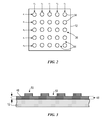
- polymeric material 32 may be deposited upon substrate 12 as a plurality of spaced-apart droplets 34 , defining a matrix array 36 .
- each droplet of droplets 34 may have a unit volume of approximately 1-10 pico-liters.
- Droplets 34 of matrix array 36 may be arranged in five columns c 1 -c 5 and five rows r 1 -r 5 .
- droplets 34 may be arranged in any two-dimensional arrangement on substrate 12 .
- An exemplary composition for polymeric material 32 is silicon-free and consists of the following:
- COMPOSITION 1 may be described in U.S. Pat. No. 7,122,079 entitled “Composition for an Etching Mask Comprising a Silicon-Containing Material”, which is incorporated by reference herein.
- polymeric material 32 may include, as an additive, a surfactant.
- a surfactant is defined as any molecule, one tail of which is hydrophobic.
- Surfactants may be either fluorine containing, e.g., include a fluorine chain, or may not include any fluorine in the surfactant molecule structure.
- An exemplary surfactant is available under the trade name ZONYL® FSO-100 from DUPONTTM that has a general structure of R 1 R 2 where R 1 ⁇ F(CF 2 CF 2 ) Y , with y being in a range of 1 to 7, inclusive and R 2 ⁇ CH 2 CH 2 O(CH 2 CH 2 O) X H, where X is in a range of 0 to 15, inclusive.
- This provides polymeric material 24 with the following composition:
- exemplary compositions from which to form polymeric material 32 are as follows:
- COMPOSITIONS 2-4 may also be described in U.S. Pat. No. 7,122,079 entitled “Composition for an Etching Mask Comprising a Silicon-Containing Material”.
- system 10 further comprises a source 38 of energy 40 coupled to direct energy 40 along a path 42 .
- Imprint head 26 and stage 14 are configured to arrange mold 18 and substrate 12 , respectively, to be in superimposition and disposed in path 42 . Either imprint head 26 , stage 14 , or both vary a distance between mold 18 and substrate 12 to define a desired volume therebetween that is filled by polymeric material 32 .
- polymeric material 32 is disposed upon substrate 12 before the desired volume is defined between mold 18 and substrate 12 .
- polymeric material 32 may fill the volume after the desired volume has been obtained.
- source 38 produces energy 40 , e.g., broadband ultraviolet radiation that causes polymeric material 32 to solidify and/or cross-link conforming to the shape of a surface 44 of substrate 12 and patterning surface 20 , defining a patterned layer 46 on substrate 12 .
- energy 40 may have a wavelength in a range of approximately 240-420 nm.
- Patterned layer 46 may comprise a residual layer 48 and a plurality of features shown as protrusions 50 and recessions 52 . Control of this process is regulated by a processor 54 that is in data communication with stage 14 , imprint head 26 , fluid dispense system 30 , and source 38 , operating on a computer readable program stored in memory 56 .
- template chuck 28 is adapted to retain template 16 upon which mold 18 is attached employing vacuum techniques.
- template chuck 28 comprises a substantially circular shape.
- template chuck 28 may comprise any geometric shape desired.
- Template chuck 28 includes first 58 and second 60 opposed sides. A side, or edge, surface 62 extends between first side 58 and second side 60 .
- First side 58 includes a first recess 64 and a second recess 66 , spaced-apart from first recess 64 , defining first 68 and second 70 spaced-apart support regions.
- First support region 68 cinctures second support region 70 and first 64 and second 66 recesses.
- Second support region 70 cinctures second recess 66 .
- first and second support regions 68 and 70 may be formed from a compliant material.
- a portion 72 of template chuck 28 in superimposition with second recess 66 may be transparent to radiation having a predetermined wavelength, such as the wavelength of the actinic radiation mentioned above.
- portion 72 may be made from a thin layer of transparent material, such as glass. However, the material from which portion 72 is made may depend upon the wavelength of radiation produced by source 38 , shown in FIG. 1 .
- Portion 72 extends between second side 60 and terminates proximate to second recess 66 and should define an area at least as large as an area of mold 18 so that mold 18 is in superimposition therewith.
- template chuck 28 may comprise any number of throughways.
- Throughway 74 places first recess 64 in fluid communication with side surface 62 , however, in a further embodiment, it should be understood that throughway 74 may place first recess 64 in fluid communication with any surface of template chuck 28 .
- template chuck 28 may comprise a throughway (not shown) placing second recess 66 in fluid communication with any surface of template chuck 28 .
- throughway 74 facilitates placing first recess 64 in fluid communication with a pressure control system, such as a pump system 76 .
- pump system 76 may include on or more pumps to control the pressure proximate to first recess 64 .
- template 18 rests against first 68 and second 70 support regions, covering first 64 and second 66 recesses.
- First recess 64 and a portion 78 of template 16 in superimposition therewith define a first chamber 80 .
- Second recess 66 and a portion 81 of template 18 in superimposition therewith define a second chamber 82 .
- Pump system 76 operates to control a pressure in first chamber 80 .
- pump system 76 may control a pressure in second chamber 82 .
- Pump system 76 may be in data communication with processor 54 , operating on computer readable program stored in memory 56 to control pump system 76 .
- a distance between mold 18 and substrate 12 is varied such that a desired volume is defined therebetween that is filled by polymeric material 32 . Furthermore, after solidification, polymeric material 32 conforms to the shape of surface 44 of substrate 12 and patterning surface 20 , defining patterning layer 46 on substrate 12 . To that end, in a volume 84 defined between droplets 34 of matrix array 36 , there are gases present, and droplets 34 in matrix array 36 are spread over substrate 12 so as to avoid, if not prevent, trapping of gases and/or gas pockets between substrate 12 and mold 18 and within pattering layer 46 .
- the gases and/or gas pockets may be such gases including, but not limited to air, nitrogen, carbon dioxide, and helium.
- Gas and/or gas pockets between substrate 12 and mold 18 and within patterning layer 46 may result in, inter alia, pattern distortion of features formed in patterning layer 46 , low fidelity of features formed in patterning layer 46 , and a non-uniform thickness of residual layer 48 across patterned layer 46 , all of which are undesirable. To that end, a method and a system of minimizing, if not preventing, trapping of gas and/or gas pockets between substrate 12 and mold 18 and within patterning layer 46 are described below.
- polymeric material 32 may be positioned on substrate 12 by drop dispense, spin-coating, dip coating, chemical vapor deposition (CVD), physical vapor deposition (PVD), thin film deposition, thick film deposition, and the like.
- polymeric material 32 may be positioned on mold 18 .
- a shape of template 16 and mold 18 may be altered such that a distance d 1 defined between mold 18 and substrate 12 at a center sub-portion of mold 18 is less than a distance defined between mold 18 and substrate 12 at remaining portions of mold 18 .
- distance d 1 is less than a distance d 2 , distance d 2 being defined at an edge of mold 18 .
- the distance d 1 may be defined at any desired location of mold 18 .
- the shape of template 16 and mold 18 may be altered by controlling a pressure within first chamber 80 . More specifically, as mentioned above, pump system 76 operates to control the pressure in first chamber 80 .
- pump system 76 may create a vacuum within first chamber 80 via throughway 74 such that portion 78 of template 18 may bow away from substrate 12 and bow towards template chuck 28 .
- portion 81 of template 18 bows toward substrate 12 and away from template chuck 28 .
- the bowing of portion 81 of template 18 may be on the order of 50 ⁇ m over 100 mm.
- either imprint head 26 shown in FIG. 1 , stage 14 , or both, may vary distance d 1 , shown in FIG. 7 , such that a sub-portion of mold 18 contacts a sub-portion of droplets 34 .
- a center sub-portion of mold 18 contacts a sub-portion of droplets 34 prior to the remaining portions of mold 18 contacting the remaining droplets of droplets 34 .
- any portion of mold 18 may contact droplets 34 prior to remaining portions of mold 18 .
- mold 18 contacts all of droplets 34 associated with column c 3 , shown in FIG.
- the shape of template 16 and mold 18 may be altered such that the desired volume defined between mold 18 and substrate 12 may be filled by polymeric material 32 , as described above with respect to FIG. 1 . More specifically, the shape of template 16 and mold 18 may be altered by the combination of controlling the pressure within first chamber 80 and a force exerted by imprint head 26 , shown in FIG. 1 , and/or stage 14 upon template 16 and mold 18 as a result of contact been polymeric material 32 and mold 18 . More specifically, as mentioned above, pump system 76 operates to control the pressure in first chamber 80 .
- pump system 76 decreases a magnitude of the vacuum created within first chamber 80 via throughway 74 such that polymeric material 32 associated with subsequent subsets of droplets 34 in columns c 2 and c 4 , shown in FIG. 2 , spread to become included in contiguous fluid sheet 85 .
- the shape of template 16 and mold 18 continues to be altered such that mold 18 subsequently comes into contact with droplets 34 associated with columns c 1 and c 5 so that polymeric material 32 associated therewith spreads to become included in contiguous sheet 85 , as shown in FIG. 11 .
- interfaces 87 a and 87 b have moved towards edges 88 a and 88 c , respectively, so that there is an unimpeded path for the gases in the remaining volume 84 , shown in FIG. 9 , to travel thereto.
- the trapping of gas and/or gas pockets between substrate 12 and mold 18 and within patterning layer 46 shown in FIG. 3 , is minimized, if not prevented.
- the shape of template 16 and mold 18 may be altered concurrently with decreasing the distance d 1 , as mentioned above with respect to FIG. 8 . Furthermore, it may be desired to balance a speed at which polymeric material 32 fills the desired volume between mold 18 and substrate 12 . More specifically, if interfaces 87 a and 87 b propagate towards edges 88 a and 88 b too fast, pockets of gas may be created between mold 18 and substrate 12 , which is undesirable. To that end, in an example, the shape of template 16 and mold 18 may be altered such that polymeric material 32 fills the desired volume between mold 18 and substrate 12 at a speed of 100 mm in a few seconds.
- polymeric material 32 may be then be solidified and/or cross-linked, defining patterned layer 46 , shown in FIG. 3 .
- mold 18 may be separated from patterned layer 46 , shown in FIG. 3 .
- the shape of template 16 and mold 18 may be altered along a first direction.
- the shape of template 16 and mold 18 may be altered concurrently in first and second directions, with the second direction extending orthogonal to the first direction. More specifically, template 16 and mold 18 may be altered such that a center sub-portion of mold 18 contacts a sub-portion of droplets 34 prior to the remaining portions of mold 18 contacting the remaining droplets of droplets 34 , as described above with respect to FIG. 9 . This causes droplets 34 to spread and to produce contiguous liquid sheet 85 of polymeric material 32 , defining continuous liquid-gas interface 87 that functions to push gases in volume 84 outward radially.
- liquid sheet 85 may have a circular or circular-like expansion of liquid-gas interface 87 to push gases in volume 84 towards edges 88 a , 88 b , 88 c , and 88 d outward radially.
- shape of template 16 and mold 18 may be altered to in any direction to produce liquid sheet 85 with any geometric shape desired to facilitate pushing gases in volume 84 towards edges 88 a , 88 b , 88 c , and 88 d outward radially to minimize, if not prevent, trapping of gas and/or gas pockets between substrate 12 and mold 18 and within patterning layer 46 .
- polymeric material 32 may be positioned on substrate 12 or mold 18 .
- mold 18 and substrate 12 are positioned such that a distance d 3 is defined therebetween.
- Imprint head 26 shown in FIG. 1 , stage 14 , or both may position mold 18 and substrate 12 to obtain distance d 3 between substrate 12 and mold 18 .
- mold 18 may extend in a first plane and substrate 12 may extend in a second plane, with the first and second planes being substantially parallel.
- distance d 3 may have a magnitude in a range of 5-50 microns.
- Distance d 3 is defined such that upon altering the shape of template 16 and mold 18 , a sub-portion of mold 18 contacts a sub-portion of droplets 34 , described further below.
- the shape of template 16 and mold 18 may be altered such that a center sub-portion of mold 18 contacts a sub-portion of droplets 34 prior to the remaining portions of mold 18 contacting the remaining droplets of droplets 34 .
- any portion of mold 18 may contact droplets 34 prior to remaining portions of mold 18 .
- mold 18 contacts all of droplets 34 associated with column c 3 , shown in FIG. 2 , substantially concurrently. This causes droplets 34 to spread and to produce a contiguous liquid sheet 85 of polymeric material 32 .
- Edges 86 a and 86 b of liquid sheet 85 define liquid-gas interfaces 87 a and 87 b , respectively, that function to push gases in volume 84 toward edges 88 a , 88 b , 88 c , and 88 d .
- Volume 84 between droplets 34 in columns c 1 -c 5 define gas passages through which gas may be pushed to edges 88 a , 88 b , 88 c , and 88 d .
- liquid-gas interfaces 87 a and 87 b in conjunction with the gas passages reduces, if not prevents, trapping of gases in liquid sheet 85 .
- the shape of template 16 and mold 18 may be further altered such that the desired volume defined between mold 18 and substrate 12 may be filled by polymeric material 32 , as described above with respect to FIG. 1 . More specifically, analogous to that mentioned above with respect to FIGS. 10-12 , the shape of template 16 and mold 18 may be altered by the combination of controlling the pressure within first chamber 80 and a force exerted by imprint head 26 and/or stage 12 upon template 16 and mold 18 as a result of contact been polymeric material 32 and mold 18 . More specifically, as mentioned above, pump system 76 operates to control the pressure in first chamber 80 .
- pump system 76 decreases a magnitude of the vacuum created within first chamber 80 via throughway 74 such that polymeric material 32 associated with subsequent subsets of droplets 34 in columns c 2 and c 4 , shown in FIG. 2 , spread to become included in contiguous fluid sheet 85 , as shown in FIG. 10 .
- the shape of template 16 and mold 18 continues to be altered such that mold 18 subsequently comes into contact with droplets 34 associated with columns c 1 and c 5 so that polymeric material 32 associated therewith spreads to become included in liquid sheet 85 , as shown in FIG. 11 .
- interfaces 87 a and 88 b have moved towards edges 88 a and 88 b , respectively, so that there is an unimpeded path for the gases in the remaining volume 84 , shown in FIG. 9 , to travel thereto.
- This allows gases in volume 84 , shown in FIG. 9 , to egress from between mold 18 and substrate 12 vis-à-vis edges 88 a , 88 b , 88 c , and 88 d .
- the trapping of gas and/or gas pockets between substrate 12 and mold 18 and within patterning layer 46 shown in FIG. 3 , is minimized, if not prevented.
- the shape of template 16 and mold 18 may be altered concurrently with decreasing the distance d 1 , as mentioned above with respect to FIG. 8 .
- polymeric material 32 may be then be solidified and/or cross-linked, defining patterned layer 46 , shown in FIG. 3 .
- mold 18 may be separated from patterned layer 46 , shown in FIG. 3 .
- substrate 12 may be subjected to the above-mentioned processes such that a shape of substrate 12 may be altered to minimize, if not prevent, trapping of gas and/or gas pockets between substrate 12 and mold 18 and within patterning layer 46 .
- template 16 , mold 18 , and substrate 12 may be subjected to the above-mentioned processes concurrently.
- template chuck 128 includes first 158 and second 160 opposed sides. A side, or edge, surface 162 extends between first side 158 and second side 160 . As shown, template chuck 128 comprises a substantially circular shape. However, in a further embodiment, template chuck 128 may comprise any geometric shape desired.
- First side 158 includes a first recess 164 and a second recess 166 , spaced-apart from first recess 164 , defining first 168 and second 170 spaced-apart support regions.
- First support region 168 cinctures second support region 170 and the first 164 and second 166 recesses.
- Second support region 170 cinctures second recess 166 .
- first and second support regions 168 and 170 may be formed from a compliant material.
- a portion 172 of template chuck 128 in superimposition with second recess 166 may be transparent to radiation having a predetermined wavelength, such as the wavelength of the actinic radiation mentioned above. To that end, portion 172 may be made from a thin layer of transparent material, such as glass. However, the material from which portion 172 is made may depend upon the wavelength of radiation production by source 38 , shown in FIG. 1 .
- Portion 172 extends between second side 160 and terminates proximate to second recess 166 and should define an area at least as large as an area of mold 18 so that mold 18 is in superimposition therewith.
- template chuck 128 further includes a plurality of pins 186 projecting from a nadir surface 188 of first recess 164 .
- Pins 186 provide mechanical support for template 16 retained on template chuck 128 via vacuum.
- Pins 186 are typically rigid posts having a circular cross-section. However, in a further embodiment, pins 186 may have any geometric shape desired.
- template chuck 128 may comprise any number of throughways.
- Throughway 174 a places first recess 164 in fluid communication with side surface 162 , however, in a further embodiment, it should be understood that throughway 174 a may place first recess 164 in fluid communication with any surface of template chuck 128 .
- Throughway 174 b places second recess 166 in fluid communication with second side 160 , however, in a further embodiment, it should be understood that throughway 174 b may place second recess 166 in fluid communication with any surface of template chuck 128 .
- throughways 174 a and 174 b facilitates placing first recess 164 and second recess 166 , respectively, in fluid communication with a pressure control system, such as a pump system 176 .
- pump system 176 may include on or more pumps to control the pressure proximate to first recess 164 and second recess 166 .
- template 16 rests against first 168 and second 170 support regions, covering first 164 and 166 recesses.
- First recess 164 and a portion 178 of template 116 in superimposition therewith define a first chamber 180 .
- Second recess 166 and a portion 181 of template 16 in superimposition therewith define a second chamber 182 .
- Pump system 176 operates to control a pressure in first and second chambers 180 and 182 .
- template chuck 128 further comprises compliant sealing 190 positioned adjacent second support region 170 to isolate first chamber 180 from second chamber 182 to facilitate obtaining a desired pressure and/or vacuum within first and second chambers 180 and 182 .
- pump system 176 may create a pressure within second chamber 182 such that portion 181 of template 18 may bow towards substrate 12 and bow away from template chuck 128 , as shown in FIG. 17 .
- Template chuck 128 may then be employed in any of the methods mentioned above with respect to minimize, if not prevent the trapping of gas and/or gas pockets between substrate 12 and mold 18 and within patterning layer 46 , shown in FIG. 3 .
- residual layer 48 in addition to minimizing, if not preventing the trapping of gas and/or gas pockets between substrate 12 and mold 18 and within patterning layer 46 , it may also be desired for residual layer 48 to be substantially uniform. More specifically, it may be desired for residual layer 48 to have a substantially uniform height h 1 defined across patterned layer 46 . To that end, to obtain residual layer 48 having a substantially uniform height hi, the desired volume defined between mold 18 and substrate 12 may be filled by capillary forces of polymeric material 32 , as described in United States patent application publication 2005/0061773, filed as U.S. patent application Ser. No. 10/645,306, now issued as U.S. Pat. No. 7,442,336 on Oct.
- each droplet of droplets 34 may spread to regions adjacent thereto in a few seconds or faster, and thus, height h 1 of residual layer may be substantially uniform over patterned layer 46 .
- a thickness t 1 of template 16 and mold 18 may further facilitate obtaining a substantially uniform height h 1 of residual layer 48 . More specifically, the thickness t 1 of template 16 and mold 18 may have a magnitude such that a bending stiffness of template 16 and mold 18 may be balanced with the aforementioned capillary forces of polymeric material 32 to facilitate obtaining a substantially uniform height h 1 of residual layer 48 . More specifically, the bending stiffness of template 16 and mold 18 is a cubic function thereof. To that end, were thickness t 1 too thick, thickness h 1 of residual layer 48 would be substantially non-uniform; however, were the thickness t 1 of template 16 and mold 18 too thin, a local defect among droplets 34 , shown in FIG.
- t 1 of template 16 and mold 18 may be in the range of 100 ⁇ m-2 mm in the presence of a few microns of out-of-plane variation in template 16 and/or substrate 12 .
- the thickness t 1 of template 16 and mold 18 may have a magnitude such that variations among height h 1 of residual layer 48 due to surface non planarity of template 16 and mold 18 are minimized, if not prevented, while having a magnitude to minimize, if not prevent, producing local undesirable variations among height h 1 of residual layer 48 due to deformations of template 16 and mold 18 resulting from fluid pressure within first and second chambers 80 and 82 , shown in FIG. 4 .
- the magnitude of thickness t 1 should also facilitate the handling of template 16 and mold 18 by system 10 and separation thereof from patterned layer 46 .
- a thickness t 2 of substrate 12 may have a magnitude in the manner described above with respect to thickness t 1 of template 16 and mold 18 .
- substrate 12 is shown comprising protrusions 192 and protrusion 194 .
- a thickness z 1 is defined between protrusion 192 and surface 196 of patterned layer 146 and a thickness z 2 is defined between protrusion 194 and surface 196 .
- thickness z 2 is greater than z 1 .
- This may result from positioning polymeric fluid 32 on substrate 12 by spin-coating, and thus, patterned layer 146 may tend to contour to the surface topology of substrate 12 , resulting in local film thickness variations among patterned layer 146 , which is undesirable.
- the methods mentioned above may be employed in planarization of polymeric fluid 32 on substrate 12 such that patterned layer 146 is substantially planar, as shown in FIG. 20 .
- the thickness z 2 is substantially the same as the thickness z 1 , which is desirable.
- protrusions 192 may be less than 200 nm wide while protrusion 194 may be on the order of 50 microns-100 microns wide.
- template 216 may be employed having a predetermined thickness such that upon contact with patterned layer 146 and/or substrate 12 , template 216 may be non-conforming thereto. To that end, as shown, template 216 has a thickness x 1 . However, thickness x 1 of template 216 facilitates template 216 conforming to patterned layer 146 in the presence of a long spatial waviness. Such a uniform layer may be used to form an etching mask to reverse the tone features, as described in United States patent application publication 2004/0188381, filed as U.S. patent application Ser. No. 10/396,615, now issued as U.S. Pat. No. 7,179,396 on Feb.
- template 216 may have a thickness x 2 , as shown in FIG. 22 , which does not conform to patterned layer 146 or substrate 12 .
- a thickness a 1 defined between a surface 198 of template 216 and surface 196 of patterned layer 146 at a first location differs from a thickness a 2 defined between surface 198 and surface 196 at a second location, differing from the first location.
- surface 196 of patterned layer 146 is substantially planar.
- thickness x 2 of template 216 may be 6.25 mm.
Abstract
Description
Claims (16)
Priority Applications (8)
| Application Number | Priority Date | Filing Date | Title |
|---|---|---|---|
| US11/565,393 US7691313B2 (en) | 2002-11-13 | 2006-11-30 | Method for expelling gas positioned between a substrate and a mold |
| US11/749,909 US7641840B2 (en) | 2002-11-13 | 2007-05-17 | Method for expelling gas positioned between a substrate and a mold |
| TW96117879A TWI322754B (en) | 2006-05-18 | 2007-05-18 | Method for expelling gas positioned between a substrate and a mold |
| PCT/US2007/012071 WO2007136832A2 (en) | 2006-05-18 | 2007-05-18 | Method for expelling gas positioned between a substrate and a mold |
| US12/026,049 US7708926B2 (en) | 2002-07-11 | 2008-02-05 | Capillary imprinting technique |
| US12/707,345 US8282383B2 (en) | 2002-11-13 | 2010-02-17 | Method for expelling gas positioned between a substrate and a mold |
| US12/707,365 US7910042B2 (en) | 2002-07-11 | 2010-02-17 | Capillary imprinting technique |
| US13/028,336 US8057725B2 (en) | 2002-07-11 | 2011-02-16 | Capillary imprinting technique |
Applications Claiming Priority (4)
| Application Number | Priority Date | Filing Date | Title |
|---|---|---|---|
| US10/293,224 US7019819B2 (en) | 2002-11-13 | 2002-11-13 | Chucking system for modulating shapes of substrates |
| US74838005P | 2005-12-08 | 2005-12-08 | |
| US11/389,731 US7224443B2 (en) | 2002-11-13 | 2006-03-27 | Imprint lithography substrate processing tool for modulating shapes of substrates |
| US11/565,393 US7691313B2 (en) | 2002-11-13 | 2006-11-30 | Method for expelling gas positioned between a substrate and a mold |
Related Parent Applications (1)
| Application Number | Title | Priority Date | Filing Date |
|---|---|---|---|
| US11/389,731 Continuation US7224443B2 (en) | 2002-07-11 | 2006-03-27 | Imprint lithography substrate processing tool for modulating shapes of substrates |
Related Child Applications (4)
| Application Number | Title | Priority Date | Filing Date |
|---|---|---|---|
| US10/194,991 Continuation US7077992B2 (en) | 2002-07-11 | 2002-07-11 | Step and repeat imprint lithography processes |
| US11/749,909 Continuation-In-Part US7641840B2 (en) | 2002-11-13 | 2007-05-17 | Method for expelling gas positioned between a substrate and a mold |
| US12/026,049 Continuation US7708926B2 (en) | 2002-07-11 | 2008-02-05 | Capillary imprinting technique |
| US12/707,345 Continuation US8282383B2 (en) | 2002-11-13 | 2010-02-17 | Method for expelling gas positioned between a substrate and a mold |
Publications (2)
| Publication Number | Publication Date |
|---|---|
| US20070114686A1 US20070114686A1 (en) | 2007-05-24 |
| US7691313B2 true US7691313B2 (en) | 2010-04-06 |
Family
ID=32229628
Family Applications (5)
| Application Number | Title | Priority Date | Filing Date |
|---|---|---|---|
| US10/293,224 Expired - Lifetime US7019819B2 (en) | 2002-07-11 | 2002-11-13 | Chucking system for modulating shapes of substrates |
| US10/864,591 Expired - Lifetime US6982783B2 (en) | 2002-11-13 | 2004-06-09 | Chucking system for modulating shapes of substrates |
| US11/389,731 Expired - Lifetime US7224443B2 (en) | 2002-07-11 | 2006-03-27 | Imprint lithography substrate processing tool for modulating shapes of substrates |
| US11/565,393 Expired - Lifetime US7691313B2 (en) | 2002-07-11 | 2006-11-30 | Method for expelling gas positioned between a substrate and a mold |
| US12/707,345 Expired - Lifetime US8282383B2 (en) | 2002-11-13 | 2010-02-17 | Method for expelling gas positioned between a substrate and a mold |
Family Applications Before (3)
| Application Number | Title | Priority Date | Filing Date |
|---|---|---|---|
| US10/293,224 Expired - Lifetime US7019819B2 (en) | 2002-07-11 | 2002-11-13 | Chucking system for modulating shapes of substrates |
| US10/864,591 Expired - Lifetime US6982783B2 (en) | 2002-11-13 | 2004-06-09 | Chucking system for modulating shapes of substrates |
| US11/389,731 Expired - Lifetime US7224443B2 (en) | 2002-07-11 | 2006-03-27 | Imprint lithography substrate processing tool for modulating shapes of substrates |
Family Applications After (1)
| Application Number | Title | Priority Date | Filing Date |
|---|---|---|---|
| US12/707,345 Expired - Lifetime US8282383B2 (en) | 2002-11-13 | 2010-02-17 | Method for expelling gas positioned between a substrate and a mold |
Country Status (2)
| Country | Link |
|---|---|
| US (5) | US7019819B2 (en) |
| CN (1) | CN1726429B (en) |
Cited By (22)
| Publication number | Priority date | Publication date | Assignee | Title |
|---|---|---|---|---|
| US20050270312A1 (en) * | 2004-06-03 | 2005-12-08 | Molecular Imprints, Inc. | Fluid dispensing and drop-on-demand dispensing for nano-scale manufacturing |
| US20080202365A1 (en) * | 2005-05-03 | 2008-08-28 | Koninklijke Philips Electronics, N.V. | Method and Device For Transferring a Pattern From a Stamp to a Substrate |
| US20090053350A1 (en) * | 2007-08-24 | 2009-02-26 | Delta Pt, Llc | Pressure compensating molding system |
| US20090148619A1 (en) * | 2007-12-05 | 2009-06-11 | Molecular Imprints, Inc. | Controlling Thickness of Residual Layer |
| US20100083855A1 (en) * | 2006-12-04 | 2010-04-08 | Koninklijke Philips Electronics N.V. | Method and apparatus for applying a sheet to a substrate |
| US20100096774A1 (en) * | 2008-10-17 | 2010-04-22 | Asml Netherlands B.V. | Imprint lithography apparatus and method |
| US20100096764A1 (en) * | 2008-10-20 | 2010-04-22 | Molecular Imprints, Inc. | Gas Environment for Imprint Lithography |
| US20100102469A1 (en) * | 2008-10-24 | 2010-04-29 | Molecular Imprints, Inc. | Strain and Kinetics Control During Separation Phase of Imprint Process |
| US20100112220A1 (en) * | 2008-11-03 | 2010-05-06 | Molecular Imprints, Inc. | Dispense system set-up and characterization |
| US20100237042A1 (en) * | 2009-03-23 | 2010-09-23 | Intevac, Inc. | Process for optimization of island to trench ratio in patterned media |
| US20110084417A1 (en) * | 2009-10-08 | 2011-04-14 | Molecular Imprints, Inc. | Large area linear array nanoimprinting |
| US20110171340A1 (en) * | 2002-07-08 | 2011-07-14 | Molecular Imprints, Inc. | Template Having a Varying Thickness to Facilitate Expelling a Gas Positioned Between a Substrate and the Template |
| US20130056905A1 (en) * | 2011-09-07 | 2013-03-07 | Canon Kabushiki Kaisha | Imprint apparatus and article manufacturing method using same |
| US20130056904A1 (en) * | 2011-09-07 | 2013-03-07 | Canon Kabushiki Kaisha | Imprint apparatus and article manufacturing method using same |
| US20130181365A1 (en) * | 2012-01-16 | 2013-07-18 | Canon Kabushiki Kaisha | Imprint apparatus and article manufacturing method |
| WO2013126750A1 (en) | 2012-02-22 | 2013-08-29 | Molecular Imprints, Inc. | Large area imprint lithography |
| US20130292865A1 (en) * | 2012-05-03 | 2013-11-07 | Samsung Electronics Co., Ltd. | Template system and nano-imprint method using the same |
| US20140367875A1 (en) * | 2012-02-07 | 2014-12-18 | Canon Kabushiki Kaisha | Imprint apparatus and method of manufacturing article |
| US20150137332A1 (en) * | 2012-11-15 | 2015-05-21 | Industrial Technology Research Institute | Carrier for a semiconductor layer |
| US20150190961A1 (en) * | 2014-01-08 | 2015-07-09 | Canon Kabushiki Kaisha | Imprint apparatus, imprint method, and method of manufacturing article |
| US20180056577A1 (en) * | 2016-08-25 | 2018-03-01 | National Cheng Kung University | Flexible mold with variable thickness |
| US11590687B2 (en) | 2020-06-30 | 2023-02-28 | Canon Kabushiki Kaisha | Systems and methods for reducing pressure while shaping a film |
Families Citing this family (97)
| Publication number | Priority date | Publication date | Assignee | Title |
|---|---|---|---|---|
| EP1303792B1 (en) * | 2000-07-16 | 2012-10-03 | Board Of Regents, The University Of Texas System | High-resolution overlay alignement methods and systems for imprint lithography |
| US8016277B2 (en) * | 2000-08-21 | 2011-09-13 | Board Of Regents, The University Of Texas System | Flexure based macro motion translation stage |
| US20050274219A1 (en) | 2004-06-01 | 2005-12-15 | Molecular Imprints, Inc. | Method and system to control movement of a body for nano-scale manufacturing |
| JP2004523906A (en) * | 2000-10-12 | 2004-08-05 | ボード・オブ・リージエンツ,ザ・ユニバーシテイ・オブ・テキサス・システム | Templates for room-temperature and low-pressure micro and nano-transfer lithography |
| US7037639B2 (en) * | 2002-05-01 | 2006-05-02 | Molecular Imprints, Inc. | Methods of manufacturing a lithography template |
| US7442336B2 (en) * | 2003-08-21 | 2008-10-28 | Molecular Imprints, Inc. | Capillary imprinting technique |
| US7019819B2 (en) * | 2002-11-13 | 2006-03-28 | Molecular Imprints, Inc. | Chucking system for modulating shapes of substrates |
| US7077992B2 (en) * | 2002-07-11 | 2006-07-18 | Molecular Imprints, Inc. | Step and repeat imprint lithography processes |
| US8349241B2 (en) | 2002-10-04 | 2013-01-08 | Molecular Imprints, Inc. | Method to arrange features on a substrate to replicate features having minimal dimensional variability |
| US7641840B2 (en) * | 2002-11-13 | 2010-01-05 | Molecular Imprints, Inc. | Method for expelling gas positioned between a substrate and a mold |
| US6871558B2 (en) * | 2002-12-12 | 2005-03-29 | Molecular Imprints, Inc. | Method for determining characteristics of substrate employing fluid geometries |
| TW200500811A (en) * | 2002-12-13 | 2005-01-01 | Molecular Imprints Inc | Magnification correction employing out-of-plane distortion of a substrate |
| US7452574B2 (en) * | 2003-02-27 | 2008-11-18 | Molecular Imprints, Inc. | Method to reduce adhesion between a polymerizable layer and a substrate employing a fluorine-containing layer |
| JP4340086B2 (en) * | 2003-03-20 | 2009-10-07 | 株式会社日立製作所 | Nanoprinting stamper and fine structure transfer method |
| US6829988B2 (en) * | 2003-05-16 | 2004-12-14 | Suss Microtec, Inc. | Nanoimprinting apparatus and method |
| US7090716B2 (en) * | 2003-10-02 | 2006-08-15 | Molecular Imprints, Inc. | Single phase fluid imprint lithography method |
| US8211214B2 (en) * | 2003-10-02 | 2012-07-03 | Molecular Imprints, Inc. | Single phase fluid imprint lithography method |
| US8076386B2 (en) | 2004-02-23 | 2011-12-13 | Molecular Imprints, Inc. | Materials for imprint lithography |
| WO2005119802A2 (en) * | 2004-05-28 | 2005-12-15 | Board Of Regents, The University Of Texas System | Adaptive shape substrate support system and method |
| US20050270516A1 (en) * | 2004-06-03 | 2005-12-08 | Molecular Imprints, Inc. | System for magnification and distortion correction during nano-scale manufacturing |
| US7785526B2 (en) | 2004-07-20 | 2010-08-31 | Molecular Imprints, Inc. | Imprint alignment method, system, and template |
| US7309225B2 (en) * | 2004-08-13 | 2007-12-18 | Molecular Imprints, Inc. | Moat system for an imprint lithography template |
| US20060062922A1 (en) | 2004-09-23 | 2006-03-23 | Molecular Imprints, Inc. | Polymerization technique to attenuate oxygen inhibition of solidification of liquids and composition therefor |
| US20060145398A1 (en) * | 2004-12-30 | 2006-07-06 | Board Of Regents, The University Of Texas System | Release layer comprising diamond-like carbon (DLC) or doped DLC with tunable composition for imprint lithography templates and contact masks |
| US7798801B2 (en) * | 2005-01-31 | 2010-09-21 | Molecular Imprints, Inc. | Chucking system for nano-manufacturing |
| US7636999B2 (en) * | 2005-01-31 | 2009-12-29 | Molecular Imprints, Inc. | Method of retaining a substrate to a wafer chuck |
| US7635263B2 (en) * | 2005-01-31 | 2009-12-22 | Molecular Imprints, Inc. | Chucking system comprising an array of fluid chambers |
| US7670534B2 (en) | 2005-09-21 | 2010-03-02 | Molecular Imprints, Inc. | Method to control an atmosphere between a body and a substrate |
| US7906058B2 (en) * | 2005-12-01 | 2011-03-15 | Molecular Imprints, Inc. | Bifurcated contact printing technique |
| ATE510241T1 (en) * | 2005-12-08 | 2011-06-15 | Molecular Imprints Inc | METHOD FOR EXPECTING GAS BETWEEN A SUBSTRATE AND A MOLD |
| US7670530B2 (en) | 2006-01-20 | 2010-03-02 | Molecular Imprints, Inc. | Patterning substrates employing multiple chucks |
| MY144847A (en) * | 2005-12-08 | 2011-11-30 | Molecular Imprints Inc | Method and system for double-sided patterning of substrates |
| US20070200276A1 (en) * | 2006-02-24 | 2007-08-30 | Micron Technology, Inc. | Method for rapid printing of near-field and imprint lithographic features |
| US20070231422A1 (en) * | 2006-04-03 | 2007-10-04 | Molecular Imprints, Inc. | System to vary dimensions of a thin template |
| ATE513625T1 (en) * | 2006-04-03 | 2011-07-15 | Molecular Imprints Inc | LITHOGRAPH PRINTING SYSTEM |
| US7936447B2 (en) * | 2006-05-08 | 2011-05-03 | Asml Netherlands B.V. | Lithographic apparatus and device manufacturing method |
| US8215946B2 (en) | 2006-05-18 | 2012-07-10 | Molecular Imprints, Inc. | Imprint lithography system and method |
| DE102006024524A1 (en) * | 2006-05-23 | 2007-12-06 | Von Ardenne Anlagentechnik Gmbh | Transparent multi-layer composite system capable of reflecting infrared radiation for hardening and/or shaping of substrates and temperature process, comprises layers, anti-reflection coating, blocking layer and dielectric interface layer |
| WO2008082650A1 (en) * | 2006-12-29 | 2008-07-10 | Molecular Imprints, Inc. | Imprint fluid control |
| GB2445573B (en) * | 2007-01-10 | 2009-08-26 | Vistec Lithography Ltd | Apparatus support structure |
| JP5041214B2 (en) | 2007-06-15 | 2012-10-03 | ソニー株式会社 | Method for forming metal thin film and method for manufacturing electronic device |
| US20090014917A1 (en) * | 2007-07-10 | 2009-01-15 | Molecular Imprints, Inc. | Drop Pattern Generation for Imprint Lithography |
| CN101808808B (en) | 2007-09-28 | 2013-05-01 | 东丽株式会社 | Method and device for manufacturing sheet having fine shape transferred thereon |
| US8119052B2 (en) * | 2007-11-02 | 2012-02-21 | Molecular Imprints, Inc. | Drop pattern generation for imprint lithography |
| US8945444B2 (en) * | 2007-12-04 | 2015-02-03 | Canon Nanotechnologies, Inc. | High throughput imprint based on contact line motion tracking control |
| US8361371B2 (en) * | 2008-02-08 | 2013-01-29 | Molecular Imprints, Inc. | Extrusion reduction in imprint lithography |
| JP4482047B2 (en) * | 2008-03-28 | 2010-06-16 | 株式会社東芝 | Imprint method |
| WO2009129441A2 (en) * | 2008-04-17 | 2009-10-22 | Massachusetts Institute Of Technology | Symmetric thermocentric flexure with minimal yaw error motion |
| US20100015270A1 (en) * | 2008-07-15 | 2010-01-21 | Molecular Imprints, Inc. | Inner cavity system for nano-imprint lithography |
| IT1390890B1 (en) * | 2008-07-18 | 2011-10-19 | S I P A Societa' Ind Progettazione E Automazione S P A | CONVEYING PLANT FOR CONTAINERS IN PLASTIC MATERIAL |
| KR101004769B1 (en) * | 2008-09-09 | 2011-01-04 | 서울대학교산학협력단 | Optofluidic Lithography System and a Manufacturing Method of Three-Dimensional Microstructures |
| US20100096470A1 (en) * | 2008-10-17 | 2010-04-22 | Molecular Imprints, Inc. | Drop volume reduction |
| US20100098858A1 (en) * | 2008-10-17 | 2010-04-22 | Molecular Imprints, Inc. | Fluid Dispense System Coating |
| US8586126B2 (en) | 2008-10-21 | 2013-11-19 | Molecular Imprints, Inc. | Robust optimization to generate drop patterns in imprint lithography which are tolerant of variations in drop volume and drop placement |
| US8512797B2 (en) * | 2008-10-21 | 2013-08-20 | Molecular Imprints, Inc. | Drop pattern generation with edge weighting |
| JP4940262B2 (en) * | 2009-03-25 | 2012-05-30 | 株式会社東芝 | Imprint pattern forming method |
| JP5411557B2 (en) * | 2009-04-03 | 2014-02-12 | 株式会社日立ハイテクノロジーズ | Microstructure transfer device |
| JP2010266475A (en) * | 2009-05-12 | 2010-11-25 | Nitto Denko Corp | Method for manufacturing optical waveguide |
| US9164375B2 (en) * | 2009-06-19 | 2015-10-20 | Canon Nanotechnologies, Inc. | Dual zone template chuck |
| JP5443070B2 (en) * | 2009-06-19 | 2014-03-19 | 東京エレクトロン株式会社 | Imprint system |
| JP5060517B2 (en) * | 2009-06-24 | 2012-10-31 | 東京エレクトロン株式会社 | Imprint system |
| JP2011009641A (en) * | 2009-06-29 | 2011-01-13 | Toshiba Corp | Method of manufacturing semiconductor device, and template for imprint |
| US8913230B2 (en) * | 2009-07-02 | 2014-12-16 | Canon Nanotechnologies, Inc. | Chucking system with recessed support feature |
| JP2011071500A (en) * | 2009-08-31 | 2011-04-07 | Fujifilm Corp | Pattern transfer apparatus and pattern forming method |
| EP2496989B1 (en) * | 2009-11-02 | 2013-10-02 | Danmarks Tekniske Universitet | Method and device for nanoimprint lithography |
| US8747092B2 (en) * | 2010-01-22 | 2014-06-10 | Nanonex Corporation | Fast nanoimprinting apparatus using deformale mold |
| US20110180964A1 (en) * | 2010-01-27 | 2011-07-28 | Molecular Imprints. Inc. | Systems and methods for substrate formation |
| US8691134B2 (en) * | 2010-01-28 | 2014-04-08 | Molecular Imprints, Inc. | Roll-to-roll imprint lithography and purging system |
| WO2011139782A1 (en) | 2010-04-27 | 2011-11-10 | Molecular Imprints, Inc. | Separation control substrate/template for nanoimprint lithography |
| JP5828626B2 (en) * | 2010-10-04 | 2015-12-09 | キヤノン株式会社 | Imprint method |
| JP5930622B2 (en) | 2010-10-08 | 2016-06-08 | キヤノン株式会社 | Imprint apparatus and article manufacturing method |
| JP2013021155A (en) * | 2011-07-12 | 2013-01-31 | Canon Inc | Imprint apparatus and method of manufacturing product using the same |
| JP5787691B2 (en) * | 2011-09-21 | 2015-09-30 | キヤノン株式会社 | Imprint apparatus and article manufacturing method using the same |
| WO2013044181A1 (en) * | 2011-09-23 | 2013-03-28 | 1366 Technologies Inc. | Methods and apparati for handling, heating and cooling a substrate upon which a pattern is made by a tool in heat flowable material coating, including substrate transport, tool laydown, tool tensioning, and tool retraction |
| US10108086B2 (en) | 2013-03-15 | 2018-10-23 | Nanonex Corporation | System and methods of mold/substrate separation for imprint lithography |
| US10105883B2 (en) | 2013-03-15 | 2018-10-23 | Nanonex Corporation | Imprint lithography system and method for manufacturing |
| EP3066524A1 (en) | 2013-11-08 | 2016-09-14 | Canon Nanotechnologies, Inc. | Low contact imprint lithography template chuck system for improved overlay correction |
| US10409156B2 (en) * | 2015-02-13 | 2019-09-10 | Canon Kabushiki Kaisha | Mold, imprint apparatus, and method of manufacturing article |
| JP2016157784A (en) * | 2015-02-24 | 2016-09-01 | 株式会社東芝 | Pattern forming method and pattern forming apparatus |
| US10024654B2 (en) | 2015-04-06 | 2018-07-17 | Kla-Tencor Corporation | Method and system for determining in-plane distortions in a substrate |
| JP6774178B2 (en) * | 2015-11-16 | 2020-10-21 | キヤノン株式会社 | Equipment for processing substrates and manufacturing methods for articles |
| NL2016593B1 (en) * | 2016-04-12 | 2017-11-01 | Iai Ind Systems B V | Method and apparatus for applying a layer having a relief on a flat face of a substrate. |
| JP2016149578A (en) * | 2016-05-11 | 2016-08-18 | 大日本印刷株式会社 | Production method of replica template for nanoimprinting |
| JP7041121B2 (en) | 2016-08-03 | 2022-03-23 | ボード オブ リージェンツ,ザ ユニバーシティ オブ テキサス システム | Wafer-scale programmable membrane for semiconductor flattening and imprint lithography |
| CN106094429B (en) * | 2016-08-19 | 2019-11-05 | 京东方科技集团股份有限公司 | Imprinting apparatus and its working method |
| JP6762853B2 (en) | 2016-11-11 | 2020-09-30 | キヤノン株式会社 | Equipment, methods, and article manufacturing methods |
| US11454883B2 (en) * | 2016-11-14 | 2022-09-27 | Canon Kabushiki Kaisha | Template replication |
| JP6940944B2 (en) | 2016-12-06 | 2021-09-29 | キヤノン株式会社 | Imprint device and article manufacturing method |
| US10578984B2 (en) | 2016-12-20 | 2020-03-03 | Canon Kabushiki Kaisha | Adaptive chucking system |
| US10895806B2 (en) * | 2017-09-29 | 2021-01-19 | Canon Kabushiki Kaisha | Imprinting method and apparatus |
| EP3707747A4 (en) | 2017-11-10 | 2021-07-28 | Applied Materials, Inc. | Patterned chuck for double-sided processing |
| KR102455415B1 (en) * | 2017-12-18 | 2022-10-17 | 삼성전자주식회사 | Substrate bonding apparatus and method of bonding a pair of substrates using the same |
| US20190259648A1 (en) | 2018-02-20 | 2019-08-22 | Applied Materials, Inc. | Patterned vacuum chuck for double-sided processing |
| JP7022615B2 (en) * | 2018-02-26 | 2022-02-18 | キヤノン株式会社 | Imprint method, imprint device, mold manufacturing method, and article manufacturing method |
| JP7134055B2 (en) | 2018-10-09 | 2022-09-09 | キヤノン株式会社 | Molding apparatus and article manufacturing method |
| US11562924B2 (en) * | 2020-01-31 | 2023-01-24 | Canon Kabushiki Kaisha | Planarization apparatus, planarization process, and method of manufacturing an article |
| US11728203B2 (en) * | 2020-10-13 | 2023-08-15 | Canon Kabushiki Kaisha | Chuck assembly, planarization process, apparatus and method of manufacturing an article |
Citations (173)
| Publication number | Priority date | Publication date | Assignee | Title |
|---|---|---|---|---|
| US3637381A (en) * | 1966-09-22 | 1972-01-25 | Teeg Research Inc | Radiation-sensitive self-revealing elements and methods of making and utilizing the same |
| US3997447A (en) | 1974-06-07 | 1976-12-14 | Composite Sciences, Inc. | Fluid processing apparatus |
| US4119688A (en) * | 1975-11-03 | 1978-10-10 | International Business Machines Corporation | Electro-lithography method |
| US4223261A (en) | 1978-08-23 | 1980-09-16 | Exxon Research & Engineering Co. | Multi-phase synchronous machine system |
| US4279628A (en) | 1979-12-31 | 1981-07-21 | Energy Synergistics, Inc. | Apparatus for drying a natural gas stream |
| US4312823A (en) * | 1977-03-14 | 1982-01-26 | U.S. Philips Corporation | Method of manufacturing a plastic record carrier having a stratified structure |
| US4395211A (en) * | 1979-08-10 | 1983-07-26 | U.S. Philips Corporation | Method and device for manufacturing a plastic record carrier |
| US4475223A (en) * | 1981-06-12 | 1984-10-02 | Hitachi, Ltd. | Exposure process and system |
| US4506184A (en) * | 1984-01-10 | 1985-03-19 | Varian Associates, Inc. | Deformable chuck driven by piezoelectric means |
| US4512848A (en) | 1984-02-06 | 1985-04-23 | Exxon Research And Engineering Co. | Procedure for fabrication of microstructures over large areas using physical replication |
| US4521175A (en) | 1980-03-14 | 1985-06-04 | Multivac Sepp Haggenmuller Kg | Apparatus for producing containers from thermoplastic sheet material |
| US4551192A (en) * | 1983-06-30 | 1985-11-05 | International Business Machines Corporation | Electrostatic or vacuum pinchuck formed with microcircuit lithography |
| US4559717A (en) | 1984-02-21 | 1985-12-24 | The United States Of America As Represented By The Secretary Of Commerce | Flexure hinge |
| US4689004A (en) | 1985-04-18 | 1987-08-25 | Firma Carl Freudenberg | Apparatus for adhering thermally-softenable plastic particles into a plastic body |
| US4724222A (en) * | 1986-04-28 | 1988-02-09 | American Telephone And Telegraph Company, At&T Bell Laboratories | Wafer chuck comprising a curved reference surface |
| US4731155A (en) | 1987-04-15 | 1988-03-15 | General Electric Company | Process for forming a lithographic mask |
| US4767584A (en) | 1985-04-03 | 1988-08-30 | Massachusetts Institute Of Technology | Process of and apparatus for producing design patterns in materials |
| US4887282A (en) * | 1986-11-18 | 1989-12-12 | Siemens Aktiengesellschaft | Method and apparatus for changing the imaging scale in X-ray lithograph |
| US5028361A (en) | 1987-11-09 | 1991-07-02 | Takeo Fujimoto | Method for molding a photosensitive composition |
| US5028366A (en) | 1988-01-12 | 1991-07-02 | Air Products And Chemicals, Inc. | Water based mold release compositions for making molded polyurethane foam |
| US5132069A (en) | 1987-07-10 | 1992-07-21 | Newton John R | Method of injection molding composite articles |
| US5213600A (en) * | 1987-06-09 | 1993-05-25 | International Business Machines Corp. | Method of manufacturing an optical storage disk |
| US5259926A (en) | 1991-09-24 | 1993-11-09 | Hitachi, Ltd. | Method of manufacturing a thin-film pattern on a substrate |
| US5324012A (en) | 1991-07-16 | 1994-06-28 | Nikon Corporation | Holding apparatus for holding an article such as a semiconductor wafer |
| US5331371A (en) | 1990-09-26 | 1994-07-19 | Canon Kabushiki Kaisha | Alignment and exposure method |
| US5338177A (en) | 1992-04-22 | 1994-08-16 | Societe Nationale Industrielle Et Aerospatiale | Hot compacting device for the production of parts requiring simultaneous pressure and temperature rises |
| US5364222A (en) * | 1992-02-05 | 1994-11-15 | Tokyo Electron Limited | Apparatus for processing wafer-shaped substrates |
| US5425848A (en) | 1993-03-16 | 1995-06-20 | U.S. Philips Corporation | Method of providing a patterned relief of cured photoresist on a flat substrate surface and device for carrying out such a method |
| US5512131A (en) | 1993-10-04 | 1996-04-30 | President And Fellows Of Harvard College | Formation of microstamped patterns on surfaces and derivative articles |
| US5515167A (en) | 1994-09-13 | 1996-05-07 | Hughes Aircraft Company | Transparent optical chuck incorporating optical monitoring |
| US5527662A (en) * | 1990-05-24 | 1996-06-18 | Matsushita Electric Industrial Co., Ltd. | Process for forming fine pattern |
| US5534073A (en) * | 1992-09-07 | 1996-07-09 | Mitsubishi Denki Kabushiki Kaisha | Semiconductor producing apparatus comprising wafer vacuum chucking device |
| US5545367A (en) | 1992-04-15 | 1996-08-13 | Soane Technologies, Inc. | Rapid prototype three dimensional stereolithography |
| US5550654A (en) * | 1993-07-19 | 1996-08-27 | Lucent Technologies Inc. | Method for forming, in optical media, refractive index perturbations having reduced birefringence |
| US5563684A (en) | 1994-11-30 | 1996-10-08 | Sgs-Thomson Microelectronics, Inc. | Adaptive wafer modulator for placing a selected pattern on a semiconductor wafer |
| US5601641A (en) | 1992-07-21 | 1997-02-11 | Tse Industries, Inc. | Mold release composition with polybutadiene and method of coating a mold core |
| US5669303A (en) * | 1996-03-04 | 1997-09-23 | Motorola | Apparatus and method for stamping a surface |
| US5772905A (en) | 1995-11-15 | 1998-06-30 | Regents Of The University Of Minnesota | Nanoimprint lithography |
| US5776748A (en) | 1993-10-04 | 1998-07-07 | President And Fellows Of Harvard College | Method of formation of microstamped patterns on plates for adhesion of cells and other biological materials, devices and uses therefor |
| US5804089A (en) * | 1994-10-31 | 1998-09-08 | Matsushita Electric Industrial Co., Ltd. | Plasma processing apparatus and method |
| US5821175A (en) | 1988-07-08 | 1998-10-13 | Cauldron Limited Partnership | Removal of surface contaminants by irradiation using various methods to achieve desired inert gas flow over treated surface |
| US5820769A (en) | 1995-05-24 | 1998-10-13 | Regents Of The University Of Minnesota | Method for making magnetic storage having discrete elements with quantized magnetic moments |
| US5849209A (en) | 1995-03-31 | 1998-12-15 | Johnson & Johnson Vision Products, Inc. | Mold material made with additives |
| US5849222A (en) | 1995-09-29 | 1998-12-15 | Johnson & Johnson Vision Products, Inc. | Method for reducing lens hole defects in production of contact lens blanks |
| US5923408A (en) | 1996-01-31 | 1999-07-13 | Canon Kabushiki Kaisha | Substrate holding system and exposure apparatus using the same |
| US5948470A (en) | 1997-04-28 | 1999-09-07 | Harrison; Christopher | Method of nanoscale patterning and products made thereby |
| US5947027A (en) * | 1998-09-08 | 1999-09-07 | Motorola, Inc. | Printing apparatus with inflatable means for advancing a substrate towards the stamping surface |
| US5997963A (en) | 1998-05-05 | 1999-12-07 | Ultratech Stepper, Inc. | Microchamber |
| US6019166A (en) | 1997-12-30 | 2000-02-01 | Intel Corporation | Pickup chuck with an integral heatsink |
| US6030275A (en) * | 1998-03-17 | 2000-02-29 | International Business Machines Corporation | Variable control of carrier curvature with direct feedback loop |
| US6032506A (en) * | 1996-05-30 | 2000-03-07 | S.C. Recherche Et Developpement Groupe | Improvment to the blank holder force regulating system in a press |
| US6099771A (en) | 1998-07-08 | 2000-08-08 | Lear Corporation | Vacuum compression method for forming molded thermoplastic floor mat having a "Class A" finish |
| US6137562A (en) * | 1996-12-05 | 2000-10-24 | Nikon Corporation | Substrate adjuster, substrate holder and substrate holding method |
| US6160430A (en) | 1999-03-22 | 2000-12-12 | Ati International Srl | Powerup sequence artificial voltage supply circuit |
| US6159400A (en) | 1995-08-01 | 2000-12-12 | Laquer; Henry Louis | Method for deforming solids in a controlled atmosphere and at adjustable rates, pressures and temperature |
| EP1072954A2 (en) | 1999-07-28 | 2001-01-31 | Lucent Technologies Inc. | Lithographic process for device fabrication |
| US6182510B1 (en) | 1997-04-30 | 2001-02-06 | Sensys Instruments Corporation | Apparatus and method for characterizing semiconductor wafers during processing |
| US6218316B1 (en) | 1998-10-22 | 2001-04-17 | Micron Technology, Inc. | Planarization of non-planar surfaces in device fabrication |
| US6220561B1 (en) | 1999-06-30 | 2001-04-24 | Sandia Corporation | Compound floating pivot micromechanisms |
| WO2001040875A1 (en) | 1999-11-30 | 2001-06-07 | Silicon Valley Group, Inc. | Dual-stage lithography apparatus and method |
| US6247579B1 (en) | 1999-01-18 | 2001-06-19 | Tokyo Ohka Kogyo Co., Ltd | Substrate transfer apparatus and method of substrate transfer |
| US6257866B1 (en) | 1996-06-18 | 2001-07-10 | Hy-Tech Forming Systems, Inc. | Apparatus for accurately forming plastic sheet |
| US6305677B1 (en) | 1999-03-30 | 2001-10-23 | Lam Research Corporation | Perimeter wafer lifting |
| US6309580B1 (en) | 1995-11-15 | 2001-10-30 | Regents Of The University Of Minnesota | Release surfaces, particularly for use in nanoimprint lithography |
| US6313567B1 (en) | 2000-04-10 | 2001-11-06 | Motorola, Inc. | Lithography chuck having piezoelectric elements, and method |
| US6334960B1 (en) | 1999-03-11 | 2002-01-01 | Board Of Regents, The University Of Texas System | Step and flash imprint lithography |
| US20020018190A1 (en) | 2000-06-15 | 2002-02-14 | Hideki Nogawa | Exposure apparatus and device manufacturing method |
| US6355198B1 (en) | 1996-03-15 | 2002-03-12 | President And Fellows Of Harvard College | Method of forming articles including waveguides via capillary micromolding and microtransfer molding |
| US20020042027A1 (en) | 1998-10-09 | 2002-04-11 | Chou Stephen Y. | Microscale patterning and articles formed thereby |
| US6383890B2 (en) * | 1997-12-26 | 2002-05-07 | Canon Kabushiki Kaisha | Wafer bonding method, apparatus and vacuum chuck |
| US6391217B2 (en) | 1999-12-23 | 2002-05-21 | University Of Massachusetts | Methods and apparatus for forming submicron patterns on films |
| US20020069525A1 (en) | 2000-09-18 | 2002-06-13 | Junichi Hada | Apparatus and method for mounting components on substrate |
| US6407006B1 (en) | 1999-09-09 | 2002-06-18 | Honeywell International, Inc. | Method for integrated circuit planarization |
| US6416311B1 (en) | 1998-05-04 | 2002-07-09 | Jenoptik Aktiengesellschaft | Device and method for separating a shaped substrate from a stamping tool |
| US20020094496A1 (en) * | 2000-07-17 | 2002-07-18 | Choi Byung J. | Method and system of automatic fluid dispensing for imprint lithography processes |
| US20020132482A1 (en) | 2000-07-18 | 2002-09-19 | Chou Stephen Y. | Fluid pressure imprint lithography |
| US6461524B1 (en) | 1999-05-27 | 2002-10-08 | Sanyo Electric Co., Ltd. | Method of filtering a fluid |
| US20020150398A1 (en) | 2000-08-21 | 2002-10-17 | Choi Byung J. | Flexure based macro motion translation stage |
| US6512401B2 (en) | 1999-09-10 | 2003-01-28 | Intel Corporation | Output buffer for high and low voltage bus |
| US6518189B1 (en) | 1995-11-15 | 2003-02-11 | Regents Of The University Of Minnesota | Method and apparatus for high density nanostructures |
| US6517995B1 (en) | 1999-09-14 | 2003-02-11 | Massachusetts Institute Of Technology | Fabrication of finely featured devices by liquid embossing |
| US20030062334A1 (en) | 2001-09-25 | 2003-04-03 | Lee Hong Hie | Method for forming a micro-pattern on a substrate by using capillary force |
| US20030080472A1 (en) | 2001-10-29 | 2003-05-01 | Chou Stephen Y. | Lithographic method with bonded release layer for molding small patterns |
| US20030092261A1 (en) * | 2000-12-04 | 2003-05-15 | Fumio Kondo | Substrate processing method |
| US6580172B2 (en) | 2001-03-02 | 2003-06-17 | Motorola, Inc. | Lithographic template and method of formation and use |
| US6612590B2 (en) | 2001-01-12 | 2003-09-02 | Tokyo Electron Limited | Apparatus and methods for manipulating semiconductor wafers |
| US20030179354A1 (en) | 1996-03-22 | 2003-09-25 | Nikon Corporation | Mask-holding apparatus for a light exposure apparatus and related scanning-exposure method |
| US20030189273A1 (en) | 2002-04-04 | 2003-10-09 | Lennart Olsson | Imprint method and device |
| US6646662B1 (en) | 1998-05-26 | 2003-11-11 | Seiko Epson Corporation | Patterning method, patterning apparatus, patterning template, and method for manufacturing the patterning template |
| US20030235787A1 (en) | 2002-06-24 | 2003-12-25 | Watts Michael P.C. | Low viscosity high resolution patterning material |
| US20040009673A1 (en) * | 2002-07-11 | 2004-01-15 | Sreenivasan Sidlgata V. | Method and system for imprint lithography using an electric field |
| US20040022888A1 (en) * | 2002-08-01 | 2004-02-05 | Sreenivasan Sidlgata V. | Alignment systems for imprint lithography |
| US20040029041A1 (en) * | 2002-02-27 | 2004-02-12 | Brewer Science, Inc. | Novel planarization method for multi-layer lithography processing |
| US6696220B2 (en) * | 2000-10-12 | 2004-02-24 | Board Of Regents, The University Of Texas System | Template for room temperature, low pressure micro-and nano-imprint lithography |
| US20040036850A1 (en) | 1999-08-19 | 2004-02-26 | Canon Kabushiki Kaisha | Substrate attracting and holding system for use in exposure apparatus |
| US20040036201A1 (en) | 2000-07-18 | 2004-02-26 | Princeton University | Methods and apparatus of field-induced pressure imprint lithography |
| US20040046288A1 (en) | 2000-07-18 | 2004-03-11 | Chou Stephen Y. | Laset assisted direct imprint lithography |
| US20040065976A1 (en) | 2002-10-04 | 2004-04-08 | Sreenivasan Sidlgata V. | Method and a mold to arrange features on a substrate to replicate features having minimal dimensional variability |
| US6726195B1 (en) | 1998-10-13 | 2004-04-27 | Dek International Gmbh | Method for ensuring planarity when using a flexible, self conforming, workpiece support system |
| US6736408B2 (en) | 2002-01-25 | 2004-05-18 | Applied Materials Inc. | Rotary vacuum-chuck with venturi formed at base of rotating shaft |
| US20040104641A1 (en) * | 1999-10-29 | 2004-06-03 | University Of Texas System | Method of separating a template from a substrate during imprint lithography |
| US20040110856A1 (en) | 2002-12-04 | 2004-06-10 | Young Jung Gun | Polymer solution for nanoimprint lithography to reduce imprint temperature and pressure |
| US20040124566A1 (en) * | 2002-07-11 | 2004-07-01 | Sreenivasan Sidlgata V. | Step and repeat imprint lithography processes |
| US20040131718A1 (en) | 2000-07-18 | 2004-07-08 | Princeton University | Lithographic apparatus for fluid pressure imprint lithography |
| US20040132301A1 (en) | 2002-09-12 | 2004-07-08 | Harper Bruce M. | Indirect fluid pressure imprinting |
| US20040129293A1 (en) | 2003-01-08 | 2004-07-08 | Eichenberger Louis C. | Flow system flush process |
| US20040137734A1 (en) | 1995-11-15 | 2004-07-15 | Princeton University | Compositions and processes for nanoimprinting |
| US6764386B2 (en) | 2002-01-11 | 2004-07-20 | Applied Materials, Inc. | Air bearing-sealed micro-processing chamber |
| US6771372B1 (en) | 2001-11-01 | 2004-08-03 | Therma-Wave, Inc. | Rotational stage with vertical axis adjustment |
| WO2004044651B1 (en) | 2002-11-13 | 2004-08-05 | Molecular Imprints Inc | A chucking system and method for modulating shapes of substrates |
| US20040156108A1 (en) | 2001-10-29 | 2004-08-12 | Chou Stephen Y. | Articles comprising nanoscale patterns with reduced edge roughness and methods of making same |
| US6776094B1 (en) | 1993-10-04 | 2004-08-17 | President & Fellows Of Harvard College | Kit For Microcontact Printing |
| US20040163563A1 (en) | 2000-07-16 | 2004-08-26 | The Board Of Regents, The University Of Texas System | Imprint lithography template having a mold to compensate for material changes of an underlying liquid |
| US20040170770A1 (en) | 2003-02-27 | 2004-09-02 | Molecular Imprints, Inc. | Method to reduce adhesion between a polymerizable layer and a substrate employing a fluorine-containing layer |
| US20040168613A1 (en) | 2003-02-27 | 2004-09-02 | Molecular Imprints, Inc. | Composition and method to form a release layer |
| US20040192041A1 (en) | 2003-03-27 | 2004-09-30 | Jun-Ho Jeong | UV nanoimprint lithography process using elementwise embossed stamp and selectively additive pressurization |
| US20040197843A1 (en) | 2001-07-25 | 2004-10-07 | Chou Stephen Y. | Nanochannel arrays and their preparation and use for high throughput macromolecular analysis |
| US20040250945A1 (en) | 2003-06-10 | 2004-12-16 | Industrial Technology Research Institute | Method for and apparatus for bonding patterned imprint to a substrate by adhering means |
| US6849558B2 (en) | 2002-05-22 | 2005-02-01 | The Board Of Trustees Of The Leland Stanford Junior University | Replication and transfer of microstructures and nanostructures |
| US20050024609A1 (en) | 2003-06-11 | 2005-02-03 | Asml Netherlands B.V. | Lithographic apparatus and device manufacturing method |
| US20050037143A1 (en) | 2000-07-18 | 2005-02-17 | Chou Stephen Y. | Imprint lithography with improved monitoring and control and apparatus therefor |
| US20050046449A1 (en) | 2003-08-26 | 2005-03-03 | Davis Jeffrey B. | Voltage mismatch tolerant input/output buffer |
| US6869980B2 (en) | 2000-03-02 | 2005-03-22 | Celanese Ventures Gmbh | Polymer blend membranes for use in fuel cells |
| US20050061773A1 (en) | 2003-08-21 | 2005-03-24 | Byung-Jin Choi | Capillary imprinting technique |
| US6871558B2 (en) | 2002-12-12 | 2005-03-29 | Molecular Imprints, Inc. | Method for determining characteristics of substrate employing fluid geometries |
| US20050072757A1 (en) | 2003-10-02 | 2005-04-07 | University Of Texas System Board Of Regents | Method of creating a turbulent flow of fluid between a mold and a substrate |
| US20050106321A1 (en) | 2003-11-14 | 2005-05-19 | Molecular Imprints, Inc. | Dispense geometery to achieve high-speed filling and throughput |
| US6900881B2 (en) | 2002-07-11 | 2005-05-31 | Molecular Imprints, Inc. | Step and repeat imprint lithography systems |
| WO2005019934A3 (en) | 2003-08-22 | 2005-06-02 | 3M Innovative Properties Co | Precursor paste and method of producing the same |
| US6916584B2 (en) | 2002-08-01 | 2005-07-12 | Molecular Imprints, Inc. | Alignment methods for imprint lithography |
| US20050156353A1 (en) | 2004-01-15 | 2005-07-21 | Watts Michael P. | Method to improve the flow rate of imprinting material |
| US20050158419A1 (en) | 2004-01-15 | 2005-07-21 | Watts Michael P. | Thermal processing system for imprint lithography |
| US6926929B2 (en) | 2002-07-09 | 2005-08-09 | Molecular Imprints, Inc. | System and method for dispensing liquids |
| US6929762B2 (en) | 2002-11-13 | 2005-08-16 | Molecular Imprints, Inc. | Method of reducing pattern distortions during imprint lithography processes |
| US6932934B2 (en) | 2002-07-11 | 2005-08-23 | Molecular Imprints, Inc. | Formation of discontinuous films during an imprint lithography process |
| US20050187339A1 (en) | 2004-02-23 | 2005-08-25 | Molecular Imprints, Inc. | Materials for imprint lithography |
| US20050189676A1 (en) | 2004-02-27 | 2005-09-01 | Molecular Imprints, Inc. | Full-wafer or large area imprinting with multiple separated sub-fields for high throughput lithography |
| US6954275B2 (en) * | 2000-08-01 | 2005-10-11 | Boards Of Regents, The University Of Texas System | Methods for high-precision gap and orientation sensing between a transparent template and substrate for imprint lithography |
| US20050264134A1 (en) | 2004-05-28 | 2005-12-01 | Board Of Regents, The University Of Texas System | Adaptive shape substrate support system |
| US20050263249A1 (en) | 2004-05-28 | 2005-12-01 | Board Of Regents, The University Of Texas System | Substrate support system |
| US20050270312A1 (en) | 2004-06-03 | 2005-12-08 | Molecular Imprints, Inc. | Fluid dispensing and drop-on-demand dispensing for nano-scale manufacturing |
| US20050270516A1 (en) | 2004-06-03 | 2005-12-08 | Molecular Imprints, Inc. | System for magnification and distortion correction during nano-scale manufacturing |
| US20050276919A1 (en) | 2004-06-01 | 2005-12-15 | Molecular Imprints, Inc. | Method for dispensing a fluid on a substrate |
| US20050274693A1 (en) * | 2004-05-07 | 2005-12-15 | Babak Heidari | Device and method for lithography |
| US6980282B2 (en) | 2002-12-11 | 2005-12-27 | Molecular Imprints, Inc. | Method for modulating shapes of substrates |
| US6982783B2 (en) | 2002-11-13 | 2006-01-03 | Molecular Imprints, Inc. | Chucking system for modulating shapes of substrates |
| US20060062922A1 (en) | 2004-09-23 | 2006-03-23 | Molecular Imprints, Inc. | Polymerization technique to attenuate oxygen inhibition of solidification of liquids and composition therefor |
| US20060063112A1 (en) | 2004-09-21 | 2006-03-23 | Molecular Imprints, Inc. | Pattern reversal employing thick residual layers |
| US7018572B2 (en) * | 2001-06-11 | 2006-03-28 | General Electric Company | Method for producing data storage media |
| US7023238B1 (en) | 2004-01-07 | 2006-04-04 | Altera Corporation | Input buffer with selectable threshold and hysteresis option |
| US20060115999A1 (en) | 2004-12-01 | 2006-06-01 | Molecular Imprints, Inc. | Methods of exposure for the purpose of thermal management for imprint lithography processes |
| US20060121728A1 (en) | 2004-12-07 | 2006-06-08 | Molecular Imprints, Inc. | Method for fast filling of templates for imprint lithography using on template dispense |
| US7071088B2 (en) | 2002-08-23 | 2006-07-04 | Molecular Imprints, Inc. | Method for fabricating bulbous-shaped vias |
| US20060172031A1 (en) | 2005-01-31 | 2006-08-03 | Molecular Imprints, Inc. | Chucking system for nano-manufacturing |
| US20060177532A1 (en) | 2005-02-04 | 2006-08-10 | Molecular Imprints, Inc. | Imprint lithography method to control extrusion of a liquid from a desired region on a substrate |
| US20060177535A1 (en) | 2005-02-04 | 2006-08-10 | Molecular Imprints, Inc. | Imprint lithography template to facilitate control of liquid movement |
| US20060268256A1 (en) | 2005-05-27 | 2006-11-30 | Asml Netherlands B.V. | Imprint lithography |
| US20070063384A1 (en) | 2005-09-21 | 2007-03-22 | Molecular Imprints, Inc. | Method to control an atmostphere between a body and a substrate |
| US20070077763A1 (en) | 2005-09-30 | 2007-04-05 | Molecular Imprints, Inc. | Deposition technique to planarize a multi-layer structure |
| US20070126150A1 (en) | 2005-12-01 | 2007-06-07 | Molecular Imprints, Inc. | Bifurcated contact printing technique |
| US20070132152A1 (en) | 2005-12-08 | 2007-06-14 | Molecular Imprints, Inc. | Method and System for Double-Sided Patterning of Substrates |
| US7244386B2 (en) | 2004-09-27 | 2007-07-17 | Molecular Imprints, Inc. | Method of compensating for a volumetric shrinkage of a material disposed upon a substrate to form a substantially planar structure therefrom |
| US20070170617A1 (en) | 2006-01-20 | 2007-07-26 | Molecular Imprints, Inc. | Patterning Substrates Employing Multiple Chucks |
| US20070228608A1 (en) | 2006-04-03 | 2007-10-04 | Molecular Imprints, Inc. | Preserving Filled Features when Vacuum Wiping |
| US20070231981A1 (en) | 2006-04-03 | 2007-10-04 | Molecular Imprints, Inc. | Patterning a Plurality of Fields on a Substrate to Compensate for Differing Evaporation Times |
| US20070228610A1 (en) | 2006-04-03 | 2007-10-04 | Molecular Imprints, Inc. | Method of Concurrently Patterning a Substrate Having a Plurality of Fields and a Plurality of Alignment Marks |
| US20070228593A1 (en) | 2006-04-03 | 2007-10-04 | Molecular Imprints, Inc. | Residual Layer Thickness Measurement and Correction |
| US20070228589A1 (en) | 2002-11-13 | 2007-10-04 | Molecular Imprints, Inc. | Method for expelling gas positioned between a substrate and a mold |
| US7365103B2 (en) | 2002-12-12 | 2008-04-29 | Board Of Regents, The University Of Texas System | Compositions for dark-field polymerization and method of using the same for imprint lithography processes |
| US20080141862A1 (en) | 2003-10-02 | 2008-06-19 | Molecular Imprints, Inc. | Single Phase Fluid Imprint Lithography Method |
| JP4148549B2 (en) | 1997-12-02 | 2008-09-10 | 株式会社大宇エレクトロニクス | Mode signal encoding device |
| US7462028B2 (en) | 2006-04-03 | 2008-12-09 | Molecular Imprints, Inc. | Partial vacuum environment imprinting |
| US20080303187A1 (en) | 2006-12-29 | 2008-12-11 | Molecular Imprints, Inc. | Imprint Fluid Control |
Family Cites Families (119)
| Publication number | Priority date | Publication date | Assignee | Title |
|---|---|---|---|---|
| US3783520A (en) | 1970-09-28 | 1974-01-08 | Bell Telephone Labor Inc | High accuracy alignment procedure utilizing moire patterns |
| FR2325018A1 (en) | 1975-06-23 | 1977-04-15 | Ibm | INTERVAL MEASURING DEVICE FOR DEFINING THE DISTANCE BETWEEN TWO OR MORE FACES |
| GB1578259A (en) * | 1977-05-11 | 1980-11-05 | Philips Electronic Associated | Methods of manufacturing solid-state devices apparatus for use therein and devices manufactured thereby |
| US4201800A (en) | 1978-04-28 | 1980-05-06 | International Business Machines Corp. | Hardened photoresist master image mask process |
| DE3377597D1 (en) | 1982-04-12 | 1988-09-08 | Nippon Telegraph & Telephone | Method for forming micropattern |
| FR2538923A1 (en) | 1982-12-30 | 1984-07-06 | Thomson Csf | METHOD AND DEVICE FOR OPTICALLY ALIGNING PATTERNS IN TWO PLANS RECONCILED IN AN EXPOSURE APPARATUS COMPRISING A DIVERGENT RADIATION SOURCE |
| US4507331A (en) | 1983-12-12 | 1985-03-26 | International Business Machines Corporation | Dry process for forming positive tone micro patterns |
| US4552833A (en) | 1984-05-14 | 1985-11-12 | International Business Machines Corporation | Radiation sensitive and oxygen plasma developable resist |
| US4908298A (en) | 1985-03-19 | 1990-03-13 | International Business Machines Corporation | Method of creating patterned multilayer films for use in production of semiconductor circuits and systems |
| EP0228671A1 (en) | 1985-12-23 | 1987-07-15 | General Electric Company | Method for the production of a coated substrate with controlled surface characteristics |
| US4657845A (en) | 1986-01-14 | 1987-04-14 | International Business Machines Corporation | Positive tone oxygen plasma developable photoresist |
| US4692205A (en) | 1986-01-31 | 1987-09-08 | International Business Machines Corporation | Silicon-containing polyimides as oxygen etch stop and dual dielectric coatings |
| US4737425A (en) | 1986-06-10 | 1988-04-12 | International Business Machines Corporation | Patterned resist and process |
| KR900004269B1 (en) | 1986-06-11 | 1990-06-18 | 가부시기가이샤 도시바 | Method and device for positioing 1st body and 2nd body |
| EP0255303B1 (en) | 1986-07-25 | 1989-10-11 | Oki Electric Industry Company, Limited | Negative resist material, method for its manufacture and method for using it |
| JPS6376330A (en) | 1986-09-18 | 1988-04-06 | Oki Electric Ind Co Ltd | Manufacture of semiconductor device |
| US4707218A (en) | 1986-10-28 | 1987-11-17 | International Business Machines Corporation | Lithographic image size reduction |
| US4931351A (en) | 1987-01-12 | 1990-06-05 | Eastman Kodak Company | Bilayer lithographic process |
| US5736424A (en) | 1987-02-27 | 1998-04-07 | Lucent Technologies Inc. | Device fabrication involving planarization |
| US6391798B1 (en) | 1987-02-27 | 2002-05-21 | Agere Systems Guardian Corp. | Process for planarization a semiconductor substrate |
| US4808511A (en) | 1987-05-19 | 1989-02-28 | International Business Machines Corporation | Vapor phase photoresist silylation process |
| KR930000293B1 (en) | 1987-10-26 | 1993-01-15 | 마쯔시다덴기산교 가부시기가이샤 | Fine pattern forming method |
| US4891303A (en) | 1988-05-26 | 1990-01-02 | Texas Instruments Incorporated | Trilayer microlithographic process using a silicon-based resist as the middle layer |
| JPH0224848A (en) | 1988-07-14 | 1990-01-26 | Canon Inc | Production of substrate for optical recording medium |
| JPH0269936A (en) | 1988-07-28 | 1990-03-08 | Siemens Ag | Method of making resin structure on semiconductor material |
| US5108875A (en) | 1988-07-29 | 1992-04-28 | Shipley Company Inc. | Photoresist pattern fabrication employing chemically amplified metalized material |
| US4921778A (en) | 1988-07-29 | 1990-05-01 | Shipley Company Inc. | Photoresist pattern fabrication employing chemically amplified metalized material |
| EP0355496A3 (en) | 1988-08-15 | 1990-10-10 | Sumitomo Heavy Industries Co., Ltd. | Position detector employing a sector fresnel zone plate |
| JP2546350B2 (en) | 1988-09-09 | 1996-10-23 | キヤノン株式会社 | Alignment device |
| JPH0292603A (en) | 1988-09-30 | 1990-04-03 | Hoya Corp | Manufacture of data recording board with guide groove |
| US4964945A (en) | 1988-12-09 | 1990-10-23 | Minnesota Mining And Manufacturing Company | Lift off patterning process on a flexible substrate |
| US5439766A (en) | 1988-12-30 | 1995-08-08 | International Business Machines Corporation | Composition for photo imaging |
| CA2010169A1 (en) | 1989-02-21 | 1990-08-21 | Masakazu Uekita | Multi-layer resist |
| US4999280A (en) | 1989-03-17 | 1991-03-12 | International Business Machines Corporation | Spray silylation of photoresist images |
| US5169494A (en) | 1989-03-27 | 1992-12-08 | Matsushita Electric Industrial Co., Ltd. | Fine pattern forming method |
| ES2103261T3 (en) | 1989-04-24 | 1997-09-16 | Siemens Ag | PROCEDURE FOR THE GENERATION OF CORROSION RESISTANT STRUCTURES. |
| JP3001607B2 (en) | 1989-04-24 | 2000-01-24 | シーメンス、アクチエンゲゼルシヤフト | Dimensionally stable structure transfer method in two-layer method |
| US5110514A (en) * | 1989-05-01 | 1992-05-05 | Soane Technologies, Inc. | Controlled casting of a shrinkable material |
| US5053318A (en) | 1989-05-18 | 1991-10-01 | Shipley Company Inc. | Plasma processing with metal mask integration |
| CA2011927C (en) | 1989-06-02 | 1996-12-24 | Alan Lee Sidman | Microlithographic method for producing thick, vertically-walled photoresist patterns |
| US4919748A (en) | 1989-06-30 | 1990-04-24 | At&T Bell Laboratories | Method for tapered etching |
| JP2704001B2 (en) | 1989-07-18 | 1998-01-26 | キヤノン株式会社 | Position detection device |
| US5151754A (en) | 1989-10-06 | 1992-09-29 | Kabushiki Kaisha Toshiba | Method and an apparatus for measuring a displacement between two objects and a method and an apparatus for measuring a gap distance between two objects |
| US5362606A (en) | 1989-10-18 | 1994-11-08 | Massachusetts Institute Of Technology | Positive resist pattern formation through focused ion beam exposure and surface barrier silylation |
| US5139925A (en) | 1989-10-18 | 1992-08-18 | Massachusetts Institute Of Technology | Surface barrier silylation of novolak film without photoactive additive patterned with 193 nm excimer laser |
| JP3197010B2 (en) | 1990-03-05 | 2001-08-13 | 株式会社東芝 | Interval setting method and interval setting device |
| US5328810A (en) | 1990-05-07 | 1994-07-12 | Micron Technology, Inc. | Method for reducing, by a factor or 2-N, the minimum masking pitch of a photolithographic process |
| JP2524436B2 (en) | 1990-09-18 | 1996-08-14 | インターナショナル・ビジネス・マシーンズ・コーポレイション | Surface treatment method |
| DE4029912A1 (en) * | 1990-09-21 | 1992-03-26 | Philips Patentverwaltung | METHOD FOR FORMING AT LEAST ONE TRENCH IN A SUBSTRATE LAYER |
| US5314772A (en) | 1990-10-09 | 1994-05-24 | Arizona Board Of Regents | High resolution, multi-layer resist for microlithography and method therefor |
| US5240878A (en) | 1991-04-26 | 1993-08-31 | International Business Machines Corporation | Method for forming patterned films on a substrate |
| US5212147A (en) | 1991-05-15 | 1993-05-18 | Hewlett-Packard Company | Method of forming a patterned in-situ high Tc superconductive film |
| US5421981A (en) | 1991-06-26 | 1995-06-06 | Ppg Industries, Inc. | Electrochemical sensor storage device |
| EP0524759A1 (en) | 1991-07-23 | 1993-01-27 | AT&T Corp. | Device fabrication process |
| US5242711A (en) | 1991-08-16 | 1993-09-07 | Rockwell International Corp. | Nucleation control of diamond films by microlithographic patterning |
| US5263073A (en) | 1991-12-20 | 1993-11-16 | Board Of Supervisors Of Louisiana State University And Agricultural And Mechanical College | Scanning systems for high resolution E-beam and X-ray lithography |
| US5244818A (en) | 1992-04-08 | 1993-09-14 | Georgia Tech Research Corporation | Processes for lift-off of thin film materials and for the fabrication of three dimensional integrated circuits |
| US5376810A (en) | 1992-06-26 | 1994-12-27 | California Institute Of Technology | Growth of delta-doped layers on silicon CCD/S for enhanced ultraviolet response |
| US5431777A (en) | 1992-09-17 | 1995-07-11 | International Business Machines Corporation | Methods and compositions for the selective etching of silicon |
| TW227628B (en) | 1992-12-10 | 1994-08-01 | Samsung Electronics Co Ltd | |
| US5380474A (en) | 1993-05-20 | 1995-01-10 | Sandia Corporation | Methods for patterned deposition on a substrate |
| US5414514A (en) * | 1993-06-01 | 1995-05-09 | Massachusetts Institute Of Technology | On-axis interferometric alignment of plates using the spatial phase of interference patterns |
| US5324683A (en) | 1993-06-02 | 1994-06-28 | Motorola, Inc. | Method of forming a semiconductor structure having an air region |
| JP2837063B2 (en) * | 1993-06-04 | 1998-12-14 | シャープ株式会社 | Method of forming resist pattern |
| US5900160A (en) | 1993-10-04 | 1999-05-04 | President And Fellows Of Harvard College | Methods of etching articles via microcontact printing |
| KR970009858B1 (en) | 1994-01-12 | 1997-06-18 | 엘지반도체 주식회사 | Multi-layer photoresist patterning method |
| KR0157279B1 (en) * | 1994-03-15 | 1999-05-01 | 모리시타 요이찌 | Exposure apparatus for transferring a mask pattern onto a substrate |
| US5417802A (en) | 1994-03-18 | 1995-05-23 | At&T Corp. | Integrated circuit manufacturing |
| US5453157A (en) | 1994-05-16 | 1995-09-26 | Texas Instruments Incorporated | Low temperature anisotropic ashing of resist for semiconductor fabrication |
| US5670415A (en) | 1994-05-24 | 1997-09-23 | Depositech, Inc. | Method and apparatus for vacuum deposition of highly ionized media in an electromagnetic controlled environment |
| US5458520A (en) | 1994-12-13 | 1995-10-17 | International Business Machines Corporation | Method for producing planar field emission structure |
| US5743998A (en) | 1995-04-19 | 1998-04-28 | Park Scientific Instruments | Process for transferring microminiature patterns using spin-on glass resist media |
| US5948570A (en) | 1995-05-26 | 1999-09-07 | Lucent Technologies Inc. | Process for dry lithographic etching |
| US5808742A (en) * | 1995-05-31 | 1998-09-15 | Massachusetts Institute Of Technology | Optical alignment apparatus having multiple parallel alignment marks |
| US5654238A (en) | 1995-08-03 | 1997-08-05 | International Business Machines Corporation | Method for etching vertical contact holes without substrate damage caused by directional etching |
| WO1997007429A1 (en) * | 1995-08-18 | 1997-02-27 | President And Fellows Of Harvard College | Self-assembled monolayer directed patterning of surfaces |
| US5900062A (en) * | 1995-12-28 | 1999-05-04 | Applied Materials, Inc. | Lift pin for dechucking substrates |
| US5802914A (en) * | 1996-05-30 | 1998-09-08 | Eastman Kodak Company | Alignment mechanism using flexures |
| US6039897A (en) | 1996-08-28 | 2000-03-21 | University Of Washington | Multiple patterned structures on a single substrate fabricated by elastomeric micro-molding techniques |
| US6228539B1 (en) * | 1996-09-18 | 2001-05-08 | Numerical Technologies, Inc. | Phase shifting circuit manufacture method and apparatus |
| US5895263A (en) | 1996-12-19 | 1999-04-20 | International Business Machines Corporation | Process for manufacture of integrated circuit device |
| US6049373A (en) * | 1997-02-28 | 2000-04-11 | Sumitomo Heavy Industries, Ltd. | Position detection technique applied to proximity exposure |
| JP3296239B2 (en) * | 1997-03-27 | 2002-06-24 | ウシオ電機株式会社 | Proximity exposure apparatus with gap setting mechanism |
| US5948219A (en) | 1997-05-07 | 1999-09-07 | Advanced Micro Devices, Inc. | Apparatus for selectively exposing a semiconductor topography to an electric field |
| US5926690A (en) | 1997-05-28 | 1999-07-20 | Advanced Micro Devices, Inc. | Run-to-run control process for controlling critical dimensions |
| US6033977A (en) | 1997-06-30 | 2000-03-07 | Siemens Aktiengesellschaft | Dual damascene structure |
| WO1999005724A1 (en) | 1997-07-25 | 1999-02-04 | Regents Of The University Of Minnesota | Single-electron floating-gate mos memory |
| US6150680A (en) | 1998-03-05 | 2000-11-21 | Welch Allyn, Inc. | Field effect semiconductor device having dipole barrier |
| US6032997A (en) * | 1998-04-16 | 2000-03-07 | Excimer Laser Systems | Vacuum chuck |
| US6150231A (en) | 1998-06-15 | 2000-11-21 | Siemens Aktiengesellschaft | Overlay measurement technique using moire patterns |
| US5907782A (en) | 1998-08-15 | 1999-05-25 | Acer Semiconductor Manufacturing Inc. | Method of forming a multiple fin-pillar capacitor for a high density dram cell |
| US6096655A (en) | 1998-09-02 | 2000-08-01 | International Business Machines, Corporation | Method for forming vias and trenches in an insulation layer for a dual-damascene multilevel interconnection structure |
| AU1444800A (en) | 1998-10-09 | 2000-05-01 | Trustees Of Princeton University, The | Microscale patterning and articles formed thereby |
| JP4846888B2 (en) * | 1998-12-01 | 2011-12-28 | キヤノン株式会社 | Alignment method |
| US6388755B1 (en) * | 1998-12-03 | 2002-05-14 | Advanced Optical Technologies, Inc. | Wireless position and orientation detecting system |
| US6274294B1 (en) | 1999-02-03 | 2001-08-14 | Electroformed Stents, Inc. | Cylindrical photolithography exposure process and apparatus |
| US6387783B1 (en) | 1999-04-26 | 2002-05-14 | International Business Machines Corporation | Methods of T-gate fabrication using a hybrid resist |
| WO2000072093A1 (en) * | 1999-05-25 | 2000-11-30 | Massachusetts Institute Of Technology | Optical gap measuring apparatus and method using two-dimensional grating mark with chirp in one direction |
| JP2001143982A (en) | 1999-06-29 | 2001-05-25 | Applied Materials Inc | Integrated dimension control for semiconductor device manufacturing |
| US6383928B1 (en) | 1999-09-02 | 2002-05-07 | Texas Instruments Incorporated | Post copper CMP clean |
| US6329256B1 (en) | 1999-09-24 | 2001-12-11 | Advanced Micro Devices, Inc. | Self-aligned damascene gate formation with low gate resistance |
| US6245581B1 (en) | 2000-04-19 | 2001-06-12 | Advanced Micro Devices, Inc. | Method and apparatus for control of critical dimension using feedback etch control |
| US6326627B1 (en) | 2000-08-02 | 2001-12-04 | Archimedes Technology Group, Inc. | Mass filtering sputtered ion source |
| US6451705B1 (en) * | 2000-08-31 | 2002-09-17 | Micron Technology, Inc. | Self-aligned PECVD etch mask |
| US6455411B1 (en) | 2000-09-11 | 2002-09-24 | Texas Instruments Incorporated | Defect and etch rate control in trench etch for dual damascene patterning of low-k dielectrics |
| US6489068B1 (en) | 2001-02-21 | 2002-12-03 | Advanced Micro Devices, Inc. | Process for observing overlay errors on lithographic masks |
| US6955767B2 (en) * | 2001-03-22 | 2005-10-18 | Hewlett-Packard Development Company, Lp. | Scanning probe based lithographic alignment |
| US6791669B2 (en) * | 2001-04-12 | 2004-09-14 | Nikon Corporation | Positioning device and exposure apparatus including the same |
| US6383888B1 (en) * | 2001-04-18 | 2002-05-07 | Advanced Micro Devices, Inc. | Method and apparatus for selecting wafer alignment marks based on film thickness variation |
| US6678038B2 (en) * | 2001-08-03 | 2004-01-13 | Nikon Corporation | Apparatus and methods for detecting tool-induced shift in microlithography apparatus |
| AU2003230676A1 (en) | 2002-03-15 | 2003-09-29 | Princeton University | Laser assisted direct imprint lithography |
| EP2484751B1 (en) * | 2002-04-16 | 2018-11-28 | Princeton University | Method of analysing polynucleotides |
| AU2003238947A1 (en) | 2002-05-24 | 2003-12-12 | Stephen Y. Chou | Methods and apparatus of field-induced pressure imprint lithography |
| US7027156B2 (en) * | 2002-08-01 | 2006-04-11 | Molecular Imprints, Inc. | Scatterometry alignment for imprint lithography |
| TW200500811A (en) * | 2002-12-13 | 2005-01-01 | Molecular Imprints Inc | Magnification correction employing out-of-plane distortion of a substrate |
| US6770852B1 (en) * | 2003-02-27 | 2004-08-03 | Lam Research Corporation | Critical dimension variation compensation across a wafer by means of local wafer temperature control |
| CN100526052C (en) | 2003-06-09 | 2009-08-12 | 普林斯顿大学知识产权和技术许可办公室 | Imprint lithography with improved monitoring and control and apparatus therefor |
| US7150622B2 (en) * | 2003-07-09 | 2006-12-19 | Molecular Imprints, Inc. | Systems for magnification and distortion correction for imprint lithography processes |
| JP4090416B2 (en) * | 2003-09-30 | 2008-05-28 | 日東電工株式会社 | Separation method and separation device for workpiece with adhesive tape |
-
2002
- 2002-11-13 US US10/293,224 patent/US7019819B2/en not_active Expired - Lifetime
-
2003
- 2003-11-12 CN CN200380106274.9A patent/CN1726429B/en not_active Expired - Lifetime
-
2004
- 2004-06-09 US US10/864,591 patent/US6982783B2/en not_active Expired - Lifetime
-
2006
- 2006-03-27 US US11/389,731 patent/US7224443B2/en not_active Expired - Lifetime
- 2006-11-30 US US11/565,393 patent/US7691313B2/en not_active Expired - Lifetime
-
2010
- 2010-02-17 US US12/707,345 patent/US8282383B2/en not_active Expired - Lifetime
Patent Citations (218)
| Publication number | Priority date | Publication date | Assignee | Title |
|---|---|---|---|---|
| US3637381A (en) * | 1966-09-22 | 1972-01-25 | Teeg Research Inc | Radiation-sensitive self-revealing elements and methods of making and utilizing the same |
| US3997447A (en) | 1974-06-07 | 1976-12-14 | Composite Sciences, Inc. | Fluid processing apparatus |
| US4119688A (en) * | 1975-11-03 | 1978-10-10 | International Business Machines Corporation | Electro-lithography method |
| US4312823A (en) * | 1977-03-14 | 1982-01-26 | U.S. Philips Corporation | Method of manufacturing a plastic record carrier having a stratified structure |
| US4223261A (en) | 1978-08-23 | 1980-09-16 | Exxon Research & Engineering Co. | Multi-phase synchronous machine system |
| US4395211A (en) * | 1979-08-10 | 1983-07-26 | U.S. Philips Corporation | Method and device for manufacturing a plastic record carrier |
| US4279628A (en) | 1979-12-31 | 1981-07-21 | Energy Synergistics, Inc. | Apparatus for drying a natural gas stream |
| US4521175A (en) | 1980-03-14 | 1985-06-04 | Multivac Sepp Haggenmuller Kg | Apparatus for producing containers from thermoplastic sheet material |
| US4475223A (en) * | 1981-06-12 | 1984-10-02 | Hitachi, Ltd. | Exposure process and system |
| US4551192A (en) * | 1983-06-30 | 1985-11-05 | International Business Machines Corporation | Electrostatic or vacuum pinchuck formed with microcircuit lithography |
| US4506184A (en) * | 1984-01-10 | 1985-03-19 | Varian Associates, Inc. | Deformable chuck driven by piezoelectric means |
| US4512848A (en) | 1984-02-06 | 1985-04-23 | Exxon Research And Engineering Co. | Procedure for fabrication of microstructures over large areas using physical replication |
| US4559717A (en) | 1984-02-21 | 1985-12-24 | The United States Of America As Represented By The Secretary Of Commerce | Flexure hinge |
| US4767584A (en) | 1985-04-03 | 1988-08-30 | Massachusetts Institute Of Technology | Process of and apparatus for producing design patterns in materials |
| US4689004A (en) | 1985-04-18 | 1987-08-25 | Firma Carl Freudenberg | Apparatus for adhering thermally-softenable plastic particles into a plastic body |
| US4724222A (en) * | 1986-04-28 | 1988-02-09 | American Telephone And Telegraph Company, At&T Bell Laboratories | Wafer chuck comprising a curved reference surface |
| US4887282A (en) * | 1986-11-18 | 1989-12-12 | Siemens Aktiengesellschaft | Method and apparatus for changing the imaging scale in X-ray lithograph |
| US4731155A (en) | 1987-04-15 | 1988-03-15 | General Electric Company | Process for forming a lithographic mask |
| US5427599A (en) * | 1987-06-09 | 1995-06-27 | International Business Machines Corporation | System for stamping an optical storage disk |
| US5213600A (en) * | 1987-06-09 | 1993-05-25 | International Business Machines Corp. | Method of manufacturing an optical storage disk |
| US5132069A (en) | 1987-07-10 | 1992-07-21 | Newton John R | Method of injection molding composite articles |
| US5028361A (en) | 1987-11-09 | 1991-07-02 | Takeo Fujimoto | Method for molding a photosensitive composition |
| US5028366A (en) | 1988-01-12 | 1991-07-02 | Air Products And Chemicals, Inc. | Water based mold release compositions for making molded polyurethane foam |
| US5821175A (en) | 1988-07-08 | 1998-10-13 | Cauldron Limited Partnership | Removal of surface contaminants by irradiation using various methods to achieve desired inert gas flow over treated surface |
| US5527662A (en) * | 1990-05-24 | 1996-06-18 | Matsushita Electric Industrial Co., Ltd. | Process for forming fine pattern |
| US5331371A (en) | 1990-09-26 | 1994-07-19 | Canon Kabushiki Kaisha | Alignment and exposure method |
| US5324012A (en) | 1991-07-16 | 1994-06-28 | Nikon Corporation | Holding apparatus for holding an article such as a semiconductor wafer |
| US5259926A (en) | 1991-09-24 | 1993-11-09 | Hitachi, Ltd. | Method of manufacturing a thin-film pattern on a substrate |
| US5364222A (en) * | 1992-02-05 | 1994-11-15 | Tokyo Electron Limited | Apparatus for processing wafer-shaped substrates |
| US5545367A (en) | 1992-04-15 | 1996-08-13 | Soane Technologies, Inc. | Rapid prototype three dimensional stereolithography |
| US5338177A (en) | 1992-04-22 | 1994-08-16 | Societe Nationale Industrielle Et Aerospatiale | Hot compacting device for the production of parts requiring simultaneous pressure and temperature rises |
| US5601641A (en) | 1992-07-21 | 1997-02-11 | Tse Industries, Inc. | Mold release composition with polybutadiene and method of coating a mold core |
| US5534073A (en) * | 1992-09-07 | 1996-07-09 | Mitsubishi Denki Kabushiki Kaisha | Semiconductor producing apparatus comprising wafer vacuum chucking device |
| US5425848A (en) | 1993-03-16 | 1995-06-20 | U.S. Philips Corporation | Method of providing a patterned relief of cured photoresist on a flat substrate surface and device for carrying out such a method |
| US5550654A (en) * | 1993-07-19 | 1996-08-27 | Lucent Technologies Inc. | Method for forming, in optical media, refractive index perturbations having reduced birefringence |
| US5512131A (en) | 1993-10-04 | 1996-04-30 | President And Fellows Of Harvard College | Formation of microstamped patterns on surfaces and derivative articles |
| US6776094B1 (en) | 1993-10-04 | 2004-08-17 | President & Fellows Of Harvard College | Kit For Microcontact Printing |
| US5776748A (en) | 1993-10-04 | 1998-07-07 | President And Fellows Of Harvard College | Method of formation of microstamped patterns on plates for adhesion of cells and other biological materials, devices and uses therefor |
| US5515167A (en) | 1994-09-13 | 1996-05-07 | Hughes Aircraft Company | Transparent optical chuck incorporating optical monitoring |
| US5804089A (en) * | 1994-10-31 | 1998-09-08 | Matsushita Electric Industrial Co., Ltd. | Plasma processing apparatus and method |
| US5563684A (en) | 1994-11-30 | 1996-10-08 | Sgs-Thomson Microelectronics, Inc. | Adaptive wafer modulator for placing a selected pattern on a semiconductor wafer |
| US5849209A (en) | 1995-03-31 | 1998-12-15 | Johnson & Johnson Vision Products, Inc. | Mold material made with additives |
| US5956216A (en) | 1995-05-24 | 1999-09-21 | Regents Of The University Of Minnesota | Magnetic storage having discrete elements with quantized magnetic moments |
| US5820769A (en) | 1995-05-24 | 1998-10-13 | Regents Of The University Of Minnesota | Method for making magnetic storage having discrete elements with quantized magnetic moments |
| US6159400A (en) | 1995-08-01 | 2000-12-12 | Laquer; Henry Louis | Method for deforming solids in a controlled atmosphere and at adjustable rates, pressures and temperature |
| US5849222A (en) | 1995-09-29 | 1998-12-15 | Johnson & Johnson Vision Products, Inc. | Method for reducing lens hole defects in production of contact lens blanks |
| US6828244B2 (en) | 1995-11-15 | 2004-12-07 | Regents Of The University Of Minnesota | Method and apparatus for high density nanostructures |
| US20040137734A1 (en) | 1995-11-15 | 2004-07-15 | Princeton University | Compositions and processes for nanoimprinting |
| US5772905A (en) | 1995-11-15 | 1998-06-30 | Regents Of The University Of Minnesota | Nanoimprint lithography |
| US6518189B1 (en) | 1995-11-15 | 2003-02-11 | Regents Of The University Of Minnesota | Method and apparatus for high density nanostructures |
| US6809356B2 (en) | 1995-11-15 | 2004-10-26 | Regents Of The University Of Minnesota | Method and apparatus for high density nanostructures |
| US6309580B1 (en) | 1995-11-15 | 2001-10-30 | Regents Of The University Of Minnesota | Release surfaces, particularly for use in nanoimprint lithography |
| US5923408A (en) | 1996-01-31 | 1999-07-13 | Canon Kabushiki Kaisha | Substrate holding system and exposure apparatus using the same |
| US5669303A (en) * | 1996-03-04 | 1997-09-23 | Motorola | Apparatus and method for stamping a surface |
| US20020066978A1 (en) | 1996-03-15 | 2002-06-06 | Enoch Kim | Method of forming articles including waveguides via capillary micromolding and microtransfer molding |
| US6355198B1 (en) | 1996-03-15 | 2002-03-12 | President And Fellows Of Harvard College | Method of forming articles including waveguides via capillary micromolding and microtransfer molding |
| US20030179354A1 (en) | 1996-03-22 | 2003-09-25 | Nikon Corporation | Mask-holding apparatus for a light exposure apparatus and related scanning-exposure method |
| US6032506A (en) * | 1996-05-30 | 2000-03-07 | S.C. Recherche Et Developpement Groupe | Improvment to the blank holder force regulating system in a press |
| US6257866B1 (en) | 1996-06-18 | 2001-07-10 | Hy-Tech Forming Systems, Inc. | Apparatus for accurately forming plastic sheet |
| US6137562A (en) * | 1996-12-05 | 2000-10-24 | Nikon Corporation | Substrate adjuster, substrate holder and substrate holding method |
| US5948470A (en) | 1997-04-28 | 1999-09-07 | Harrison; Christopher | Method of nanoscale patterning and products made thereby |
| US6182510B1 (en) | 1997-04-30 | 2001-02-06 | Sensys Instruments Corporation | Apparatus and method for characterizing semiconductor wafers during processing |
| JP4148549B2 (en) | 1997-12-02 | 2008-09-10 | 株式会社大宇エレクトロニクス | Mode signal encoding device |
| US6383890B2 (en) * | 1997-12-26 | 2002-05-07 | Canon Kabushiki Kaisha | Wafer bonding method, apparatus and vacuum chuck |
| US6019166A (en) | 1997-12-30 | 2000-02-01 | Intel Corporation | Pickup chuck with an integral heatsink |
| US6030275A (en) * | 1998-03-17 | 2000-02-29 | International Business Machines Corporation | Variable control of carrier curvature with direct feedback loop |
| US6416311B1 (en) | 1998-05-04 | 2002-07-09 | Jenoptik Aktiengesellschaft | Device and method for separating a shaped substrate from a stamping tool |
| US5997963A (en) | 1998-05-05 | 1999-12-07 | Ultratech Stepper, Inc. | Microchamber |
| US6646662B1 (en) | 1998-05-26 | 2003-11-11 | Seiko Epson Corporation | Patterning method, patterning apparatus, patterning template, and method for manufacturing the patterning template |
| US20030034329A1 (en) | 1998-06-30 | 2003-02-20 | Chou Stephen Y. | Lithographic method for molding pattern with nanoscale depth |
| US20020167117A1 (en) | 1998-06-30 | 2002-11-14 | Regents Of The University Of Minnesota | Release surfaces, particularly for use in nanoimprint lithography |
| US6099771A (en) | 1998-07-08 | 2000-08-08 | Lear Corporation | Vacuum compression method for forming molded thermoplastic floor mat having a "Class A" finish |
| US5947027A (en) * | 1998-09-08 | 1999-09-07 | Motorola, Inc. | Printing apparatus with inflatable means for advancing a substrate towards the stamping surface |
| US20020042027A1 (en) | 1998-10-09 | 2002-04-11 | Chou Stephen Y. | Microscale patterning and articles formed thereby |
| US6713238B1 (en) | 1998-10-09 | 2004-03-30 | Stephen Y. Chou | Microscale patterning and articles formed thereby |
| US20040118809A1 (en) | 1998-10-09 | 2004-06-24 | Chou Stephen Y. | Microscale patterning and articles formed thereby |
| US6726195B1 (en) | 1998-10-13 | 2004-04-27 | Dek International Gmbh | Method for ensuring planarity when using a flexible, self conforming, workpiece support system |
| US6218316B1 (en) | 1998-10-22 | 2001-04-17 | Micron Technology, Inc. | Planarization of non-planar surfaces in device fabrication |
| US6247579B1 (en) | 1999-01-18 | 2001-06-19 | Tokyo Ohka Kogyo Co., Ltd | Substrate transfer apparatus and method of substrate transfer |
| US6334960B1 (en) | 1999-03-11 | 2002-01-01 | Board Of Regents, The University Of Texas System | Step and flash imprint lithography |
| US20050236739A1 (en) | 1999-03-11 | 2005-10-27 | Board Of Regents, The University Of Texas System | Step and flash imprint lithography |
| US6160430A (en) | 1999-03-22 | 2000-12-12 | Ati International Srl | Powerup sequence artificial voltage supply circuit |
| US6305677B1 (en) | 1999-03-30 | 2001-10-23 | Lam Research Corporation | Perimeter wafer lifting |
| US6461524B1 (en) | 1999-05-27 | 2002-10-08 | Sanyo Electric Co., Ltd. | Method of filtering a fluid |
| US6220561B1 (en) | 1999-06-30 | 2001-04-24 | Sandia Corporation | Compound floating pivot micromechanisms |
| EP1072954A2 (en) | 1999-07-28 | 2001-01-31 | Lucent Technologies Inc. | Lithographic process for device fabrication |
| US6809802B1 (en) * | 1999-08-19 | 2004-10-26 | Canon Kabushiki Kaisha | Substrate attracting and holding system for use in exposure apparatus |
| US20040036850A1 (en) | 1999-08-19 | 2004-02-26 | Canon Kabushiki Kaisha | Substrate attracting and holding system for use in exposure apparatus |
| US6407006B1 (en) | 1999-09-09 | 2002-06-18 | Honeywell International, Inc. | Method for integrated circuit planarization |
| US6512401B2 (en) | 1999-09-10 | 2003-01-28 | Intel Corporation | Output buffer for high and low voltage bus |
| US6517995B1 (en) | 1999-09-14 | 2003-02-11 | Massachusetts Institute Of Technology | Fabrication of finely featured devices by liquid embossing |
| US20040104641A1 (en) * | 1999-10-29 | 2004-06-03 | University Of Texas System | Method of separating a template from a substrate during imprint lithography |
| US6873087B1 (en) | 1999-10-29 | 2005-03-29 | Board Of Regents, The University Of Texas System | High precision orientation alignment and gap control stages for imprint lithography processes |
| WO2001040875A1 (en) | 1999-11-30 | 2001-06-07 | Silicon Valley Group, Inc. | Dual-stage lithography apparatus and method |
| US6391217B2 (en) | 1999-12-23 | 2002-05-21 | University Of Massachusetts | Methods and apparatus for forming submicron patterns on films |
| US6869980B2 (en) | 2000-03-02 | 2005-03-22 | Celanese Ventures Gmbh | Polymer blend membranes for use in fuel cells |
| US6313567B1 (en) | 2000-04-10 | 2001-11-06 | Motorola, Inc. | Lithography chuck having piezoelectric elements, and method |
| US20020018190A1 (en) | 2000-06-15 | 2002-02-14 | Hideki Nogawa | Exposure apparatus and device manufacturing method |
| US20040141163A1 (en) | 2000-07-16 | 2004-07-22 | The University Of Texas System, Board Of Regents, Ut System | Device for holding a template for use in imprint lithography |
| US6916585B2 (en) | 2000-07-16 | 2005-07-12 | Board Of Regents, The University Of Texas Systems | Method of varying template dimensions to achieve alignment during imprint lithography |
| US6842229B2 (en) | 2000-07-16 | 2005-01-11 | Board Of Regents, The University Of Texas System | Imprint lithography template comprising alignment marks |
| US20040163563A1 (en) | 2000-07-16 | 2004-08-26 | The Board Of Regents, The University Of Texas System | Imprint lithography template having a mold to compensate for material changes of an underlying liquid |
| US20080199816A1 (en) | 2000-07-17 | 2008-08-21 | The University Of Texas Board Of Regents | Method of Automatic Fluid Dispensing for Imprint Lithography Processes |
| US20020094496A1 (en) * | 2000-07-17 | 2002-07-18 | Choi Byung J. | Method and system of automatic fluid dispensing for imprint lithography processes |
| US20050037143A1 (en) | 2000-07-18 | 2005-02-17 | Chou Stephen Y. | Imprint lithography with improved monitoring and control and apparatus therefor |
| US20040131718A1 (en) | 2000-07-18 | 2004-07-08 | Princeton University | Lithographic apparatus for fluid pressure imprint lithography |
| US20040046288A1 (en) | 2000-07-18 | 2004-03-11 | Chou Stephen Y. | Laset assisted direct imprint lithography |
| US20020177319A1 (en) | 2000-07-18 | 2002-11-28 | Chou Stephen Y. | Fluid pressure bonding |
| US20020132482A1 (en) | 2000-07-18 | 2002-09-19 | Chou Stephen Y. | Fluid pressure imprint lithography |
| US6482742B1 (en) | 2000-07-18 | 2002-11-19 | Stephen Y. Chou | Fluid pressure imprint lithography |
| US20040036201A1 (en) | 2000-07-18 | 2004-02-26 | Princeton University | Methods and apparatus of field-induced pressure imprint lithography |
| US6954275B2 (en) * | 2000-08-01 | 2005-10-11 | Boards Of Regents, The University Of Texas System | Methods for high-precision gap and orientation sensing between a transparent template and substrate for imprint lithography |
| US20020150398A1 (en) | 2000-08-21 | 2002-10-17 | Choi Byung J. | Flexure based macro motion translation stage |
| US20020069525A1 (en) | 2000-09-18 | 2002-06-13 | Junichi Hada | Apparatus and method for mounting components on substrate |
| US6696220B2 (en) * | 2000-10-12 | 2004-02-24 | Board Of Regents, The University Of Texas System | Template for room temperature, low pressure micro-and nano-imprint lithography |
| US7060324B2 (en) | 2000-10-12 | 2006-06-13 | Board Of Regents, The University Of Texas System | Method of creating a dispersion of a liquid on a substrate |
| US20030092261A1 (en) * | 2000-12-04 | 2003-05-15 | Fumio Kondo | Substrate processing method |
| US6612590B2 (en) | 2001-01-12 | 2003-09-02 | Tokyo Electron Limited | Apparatus and methods for manipulating semiconductor wafers |
| US6580172B2 (en) | 2001-03-02 | 2003-06-17 | Motorola, Inc. | Lithographic template and method of formation and use |
| US7018572B2 (en) * | 2001-06-11 | 2006-03-28 | General Electric Company | Method for producing data storage media |
| US20040197843A1 (en) | 2001-07-25 | 2004-10-07 | Chou Stephen Y. | Nanochannel arrays and their preparation and use for high throughput macromolecular analysis |
| US20030062334A1 (en) | 2001-09-25 | 2003-04-03 | Lee Hong Hie | Method for forming a micro-pattern on a substrate by using capillary force |
| US20030080472A1 (en) | 2001-10-29 | 2003-05-01 | Chou Stephen Y. | Lithographic method with bonded release layer for molding small patterns |
| US20040156108A1 (en) | 2001-10-29 | 2004-08-12 | Chou Stephen Y. | Articles comprising nanoscale patterns with reduced edge roughness and methods of making same |
| US20030080471A1 (en) | 2001-10-29 | 2003-05-01 | Chou Stephen Y. | Lithographic method for molding pattern with nanoscale features |
| US6771372B1 (en) | 2001-11-01 | 2004-08-03 | Therma-Wave, Inc. | Rotational stage with vertical axis adjustment |
| US6764386B2 (en) | 2002-01-11 | 2004-07-20 | Applied Materials, Inc. | Air bearing-sealed micro-processing chamber |
| US6736408B2 (en) | 2002-01-25 | 2004-05-18 | Applied Materials Inc. | Rotary vacuum-chuck with venturi formed at base of rotating shaft |
| US20040029041A1 (en) * | 2002-02-27 | 2004-02-12 | Brewer Science, Inc. | Novel planarization method for multi-layer lithography processing |
| US7144539B2 (en) * | 2002-04-04 | 2006-12-05 | Obducat Ab | Imprint method and device |
| US20030189273A1 (en) | 2002-04-04 | 2003-10-09 | Lennart Olsson | Imprint method and device |
| US6849558B2 (en) | 2002-05-22 | 2005-02-01 | The Board Of Trustees Of The Leland Stanford Junior University | Replication and transfer of microstructures and nanostructures |
| US20030235787A1 (en) | 2002-06-24 | 2003-12-25 | Watts Michael P.C. | Low viscosity high resolution patterning material |
| US6926929B2 (en) | 2002-07-09 | 2005-08-09 | Molecular Imprints, Inc. | System and method for dispensing liquids |
| US7252715B2 (en) | 2002-07-09 | 2007-08-07 | Molecular Imprints, Inc. | System for dispensing liquids |
| US6932934B2 (en) | 2002-07-11 | 2005-08-23 | Molecular Imprints, Inc. | Formation of discontinuous films during an imprint lithography process |
| US7077992B2 (en) | 2002-07-11 | 2006-07-18 | Molecular Imprints, Inc. | Step and repeat imprint lithography processes |
| US20040009673A1 (en) * | 2002-07-11 | 2004-01-15 | Sreenivasan Sidlgata V. | Method and system for imprint lithography using an electric field |
| US20060076717A1 (en) | 2002-07-11 | 2006-04-13 | Molecular Imprints, Inc. | Step and repeat imprint lithography processes |
| US7338275B2 (en) | 2002-07-11 | 2008-03-04 | Molecular Imprints, Inc. | Formation of discontinuous films during an imprint lithography process |
| US6908861B2 (en) | 2002-07-11 | 2005-06-21 | Molecular Imprints, Inc. | Method for imprint lithography using an electric field |
| US20060077374A1 (en) | 2002-07-11 | 2006-04-13 | Molecular Imprints, Inc. | Step and repeat imprint lithography systems |
| US20060062867A1 (en) | 2002-07-11 | 2006-03-23 | Molecular Imprints, Inc. | Formation of discontinuous films during an imprint lithography process |
| US20040124566A1 (en) * | 2002-07-11 | 2004-07-01 | Sreenivasan Sidlgata V. | Step and repeat imprint lithography processes |
| US6900881B2 (en) | 2002-07-11 | 2005-05-31 | Molecular Imprints, Inc. | Step and repeat imprint lithography systems |
| US20040022888A1 (en) * | 2002-08-01 | 2004-02-05 | Sreenivasan Sidlgata V. | Alignment systems for imprint lithography |
| US6916584B2 (en) | 2002-08-01 | 2005-07-12 | Molecular Imprints, Inc. | Alignment methods for imprint lithography |
| US7071088B2 (en) | 2002-08-23 | 2006-07-04 | Molecular Imprints, Inc. | Method for fabricating bulbous-shaped vias |
| US20040132301A1 (en) | 2002-09-12 | 2004-07-08 | Harper Bruce M. | Indirect fluid pressure imprinting |
| US20040065976A1 (en) | 2002-10-04 | 2004-04-08 | Sreenivasan Sidlgata V. | Method and a mold to arrange features on a substrate to replicate features having minimal dimensional variability |
| WO2004044651B1 (en) | 2002-11-13 | 2004-08-05 | Molecular Imprints Inc | A chucking system and method for modulating shapes of substrates |
| US20070228589A1 (en) | 2002-11-13 | 2007-10-04 | Molecular Imprints, Inc. | Method for expelling gas positioned between a substrate and a mold |
| US6929762B2 (en) | 2002-11-13 | 2005-08-16 | Molecular Imprints, Inc. | Method of reducing pattern distortions during imprint lithography processes |
| US6982783B2 (en) | 2002-11-13 | 2006-01-03 | Molecular Imprints, Inc. | Chucking system for modulating shapes of substrates |
| US7019819B2 (en) | 2002-11-13 | 2006-03-28 | Molecular Imprints, Inc. | Chucking system for modulating shapes of substrates |
| US7224443B2 (en) | 2002-11-13 | 2007-05-29 | Molecular Imprints, Inc. | Imprint lithography substrate processing tool for modulating shapes of substrates |
| US20040110856A1 (en) | 2002-12-04 | 2004-06-10 | Young Jung Gun | Polymer solution for nanoimprint lithography to reduce imprint temperature and pressure |
| US6980282B2 (en) | 2002-12-11 | 2005-12-27 | Molecular Imprints, Inc. | Method for modulating shapes of substrates |
| US6990870B2 (en) | 2002-12-12 | 2006-01-31 | Molecular Imprints, Inc. | System for determining characteristics of substrates employing fluid geometries |
| US7036389B2 (en) | 2002-12-12 | 2006-05-02 | Molecular Imprints, Inc. | System for determining characteristics of substrates employing fluid geometries |
| US7365103B2 (en) | 2002-12-12 | 2008-04-29 | Board Of Regents, The University Of Texas System | Compositions for dark-field polymerization and method of using the same for imprint lithography processes |
| US6871558B2 (en) | 2002-12-12 | 2005-03-29 | Molecular Imprints, Inc. | Method for determining characteristics of substrate employing fluid geometries |
| US20040129293A1 (en) | 2003-01-08 | 2004-07-08 | Eichenberger Louis C. | Flow system flush process |
| US20040170770A1 (en) | 2003-02-27 | 2004-09-02 | Molecular Imprints, Inc. | Method to reduce adhesion between a polymerizable layer and a substrate employing a fluorine-containing layer |
| US20040168613A1 (en) | 2003-02-27 | 2004-09-02 | Molecular Imprints, Inc. | Composition and method to form a release layer |
| US20040192041A1 (en) | 2003-03-27 | 2004-09-30 | Jun-Ho Jeong | UV nanoimprint lithography process using elementwise embossed stamp and selectively additive pressurization |
| US20040250945A1 (en) | 2003-06-10 | 2004-12-16 | Industrial Technology Research Institute | Method for and apparatus for bonding patterned imprint to a substrate by adhering means |
| US20050024609A1 (en) | 2003-06-11 | 2005-02-03 | Asml Netherlands B.V. | Lithographic apparatus and device manufacturing method |
| US20050061773A1 (en) | 2003-08-21 | 2005-03-24 | Byung-Jin Choi | Capillary imprinting technique |
| WO2005019934A3 (en) | 2003-08-22 | 2005-06-02 | 3M Innovative Properties Co | Precursor paste and method of producing the same |
| US20050046449A1 (en) | 2003-08-26 | 2005-03-03 | Davis Jeffrey B. | Voltage mismatch tolerant input/output buffer |
| US20050072757A1 (en) | 2003-10-02 | 2005-04-07 | University Of Texas System Board Of Regents | Method of creating a turbulent flow of fluid between a mold and a substrate |
| US20080141862A1 (en) | 2003-10-02 | 2008-06-19 | Molecular Imprints, Inc. | Single Phase Fluid Imprint Lithography Method |
| US20050074512A1 (en) | 2003-10-02 | 2005-04-07 | University Of Texas System Board Of Regents | System for creating a turbulent flow of fluid between a mold and a substrate |
| US7270533B2 (en) | 2003-10-02 | 2007-09-18 | University Of Texas System, Board Of Regents | System for creating a turbulent flow of fluid between a mold and a substrate |
| US7090716B2 (en) | 2003-10-02 | 2006-08-15 | Molecular Imprints, Inc. | Single phase fluid imprint lithography method |
| US7531025B2 (en) | 2003-10-02 | 2009-05-12 | Molecular Imprints, Inc. | Method of creating a turbulent flow of fluid between a mold and a substrate |
| US20050106321A1 (en) | 2003-11-14 | 2005-05-19 | Molecular Imprints, Inc. | Dispense geometery to achieve high-speed filling and throughput |
| US7023238B1 (en) | 2004-01-07 | 2006-04-04 | Altera Corporation | Input buffer with selectable threshold and hysteresis option |
| US20060125154A1 (en) | 2004-01-15 | 2006-06-15 | Molecular Imprints, Inc. | Method to improve the flow rate of imprinting material employing an absorption layer |
| US20050156353A1 (en) | 2004-01-15 | 2005-07-21 | Watts Michael P. | Method to improve the flow rate of imprinting material |
| US20050158419A1 (en) | 2004-01-15 | 2005-07-21 | Watts Michael P. | Thermal processing system for imprint lithography |
| US20050187339A1 (en) | 2004-02-23 | 2005-08-25 | Molecular Imprints, Inc. | Materials for imprint lithography |
| US20050189676A1 (en) | 2004-02-27 | 2005-09-01 | Molecular Imprints, Inc. | Full-wafer or large area imprinting with multiple separated sub-fields for high throughput lithography |
| US20050274693A1 (en) * | 2004-05-07 | 2005-12-15 | Babak Heidari | Device and method for lithography |
| US7245358B2 (en) | 2004-05-28 | 2007-07-17 | Board Of Regents, The University Of Texas System | Substrate support system |
| US20050264134A1 (en) | 2004-05-28 | 2005-12-01 | Board Of Regents, The University Of Texas System | Adaptive shape substrate support system |
| US20050263249A1 (en) | 2004-05-28 | 2005-12-01 | Board Of Regents, The University Of Texas System | Substrate support system |
| US20050276919A1 (en) | 2004-06-01 | 2005-12-15 | Molecular Imprints, Inc. | Method for dispensing a fluid on a substrate |
| US20050270516A1 (en) | 2004-06-03 | 2005-12-08 | Molecular Imprints, Inc. | System for magnification and distortion correction during nano-scale manufacturing |
| US7298456B2 (en) | 2004-06-03 | 2007-11-20 | Molecular Imprints, Inc. | System for varying dimensions of a substrate during nanoscale manufacturing |
| US20050270312A1 (en) | 2004-06-03 | 2005-12-08 | Molecular Imprints, Inc. | Fluid dispensing and drop-on-demand dispensing for nano-scale manufacturing |
| US20060063112A1 (en) | 2004-09-21 | 2006-03-23 | Molecular Imprints, Inc. | Pattern reversal employing thick residual layers |
| US20060062922A1 (en) | 2004-09-23 | 2006-03-23 | Molecular Imprints, Inc. | Polymerization technique to attenuate oxygen inhibition of solidification of liquids and composition therefor |
| US20070141271A1 (en) | 2004-09-23 | 2007-06-21 | Molecular Imprints, Inc. | Method for controlling distribution of fluid components on a body |
| US7244386B2 (en) | 2004-09-27 | 2007-07-17 | Molecular Imprints, Inc. | Method of compensating for a volumetric shrinkage of a material disposed upon a substrate to form a substantially planar structure therefrom |
| US20060115999A1 (en) | 2004-12-01 | 2006-06-01 | Molecular Imprints, Inc. | Methods of exposure for the purpose of thermal management for imprint lithography processes |
| US20060121728A1 (en) | 2004-12-07 | 2006-06-08 | Molecular Imprints, Inc. | Method for fast filling of templates for imprint lithography using on template dispense |
| US7281919B2 (en) | 2004-12-07 | 2007-10-16 | Molecular Imprints, Inc. | System for controlling a volume of material on a mold |
| US7473090B2 (en) | 2005-01-31 | 2009-01-06 | Molecular Imprints, Inc. | Imprint lithography template to facilitate control of liquid movement |
| US20060172031A1 (en) | 2005-01-31 | 2006-08-03 | Molecular Imprints, Inc. | Chucking system for nano-manufacturing |
| US20060177535A1 (en) | 2005-02-04 | 2006-08-10 | Molecular Imprints, Inc. | Imprint lithography template to facilitate control of liquid movement |
| US20060177532A1 (en) | 2005-02-04 | 2006-08-10 | Molecular Imprints, Inc. | Imprint lithography method to control extrusion of a liquid from a desired region on a substrate |
| US20060268256A1 (en) | 2005-05-27 | 2006-11-30 | Asml Netherlands B.V. | Imprint lithography |
| US7316554B2 (en) | 2005-09-21 | 2008-01-08 | Molecular Imprints, Inc. | System to control an atmosphere between a body and a substrate |
| US20070063384A1 (en) | 2005-09-21 | 2007-03-22 | Molecular Imprints, Inc. | Method to control an atmostphere between a body and a substrate |
| US20070065532A1 (en) | 2005-09-21 | 2007-03-22 | Molecular Imprints, Inc. | System to control an atmosphere between a body and a substrate |
| US20070077763A1 (en) | 2005-09-30 | 2007-04-05 | Molecular Imprints, Inc. | Deposition technique to planarize a multi-layer structure |
| US7259102B2 (en) | 2005-09-30 | 2007-08-21 | Molecular Imprints, Inc. | Etching technique to planarize a multi-layer structure |
| US20070126150A1 (en) | 2005-12-01 | 2007-06-07 | Molecular Imprints, Inc. | Bifurcated contact printing technique |
| US20070132152A1 (en) | 2005-12-08 | 2007-06-14 | Molecular Imprints, Inc. | Method and System for Double-Sided Patterning of Substrates |
| US20070170617A1 (en) | 2006-01-20 | 2007-07-26 | Molecular Imprints, Inc. | Patterning Substrates Employing Multiple Chucks |
| US20070228593A1 (en) | 2006-04-03 | 2007-10-04 | Molecular Imprints, Inc. | Residual Layer Thickness Measurement and Correction |
| US20070228610A1 (en) | 2006-04-03 | 2007-10-04 | Molecular Imprints, Inc. | Method of Concurrently Patterning a Substrate Having a Plurality of Fields and a Plurality of Alignment Marks |
| US20070231981A1 (en) | 2006-04-03 | 2007-10-04 | Molecular Imprints, Inc. | Patterning a Plurality of Fields on a Substrate to Compensate for Differing Evaporation Times |
| US20070228608A1 (en) | 2006-04-03 | 2007-10-04 | Molecular Imprints, Inc. | Preserving Filled Features when Vacuum Wiping |
| US7462028B2 (en) | 2006-04-03 | 2008-12-09 | Molecular Imprints, Inc. | Partial vacuum environment imprinting |
| US20080303187A1 (en) | 2006-12-29 | 2008-12-11 | Molecular Imprints, Inc. | Imprint Fluid Control |
Non-Patent Citations (38)
| Title |
|---|
| Abstract of Japanese Patent 02-24848, Jan. 26, 1990. |
| Abstract of Japanese Patent 02-92603, Aug. 12, 2004. |
| Abstract of Japanese Patent 4-148549 (1992). |
| Abstract of Japanese Patent 57-032629 (1982 ). |
| Abstract of Japanese Patent 57-153434 (1982). |
| Abstract of Japanese Patent 60-127935 (1985). |
| Bailey et al., Step and Flash Imprint Lithography: Defect Analysis, Journal of Vacuum Science, B 19(6), pp. 2806-2810 Nov. 1, 2001. |
| Bailey et al., Step and Flash Imprint Lithography: Template Surface Treatment and Defect Analysis, Journal of Vacuum Science, B 18(6), pp. 3572-3577 Nov. 1, 2000. |
| Choi et al., Design of Orientation Stages for Step and Flash Imprint Lithography, Precision Engineering, pp. 192-199 Jan. 1, 2001. |
| Chou et al., Imprint Lithography with 25-Nanometer Resolution, Science vol. 272, pp. 85-87 Apr. 5, 1996. |
| Chou et al., Imprint Lithography with Sub-10 nm Feature Size and High Throughput, Microelectronic Engineering 35, pp. 237-240 Jan. 1, 1997. |
| Chou et al., Imprint of Sub-25 nm Vias and Trenches in Polymers, Appl. Phys. Lett. 67 (21) Nov. 20, 1995. |
| Chou et al., Lithographically Induced Self-assembly of Periodic Polymer Micropillar Arrays, J. Vac. Sci. Technol. B 17 (6), pp. 3197-3202 Nov. 1, 1999. |
| Chou et al., Nanoimprint Lithography, Journal of Vacuum Science Technolgoy B 14(16), pp. 4129-4133 Nov. 1, 1996. |
| Chou et al., Ultrafast and Direct Imprint of Nanostructures in Silicon, Nature, col. 417, (Jun. 2002), pp. 835-837 Jun. 1, 2002. |
| Chou, Nanoimprint Lithography and Lithographically Induced Self-Assembly, MRS Bulletin, pp. 512-517 Jul. 1, 2001. |
| Colburn et al., Characterization and Modeling of Volumetric and Mechanical Properties for Step and Flash Imprint Lithography Photopolymers, Journal of Vacuum Science Technology. vol b. 19(6) Nov. 1, 2001. |
| Colburn et al., Development and Advantages of Step-and-Flash Lithography, Solid State Technology Jul. 1, 2001. |
| Colburn et al., Dissertation for the Degree of Doctor of Philosophy, Step and Flash Imprint Lithography: A Low-Pressure, Room-Temperature Nanoimprint Lithography Aug. 1, 2001. |
| Colburn et al., Step and Flash Imprint Lithography for sub-100 nm Patterning, Proceedings of SPIE vol. 3997, pp. 453-457 Jan. 1, 2000. |
| Colburn et al., Step and Flash Imprint Lithography: A New Approach to High-Resolution Patterning, Proc. Of SPIE, vol. 3676 Mar. 1, 1999. |
| Feldman, Wafer Chuck for Magnification Correction in X-ray Lithography, J. Vac. Sci. Technol. B 16(6), pp. 3476-3479 Nov. 1, 1998. |
| Feynman, There's Plenty of Room at the Bottom, Dec. 1, 1959. |
| Final Office Action in U.S. Appl. No. 12/026,049, filed May 29, 2009. |
| Haisma et al., Mold-assisted Nanolithography: A Process for Reliable Pattern Replication, J. Vac. Sci. Technol. B, pp. 4124-4128 Nov. 1, 1996. |
| Heidari, Nanoimprint Lithography at the 6 in. Wafer Scale, J. Vac. Sci. Technol. B 18(6), pp. 3557-3560 Nov. 1, 2000. |
| Johnson et al., Advances in Step and Flash Imprint Lithography, SPIE Microlithography Conference Feb. 23, 2003. |
| Michel et al., Printing Meets Lithography: Soft Approaches for High-Resolution Patterning, IBM Journal of Research and Development, International Business Machines Corporation, New York, NY, US, vol. 45, No. 5, pp. 697-719 Sep. 1, 2001. |
| Nguyen, Asymmetric Fluid-Structure Dynamics in Nanoscale Imprint Lithography, The University of Texas at Austin, pp. 1-111 Aug. 1, 2001. |
| Non-Final Office Action in U.S. Appl. No. 12/026,049, filed Oct. 8, 2008. |
| PCT/US07/12071 ISR, Jul. 2, 2008. |
| Schneider et al., Stripes of Partially Fluorinated Alkyl Chains: Dipolar Langmuir Monolayers, J. Chem. Phys. vol. 122, Issue 9 Mar. 1, 2005. |
| Translation of Japanese Patent 02-24848, Jan. 26, 1990. |
| Translation of Japanese Patent 02-92603, Apr. 3, 1990. |
| U.S. Appl. No. 11/690,480, naming Inventors Cherala et al., entitled Chucking System Comprising an Array of Fluid Chambers, filed Mar. 23, 2007. |
| U.S. Appl. No. 11/695,263, naming Inventors Cherala et al., entitled Partial Vacuum Environment Imprinting, filed Apr. 2, 2007. |
| U.S. Appl. No. 11/749,909, naming Inventors Choi et al., entitled Method for Expelling Gas Positioned Between a Substrate and a Mold, filed May 17, 2007. |
| Xia et al., Soft Lithography, Angew. Chem. Int. Ed., pp. 550-575 Jan. 1, 1998. |
Cited By (44)
| Publication number | Priority date | Publication date | Assignee | Title |
|---|---|---|---|---|
| US8556616B2 (en) | 2002-07-08 | 2013-10-15 | Molecular Imprints, Inc. | Template having a varying thickness to facilitate expelling a gas positioned between a substrate and the template |
| US20110171340A1 (en) * | 2002-07-08 | 2011-07-14 | Molecular Imprints, Inc. | Template Having a Varying Thickness to Facilitate Expelling a Gas Positioned Between a Substrate and the Template |
| US20050270312A1 (en) * | 2004-06-03 | 2005-12-08 | Molecular Imprints, Inc. | Fluid dispensing and drop-on-demand dispensing for nano-scale manufacturing |
| US20080202365A1 (en) * | 2005-05-03 | 2008-08-28 | Koninklijke Philips Electronics, N.V. | Method and Device For Transferring a Pattern From a Stamp to a Substrate |
| US8166876B2 (en) * | 2005-05-03 | 2012-05-01 | Koninklijke Philips Electronics N.V. | Method and device for transferring a pattern from a stamp to a substrate |
| USRE47483E1 (en) | 2006-05-11 | 2019-07-02 | Molecular Imprints, Inc. | Template having a varying thickness to facilitate expelling a gas positioned between a substrate and the template |
| US9440254B2 (en) * | 2006-12-04 | 2016-09-13 | Koninklijke Philips N.V. | Method and apparatus for applying a sheet to a substrate |
| US20100083855A1 (en) * | 2006-12-04 | 2010-04-08 | Koninklijke Philips Electronics N.V. | Method and apparatus for applying a sheet to a substrate |
| US8033808B2 (en) * | 2007-08-24 | 2011-10-11 | Delta Pt, Llc | Pressure compensating molding system |
| US20090053350A1 (en) * | 2007-08-24 | 2009-02-26 | Delta Pt, Llc | Pressure compensating molding system |
| US20090148619A1 (en) * | 2007-12-05 | 2009-06-11 | Molecular Imprints, Inc. | Controlling Thickness of Residual Layer |
| US9372396B2 (en) | 2008-10-17 | 2016-06-21 | Asml Netherlands B.V. | Imprint lithography method |
| US20100096774A1 (en) * | 2008-10-17 | 2010-04-22 | Asml Netherlands B.V. | Imprint lithography apparatus and method |
| US20100096764A1 (en) * | 2008-10-20 | 2010-04-22 | Molecular Imprints, Inc. | Gas Environment for Imprint Lithography |
| US20100102469A1 (en) * | 2008-10-24 | 2010-04-29 | Molecular Imprints, Inc. | Strain and Kinetics Control During Separation Phase of Imprint Process |
| US8652393B2 (en) | 2008-10-24 | 2014-02-18 | Molecular Imprints, Inc. | Strain and kinetics control during separation phase of imprint process |
| US11161280B2 (en) | 2008-10-24 | 2021-11-02 | Molecular Imprints, Inc. | Strain and kinetics control during separation phase of imprint process |
| US20100112220A1 (en) * | 2008-11-03 | 2010-05-06 | Molecular Imprints, Inc. | Dispense system set-up and characterization |
| US8715515B2 (en) | 2009-03-23 | 2014-05-06 | Intevac, Inc. | Process for optimization of island to trench ratio in patterned media |
| US20100237042A1 (en) * | 2009-03-23 | 2010-09-23 | Intevac, Inc. | Process for optimization of island to trench ratio in patterned media |
| US20110084417A1 (en) * | 2009-10-08 | 2011-04-14 | Molecular Imprints, Inc. | Large area linear array nanoimprinting |
| US20130056904A1 (en) * | 2011-09-07 | 2013-03-07 | Canon Kabushiki Kaisha | Imprint apparatus and article manufacturing method using same |
| US9400426B2 (en) * | 2011-09-07 | 2016-07-26 | Canon Kabushiki Kaisha | Imprint apparatus |
| US20130056905A1 (en) * | 2011-09-07 | 2013-03-07 | Canon Kabushiki Kaisha | Imprint apparatus and article manufacturing method using same |
| US10095117B2 (en) | 2011-09-07 | 2018-10-09 | Canon Kabushiki Kaisha | Imprint apparatus |
| US9285675B2 (en) * | 2011-09-07 | 2016-03-15 | Canon Kabushiki Kaisha | Imprint apparatus |
| US20130181365A1 (en) * | 2012-01-16 | 2013-07-18 | Canon Kabushiki Kaisha | Imprint apparatus and article manufacturing method |
| US9910351B2 (en) | 2012-01-16 | 2018-03-06 | Canon Kabushiki Kaisha | Imprint apparatus and article manufacturing method |
| US9541825B2 (en) * | 2012-01-16 | 2017-01-10 | Canon Kabushiki Kaisha | Imprint apparatus and article manufacturing method |
| US20140367875A1 (en) * | 2012-02-07 | 2014-12-18 | Canon Kabushiki Kaisha | Imprint apparatus and method of manufacturing article |
| US10705422B2 (en) | 2012-02-07 | 2020-07-07 | Canon Kabushiki Kaisha | Imprint method |
| US9798231B2 (en) * | 2012-02-07 | 2017-10-24 | Canon Kabushiki Kaisha | Imprint apparatus and method of manufacturing article |
| US9616614B2 (en) | 2012-02-22 | 2017-04-11 | Canon Nanotechnologies, Inc. | Large area imprint lithography |
| WO2013126750A1 (en) | 2012-02-22 | 2013-08-29 | Molecular Imprints, Inc. | Large area imprint lithography |
| US9321213B2 (en) * | 2012-05-03 | 2016-04-26 | Samsung Electronics Co., Ltd. | Template system and nano-imprint method using the same |
| US20130292865A1 (en) * | 2012-05-03 | 2013-11-07 | Samsung Electronics Co., Ltd. | Template system and nano-imprint method using the same |
| US20150137332A1 (en) * | 2012-11-15 | 2015-05-21 | Industrial Technology Research Institute | Carrier for a semiconductor layer |
| US9397281B2 (en) * | 2012-11-15 | 2016-07-19 | Industrial Technology Research Institute | Carrier for a semiconductor layer |
| US20150190961A1 (en) * | 2014-01-08 | 2015-07-09 | Canon Kabushiki Kaisha | Imprint apparatus, imprint method, and method of manufacturing article |
| US10073339B2 (en) * | 2014-01-08 | 2018-09-11 | Canon Kabushiki Kaisha | Imprint apparatus |
| US20180056577A1 (en) * | 2016-08-25 | 2018-03-01 | National Cheng Kung University | Flexible mold with variable thickness |
| CN113238456A (en) * | 2016-08-25 | 2021-08-10 | 李永春 | Method for imprinting flexible mold core with variable thickness |
| CN113238456B (en) * | 2016-08-25 | 2024-02-20 | 李永春 | Imprinting method adopting flexible mold core with thickness variation |
| US11590687B2 (en) | 2020-06-30 | 2023-02-28 | Canon Kabushiki Kaisha | Systems and methods for reducing pressure while shaping a film |
Also Published As
| Publication number | Publication date |
|---|---|
| US7224443B2 (en) | 2007-05-29 |
| US7019819B2 (en) | 2006-03-28 |
| US20040090611A1 (en) | 2004-05-13 |
| US20100143521A1 (en) | 2010-06-10 |
| CN1726429B (en) | 2010-10-13 |
| US6982783B2 (en) | 2006-01-03 |
| CN1726429A (en) | 2006-01-25 |
| US20040223131A1 (en) | 2004-11-11 |
| US20070114686A1 (en) | 2007-05-24 |
| US8282383B2 (en) | 2012-10-09 |
| US20060176466A1 (en) | 2006-08-10 |
Similar Documents
| Publication | Publication Date | Title |
|---|---|---|
| US7691313B2 (en) | Method for expelling gas positioned between a substrate and a mold | |
| EP1958025B1 (en) | Method for expelling gas positioned between a substrate and a mold | |
| US7641840B2 (en) | Method for expelling gas positioned between a substrate and a mold | |
| USRE47483E1 (en) | Template having a varying thickness to facilitate expelling a gas positioned between a substrate and the template | |
| US7635263B2 (en) | Chucking system comprising an array of fluid chambers | |
| US7462028B2 (en) | Partial vacuum environment imprinting | |
| US7281919B2 (en) | System for controlling a volume of material on a mold | |
| US7179079B2 (en) | Conforming template for patterning liquids disposed on substrates | |
| US7670530B2 (en) | Patterning substrates employing multiple chucks | |
| US8215946B2 (en) | Imprint lithography system and method | |
| US7670529B2 (en) | Method and system for double-sided patterning of substrates | |
| US8142850B2 (en) | Patterning a plurality of fields on a substrate to compensate for differing evaporation times | |
| US8545709B2 (en) | Critical dimension control during template formation | |
| US9164375B2 (en) | Dual zone template chuck | |
| WO2007136832A2 (en) | Method for expelling gas positioned between a substrate and a mold | |
| MX2008007071A (en) | Method for expelling gas positioned between a substrate and a mold |
Legal Events
| Date | Code | Title | Description |
|---|---|---|---|
| AS | Assignment |
Owner name: MOLECULAR IMPRINTS, INC.,TEXAS Free format text: ASSIGNMENT OF ASSIGNORS INTEREST;ASSIGNORS:CHOI, BYUNG-JIN;SREENIVASAN, SIDLGATA V.;MCMACKIN, IAN M.;AND OTHERS;SIGNING DATES FROM 20061118 TO 20061127;REEL/FRAME:018568/0844 Owner name: MOLECULAR IMPRINTS, INC., TEXAS Free format text: ASSIGNMENT OF ASSIGNORS INTEREST;ASSIGNORS:CHOI, BYUNG-JIN;SREENIVASAN, SIDLGATA V.;MCMACKIN, IAN M.;AND OTHERS;REEL/FRAME:018568/0844;SIGNING DATES FROM 20061118 TO 20061127 |
|
| FEPP | Fee payment procedure |
Free format text: PAYOR NUMBER ASSIGNED (ORIGINAL EVENT CODE: ASPN); ENTITY STATUS OF PATENT OWNER: LARGE ENTITY |
|
| STCF | Information on status: patent grant |
Free format text: PATENTED CASE |
|
| AS | Assignment |
Owner name: CANON INC., JAPAN Free format text: ASSIGNMENT OF ASSIGNORS INTEREST;ASSIGNOR:MOLECULAR IMPRINTS, INC.;REEL/FRAME:026842/0929 Effective date: 20110901 |
|
| AS | Assignment |
Owner name: CANON INC., JAPAN Free format text: CORRECTIVE ASSIGNMENT TO CORRECT THE NATURE OF CONVEYANCE FROM AN "ASSIGNMENT" TO "SECURITY AGREEMENT" PREVIOUSLY RECORDED ON REEL 026842 FRAME 0929. ASSIGNOR(S) HEREBY CONFIRMS THE THE ORIGINAL DOCUMENT SUBMITTED WAS A "SECURITY AGREEMENT";ASSIGNOR:MOLECULAR IMPRINTS, INC.;REEL/FRAME:031003/0031 Effective date: 20110901 |
|
| FPAY | Fee payment |
Year of fee payment: 4 |
|
| AS | Assignment |
Owner name: CANON INC., JAPAN Free format text: RELEASE OF SECURITY INTEREST;ASSIGNOR:MOLECULAR IMPRINTS, INC.;REEL/FRAME:033161/0705 Effective date: 20140613 |
|
| AS | Assignment |
Owner name: MOLECULAR IMPRINTS, INC., TEXAS Free format text: CORRECTIVE ASSIGNMENT TO CORRECT THE ASSIGNOR AND ASSIGNEE PREVIOUSLY RECORDED ON REEL 033161 FRAME 0705. ASSIGNOR(S) HEREBY CONFIRMS THE ASSIGNMENT;ASSIGNOR:CANON INC.;REEL/FRAME:033227/0398 Effective date: 20140613 |
|
| AS | Assignment |
Owner name: MII NEWCO, INC., TEXAS Free format text: ASSIGNMENT OF JOINT OWNERSHIP;ASSIGNOR:MOLECULAR IMPRINTS, INC.;REEL/FRAME:033329/0280 Effective date: 20140710 |
|
| AS | Assignment |
Owner name: CANON NANOTECHNOLOGIES, INC., TEXAS Free format text: CHANGE OF NAME;ASSIGNOR:MOLECULAR IMPRINTS, INC.;REEL/FRAME:033400/0184 Effective date: 20140417 |
|
| AS | Assignment |
Owner name: MOLECULAR IMPRINTS, INC., TEXAS Free format text: CHANGE OF NAME;ASSIGNOR:MII NEWCO, INC.;REEL/FRAME:033449/0684 Effective date: 20140423 |
|
| AS | Assignment |
Owner name: MOLECULAR IMPRINTS, INC., TEXAS Free format text: CONFIRMATORY ASSIGNMENT OF JOINT PATENT OWNERSHIP;ASSIGNOR:CANON NANOTECHNOLOGIES, INC.;REEL/FRAME:035507/0559 Effective date: 20150427 |
|
| MAFP | Maintenance fee payment |
Free format text: PAYMENT OF MAINTENANCE FEE, 8TH YEAR, LARGE ENTITY (ORIGINAL EVENT CODE: M1552) Year of fee payment: 8 |
|
| AS | Assignment |
Owner name: JP MORGAN CHASE BANK, N.A., NEW YORK Free format text: PATENT SECURITY AGREEMENT;ASSIGNORS:MAGIC LEAP, INC.;MOLECULAR IMPRINTS, INC.;MENTOR ACQUISITION ONE, LLC;REEL/FRAME:050138/0287 Effective date: 20190820 |
|
| AS | Assignment |
Owner name: CITIBANK, N.A., NEW YORK Free format text: ASSIGNMENT OF SECURITY INTEREST IN PATENTS;ASSIGNOR:JPMORGAN CHASE BANK, N.A.;REEL/FRAME:050967/0138 Effective date: 20191106 |
|
| MAFP | Maintenance fee payment |
Free format text: PAYMENT OF MAINTENANCE FEE, 12TH YEAR, LARGE ENTITY (ORIGINAL EVENT CODE: M1553); ENTITY STATUS OF PATENT OWNER: LARGE ENTITY Year of fee payment: 12 |