US6753814B2 - Dipole arrangements using dielectric substrates of meta-materials - Google Patents
Dipole arrangements using dielectric substrates of meta-materials Download PDFInfo
- Publication number
- US6753814B2 US6753814B2 US10/184,332 US18433202A US6753814B2 US 6753814 B2 US6753814 B2 US 6753814B2 US 18433202 A US18433202 A US 18433202A US 6753814 B2 US6753814 B2 US 6753814B2
- Authority
- US
- United States
- Prior art keywords
- permeability
- substrate
- permittivity
- antenna according
- characteristic
- Prior art date
- Legal status (The legal status is an assumption and is not a legal conclusion. Google has not performed a legal analysis and makes no representation as to the accuracy of the status listed.)
- Expired - Lifetime
Links
Images


Classifications
-
- H—ELECTRICITY
- H01—ELECTRIC ELEMENTS
- H01Q—ANTENNAS, i.e. RADIO AERIALS
- H01Q9/00—Electrically-short antennas having dimensions not more than twice the operating wavelength and consisting of conductive active radiating elements
- H01Q9/04—Resonant antennas
- H01Q9/16—Resonant antennas with feed intermediate between the extremities of the antenna, e.g. centre-fed dipole
- H01Q9/28—Conical, cylindrical, cage, strip, gauze, or like elements having an extended radiating surface; Elements comprising two conical surfaces having collinear axes and adjacent apices and fed by two-conductor transmission lines
- H01Q9/285—Planar dipole
-
- H—ELECTRICITY
- H01—ELECTRIC ELEMENTS
- H01Q—ANTENNAS, i.e. RADIO AERIALS
- H01Q1/00—Details of, or arrangements associated with, antennas
- H01Q1/36—Structural form of radiating elements, e.g. cone, spiral, umbrella; Particular materials used therewith
- H01Q1/38—Structural form of radiating elements, e.g. cone, spiral, umbrella; Particular materials used therewith formed by a conductive layer on an insulating support
-
- H—ELECTRICITY
- H01—ELECTRIC ELEMENTS
- H01Q—ANTENNAS, i.e. RADIO AERIALS
- H01Q7/00—Loop antennas with a substantially uniform current distribution around the loop and having a directional radiation pattern in a plane perpendicular to the plane of the loop
-
- H—ELECTRICITY
- H01—ELECTRIC ELEMENTS
- H01Q—ANTENNAS, i.e. RADIO AERIALS
- H01Q9/00—Electrically-short antennas having dimensions not more than twice the operating wavelength and consisting of conductive active radiating elements
- H01Q9/04—Resonant antennas
- H01Q9/06—Details
- H01Q9/065—Microstrip dipole antennas
Definitions
- the inventive arrangements relate generally to methods and apparatus for providing increased design flexibility for RF circuits, and more particularly for optimization of dielectric circuit board materials for improved performance.
- RF circuits, transmission lines and antenna elements are commonly manufactured on specially designed substrate boards. For the purposes of these types of circuits, it is important to maintain careful control over impedance characteristics. If the impedance of different parts of the circuit do not match, this can result in inefficient power transfer, unnecessary heating of components, and other problems. Electrical length of transmission lines and radiators in these circuits can also be a critical design factor.
- the relative permittivity determines the speed of the signal in the substrate material, and therefore the electrical length of transmission lines and other components implemented on the substrate.
- the loss tangent characterizes the amount of loss that occurs for signals traversing the substrate material. Losses tend to increase with increases in frequency. Accordingly, low loss materials become even more important with increasing frequency, particularly when designing receiver front ends and low noise amplifier circuits.
- Printed transmission lines, passive circuits and radiating elements used in RF circuits are typically formed in one of three ways.
- One configuration known as microstrip places the signal line on a board surface and provides a second conductive layer, commonly referred to as a ground plane.
- a second type of configuration known as buried microstrip is similar except that the signal line is covered with a dielectric substrate material.
- the signal line is sandwiched between two electrically conductive (ground) planes. Ignoring losses, the characteristic impedance of a transmission line, such as stripline or microstrip, is equal to ⁇ square root over (L l /C l ) ⁇ where L l is the inductance per unit length and C l is the capacitance per unit length.
- the values of L l and C l are generally determined by the physical geometry and spacing of the line structure as well as the permittivity of the dielectric material(s) used to separate the transmission line structures.
- Conventional substrate materials typically have a permeability of approximately 1.0.
- a substrate material is selected that has a relative permittivity value suitable for the design. Once the substrate material is selected, the line characteristic impedance value is exclusively adjusted by controlling the line geometry and physical structure.
- Radio frequency (RF) circuits are typically embodied in hybrid circuits in which a plurality of active and passive circuit components are mounted and connected together on a surface of an electrically insulating board substrate such as a ceramic substrate.
- the various components are generally interconnected by printed metallic conductors of copper, gold, or tantalum, for example that are transmission lines as stripline or microstrip or twin-line structures.
- the dielectric constant of the chosen substrate material for a transmission line, passive RF device, or radiating element determines the physical wavelength of RF energy at a given frequency for that line structure.
- One problem encountered when designing microelectronic RF circuitry is the selection of a dielectric board substrate material that is optimized for all of the various passive components, radiating elements and transmission line circuits to be formed on the board.
- the geometry of certain circuit elements may be physically large or miniaturized due to the unique electrical or impedance characteristics required for such elements. For example, many circuit elements or tuned circuits may need to be an electrical 1 ⁇ 4 wave.
- the line widths required for exceptionally high or low characteristic impedance values can, in many instances, be too narrow or too wide for practical implementation for a given substrate. Since the physical size of the microstrip or stripline is inversely related to the relative permittivity of the dielectric material, the dimensions of a transmission line can be affected greatly by the choice of substrate board material.
- an optimal board substrate material design choice for some components may be inconsistent with the optimal board substrate material for other components, such as antenna elements.
- some design objectives for a circuit component may be inconsistent with one another. For example, it may be desirable to reduce the size of an antenna element. This could be accomplished by selecting a board material with a relatively high permittivity. However, the use of a dielectric with a higher relative permittivity will generally have the undesired effect of reducing the radiation efficiency of the antenna.
- An antenna design goal is frequently to effectively reduce the size of the antenna without too great a reduction in radiation efficiency.
- One method of reducing antena size is through capacitive loading, such as through use of a high dielectric constant substrate for the dipole array elements.
- dipole arms are capacitively loaded by placing them on “high” dielectric constant board substrate portions, the dipole arms can be shortened relative to the arm lengths which would otherwise be needed using a lower dielectric constant substrate. This effect results because the electrical field in high dielectric substrate portion between the arm portion and the ground plane will be concentrated into a smaller dielectric substrate volume.
- the radiation efficiency being the frequency dependent ratio of the power radiated by the antenna to the total power supplied to the antenna will be reduced primarily due to the shorter dipole arm length.
- a shorter arm length reduces the radiation resistance, which is approximately equal to the square of the arm length for a “short” (less the 1 ⁇ 2 wavelength) dipole antenna as shown below:
- l is the electrical length of the antenna line and ⁇ is the wavelength of interest.
- a conductive trace comprising a single short dipole can be modeled as an open transmission line having series connected radiation resistance, an inductor, a capacitor and a resistive ground loss.
- R r is the radiation resistance
- X L is the inductive reactance
- X C is the capacitive reactance
- the radiation resistance is a fictitious resistance that accounts for energy radiated by the antenna.
- the inductive reactance represents the inductance of the conductive dipole lines, while the capacitor is the capacitance between the conductors.
- the other series connected components simply turn RF energy into heat, which reduces the radiation efficiency of the dipole.
- circuit board substrates are generally formed by processes such as casting or spray coating which generally result in uniform substrate physical properties, including the dielectric constant. Accordingly, conventional dielectric substrate arrangements for RF circuits have proven to be a limitation in designing circuits that are optimal in regards to both electrical and physical size characteristics.
- the invention concerns a dipole antenna of reduced size and with improved impedance bandwidth.
- the antenna is preferably formed on a dielectric substrate having a plurality of regions, each having a characteristic relative permeability and permittivity.
- First and second dipole radiating element defining conductive paths can be selectively formed on first characteristic regions of the substrate having a first characteristic permeability and first permittivity.
- a reactive coupling element can be interposed between the dipole radiating elements for reactively coupling the first dipole radiating element to the second dipole radiating element.
- the reactive coupling element is coupled to a second characteristic region of the substrate having a second permittivity and second permeability for providing a desired reactance value for the reactive coupling element.
- the reactive element can be comprised of at least one of a capacitor and an inductor. If the reactive element is comprised of a capacitor, the capacitive coupling can be provided as between adjacent ends of the dipole elements. The capacitive coupling is at least partially determined by the second relative permittivity.
- the first and second characteristic regions are different from a third characteristic region of the substrate with regard to at least one of permeability and permittivity.
- at least one of a third permittivity and a third permeability of the third characteristic region are smaller in value, respectively, as compared to at least one of the first and second permittivity and permeability.
- the third permittivity and third permeability are larger in value, respectively, as compared to at least one of the first and second permittivity and permeability.
- a metal sleeve element can be disposed on the second characteristic region of the substrate for inductively coupling adjacent ends of the dipole radiating elements.
- the ends define an RF feed point for the dipole radiating elements.
- the metal sleeve element can be comprised of an elongated metal strip disposed adjacent to at least a portion of the dipole radiating elements.
- the inductive coupling is at least partially determined by the second relative permeability.
- the first permeability and the second permeability can be controlled by the addition of meta-materials to the dielectric substrate.
- the first permittivity and the second permittivity can be controlled by the addition of meta-materials to the dielectric substrate.
- the invention can also include other types of antennas formed on dielectric substrates.
- the antenna can be comprised of at least one radiating element, such as a loop, defining a conductive path and selectively formed on first characteristic regions of the substrate having a first characteristic permeability and first permittivity.
- One or more reactive coupling elements can be interposed between portions of the conductive path that are separated by a gap.
- the reactive coupling element can be coupled to a second characteristic region of the substrate having a second permittivity and second permeability for providing a desired reactance value for the reactive coupling element.
- the first and second characteristic regions can be different from a third characteristic region of the substrate with regard to at least one of permeability and permittivity.
- FIG. 1 is a top view of an antenna element formed on a substrate for reducing the size and improving the radiation efficiency of the element.
- FIG. 2 is a cross-sectional view of an antenna element of FIG. 1 taken along line 2 — 2 .
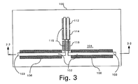
- FIG. 3 is a top view of an alternative embodiment of the antenna element in FIG. 1 and associated feed line circuitry.
- FIG. 4 is a flow chart that is useful for illustrating a process for manufacturing an antenna of reduced physical size and high radiation efficiency.
- FIG. 5 is a top view of an alternative embodiment of the invention in which a capacitor has been added between the antenna elements to improve the impedance bandwidth.
- FIG. 6 is a cross-sectional view of the alternative embodiment of FIG. 5 taken along line 6 — 6 .
- FIG. 7 is a top view of a further alternative embodiment of the invention in which a series of reactive elements have been interposed along the length of a loop radiating element.
- FIG. 8 is a cross-sectional view of the alternative embodiment of FIG. 7 taken along line 8 — 8 .
- FIG. 9 is a top view of another alternative embodiment of the invention in which a sleeve element has been added.
- FIG. 10 is a cross-section view of the alternative embodiment of FIG. 9 taken along lines 10 — 10 .
- Low dielectric constant board materials are ordinarily selected for RF designs.
- polytetrafluoroethylene (PTFE) based composites such as RT/duroid® 6002 (dielectric constant of 2.94; loss tangent of 0.009) and RT/duroid® 5880 (dielectric constant of 2.2; loss tangent of 0.0007) are both available from Rogers Microwave Products, Advanced Circuit Materials Division, 100 S. Roosevelt Ave, Chandler, Ariz. 85226. Both of these materials are common board material choices.
- the above board materials provide dielectric layers having relatively low dielectric constants with accompanying low loss tangents.
- the present invention provides the circuit designer with an added level of flexibility by permitting use of a dielectric layer portion with selectively controlled permittivity and permeability properties optimized for efficiency. This added flexibility enables improved performance and antenna element density not otherwise possible.
- antenna 102 can be comprised of elements 103 .
- the elements 103 can be mounted on dielectric layer 100 as shown or, buried within the dielectric layer 100 .
- the antenna 102 is configured as a dipole, but it will be appreciated by those skilled in the art that the invention is not so limited.
- dielectric layer 100 includes first region 104 having a first relative permittivity, and a second region 106 having a second relative permittivity.
- the first relative permittivity can be different from the second relative permittivity, although the invention is not so limited.
- a ground plane 110 is preferably provided beneath the antenna 102 and can include openings for the passage of antenna feeds 108 .
- Dielectric material 100 has a thickness that defines an antenna height above ground. The thickness is approximately equal to the physical distance from antenna 102 to the underlying ground plane 110 .
- Antenna elements 103 and the second region 106 of the dielectric layer are configured so that at least a portion of the antenna elements are positioned on the second region 106 as shown. According to a preferred embodiment, a substantial portion of each antenna element is positioned on the second region 106 as shown.
- the second relative permittivity of the substrate in the second region 106 can be substantially larger than the first relative permittivity of the dielectric in the first region 104 .
- resonant length is roughly proportional to 1/ ⁇ square root over ( ⁇ r ) ⁇ where ⁇ r is the relative permittivity. Accordingly, selecting a higher value of relative permittivity can reduce the physical dimensions of the antenna.
- One problem with increasing the relative permittivity in second region 106 is that radiation efficiency of the antenna 102 can be reduced.
- Microstrip antennas printed on high dielectric constant and relatively thick substrates tend to exhibit poor radiation efficiency.
- dielectric substrate having higher values of relative permittivity With dielectric substrate having higher values of relative permittivity, a larger amount of the electromagnetic field is concentrated in the dielectric between the conductive antenna element and the ground plane. Poor radiation efficiency under such circumstances is often attributed in part to surface wave modes propagating along the air/substrate interface.
- the net antenna capacitance generally decreases because the area reduction more than offsets the increase in effective permittivity resulting from the use of a higher dielectric constant substrate portion.
- the present invention permits formation of dielectric substrates having one or more regions having significant magnetic permeability.
- Prior substrates generally included materials having relative magnetic permeabilities of approximately 1.
- the ability to selectively add significant magnetic permeability to portions of the dielectric substrate can be used to increase the inductance of nearby conductive traces, such as transmission lines and antenna elements. This flexibility can be used to improve RF system performance in a number of ways.
- dielectric substrate portions having significant relative magnetic permeability can be used to increase the inductance of the dipole elements to compensate for losses in radiation efficiency from use of a high dielectric substrate and the generally resulting higher capacitance. Accordingly, resonance can be obtained, or approached, at a desired frequency by use of a dielectric having a relative magnetic permeability larger than 1.
- the invention can be used to improve performance or obviate the need to add a discrete inductor to the system in an attempt to accomplish the same function.
- the permeability can be increased roughly in accordance with the square root of the permittivity. For example, if a substrate were selected with a permittivity of 9, a good starting point for an optimal permeability would be 3.
- the optimal values in any particular case will be dependent upon a variety of factors including the precise nature of the dielectric structure above and below the antenna elements, the dielectric and conductive structure surrounding the antenna elements, the height of the antenna above the ground plane, width of the dipole arm, and so on. Accordingly, a suitable combination of optimum values for permittivity and permeability can be determined experimentally and/or with computer modeling.
- the foregoing technique is not limited to use with dipole antennas such as those shown in FIGS. 1 and 2. Instead, the foregoing technique can be used to produce efficient antenna elements of reduced size in other types of substrate structures. For example, rather than residing exclusively on top of the substrate as shown in FIGS. 1 and 2, the antenna elements 103 can be partially or entirely embedded within the second region 106 of the dielectric layer.
- the relative permittivity and/or permeability of the dielectric in the second region 106 can be different from the relative permittivity and permeability of the first region 104 .
- at least a portion of the dielectric substrate 100 can be comprised of one or more additional regions on which additional circuitry can be provided.
- region 112 , 114 , 116 can support antenna feed circuitry 115 , which can include a balun, a feed line or an impedance transformer.
- Each region 112 , 114 , 116 can have a relative permittivity and permeability that is optimized for the physical and electrical characteristics required for each of the respective components.
- FIG. 7 a loop antenna element 700 having a feed point 506 and a matching balun 705 is shown mounted on a dielectric substrate 701 .
- a ground plane 703 can be provided beneath the substrate as illustrated.
- the dielectric substrate region 704 beneath the loop antenna element 700 can have a permittivity and permeability that is different from the surrounding substrate 701 .
- the increased permittivity in region 704 can reduce the size of the antenna element 700 for a given operating frequency.
- the permeability in region 704 can be increased in a manner similar to that described above with respect to the dipole antenna.
- FIG. 5 is a top view of an alternative embodiment of the invention in which the permittivity in region 500 can be selectively controlled.
- FIG. 6 is a cross-sectional view of the alternative embodiment of FIG. 5 taken along line 6 — 6 .
- Common reference numbers in FIGS. 1-2 and 5 - 6 are used to identify common elements in FIGS. 5 and 6.
- region 500 By selectively controlling the permittivity of the substrate in the region 500 as shown, it is possible to increase or decrease the inherent capacitance that exists between the ends 105 of dipole elements 103 . The result is an improved impedance bandwidth that cannot otherwise be achieved using conventional lumped element means.
- the limits of region 500 are shown in FIGS. 5 and 6 as extending only between the adjacent ends 105 of the antenna elements 103 . It will be appreciated by those skilled in the art that the invention is not so limited. Rather, the limits of region 500 can extend somewhat more or less relative to the ends of the dipole elements 105 without departing from the intended scope of the invention.
- the region 500 can include a portion of the region below the ends of antenna elements 105 . Alternatively, only a portion of the region between the ends 105 can be modified so as to have different permittivity characteristics.
- a similar technique for improving the impedance bandwidth can also be applied to loop antennas.
- loop antennas it is conventional to interpose capacitors along the conductive path defining the radiating element for the loop.
- the referenced capacitors would typically be connected between adjacent end portions 702 of antenna element 700 as shown in FIGS. 7 and 8.
- the capacitor values necessary to implement these techniques can become too small to permit use of lumped element components such as chip capacitors.
- the permittivity in regions 708 can be selectively controlled to adjust the inherent capacitive coupling that exists between end portions 702 .
- the permittivity of the substrate in regions 708 is increased, the inherent capacitance between ends 702 can be increased. In this way, the necessary capacitance can be provided to improve the impedance bandwidth by making use of, and selectively controlling, the inherent capacitance between end portions 702 .
- the region 708 can be somewhat smaller than, or can extend somewhat past, the limits defined by end portions 702 .
- FIGS. 9 and 10 Another alternative embodiment of the invention is illustrated in FIGS. 9 and 10 where dipole elements 902 are mounted on a substrate 900 .
- Dipole elements 902 can have a feed point 901 as is well known in the art.
- a ground plane 904 can be provided beneath the substrate as shown.
- improvements to the input impedance bandwidth of an antenna can be achieved by the use of capacitive and inductive coupling at the adjacent ends of dipole elements.
- this capacitive coupling is achieved using a modified dielectric region 906 with a higher permittivity as compared to surrounding substrate 900 . This higher permittivity can improve capacitive coupling between dipole elements 902 in much the same way as previously described relative to FIGS. 5 and 6.
- the invention can make use of a conventional sleeve element 908 to provide inductive coupling.
- the permeability of the modified dielectric region 906 can be selectively controlled.
- the permeability can be increased to have a value larger than 1.
- the permeability in region 906 can be controlled so as to vary along the length of the inductive element 908 .
- the coupling between the “sleeve” and the dipole arm can be improved and controlled by selectively adjusting the dielectric of the substrate between the sleeve and the dipole arm to improve the impedance bandwidth.
- inventive arrangements for integrating reactive capacitive and inductive components into a dielectric circuit board substrate are not limited for use with the antennas as shown. Rather, the invention can be used with a wide variety of other circuit board components requiring small amounts of carefully controlled inductance and capacitance.
- Dielectric substrate boards having metamaterial portions providing localized and selectable magnetic and dielectric properties can be prepared as shown in FIG. 4 .
- the dielectric board material can be prepared.
- at least a portion of the dielectric board material can be differentially modified using meta-materials, as described below, to reduce the physical size and achieve the best possible efficiency for the antenna elements and associated feed circuitry.
- a metal layer can be applied to define the conductive traces associated with the antenna elements and associated feed circuitry.
- Metamaterials refers to composite materials formed from the mixing or arrangement of two or more different materials at a very fine level, such as the Angstrom or nanometer level. Metamaterials allow tailoring of electromagnetic properties of the composite, which can be defined by effective electromagnetic parameters comprising effective electrical permittivity (or dielectric constant) and the effective magnetic permeability.
- Appropriate bulk dielectric substrate materials can be obtained from commercial materials manufacturers, such as DuPont and Ferro.
- the unprocessed material commonly called Green TapeTM
- Green TapeTM can be cut into sized portions from a bulk dielectric tape, such as into 6 inch by 6 inch portions.
- DuPont Microcircuit Materials provides Green Tape material systems, such as Low-Temperature Cofire Dielectric Tape. These substrate materials can be used to provide dielectric layers having relatively moderate dielectric constants with accompanying relatively low loss tangents for circuit operation at microwave frequencies once fired.
- features such as vias, voids, holes, or cavities can be punched through one or more layers of tape.
- Voids can be defined using mechanical means (e.g. punch) or directed energy means (e.g., laser drilling, photolithography), but voids can also be defined using any other suitable method.
- Some vias can reach through the entire thickness of the sized substrate, while some voids can reach only through varying portions of the substrate thickness.
- the vias can then be filled with metal or other dielectric or magnetic materials, or mixtures thereof, usually using stencils for precise placement.
- the individual layers of tape can be stacked together in a conventional process to produce a complete, multi-layer substrate.
- the choice of a metamaterial composition can provide effective dielectric constants over a relatively continuous range from less than 2 to about 2650.
- Materials with magnetic properties are also available.
- the relative effective magnetic permeability generally can range from about 4 to 116 for most practical RF applications.
- the relative effective magnetic permeability can be as low as about 2 or reach into the thousands.
- differentially modified refers to modifications, including dopants, to a dielectric substrate layer that result in at least one of the dielectric and magnetic properties being different at one portion of the substrate as compared to another portion.
- a differentially modified board substrate preferably includes one or more metamaterial containing regions.
- the modification can be selective modification where certain dielectric layer portions are modified to produce a first set of dielectric or magnetic properties, while other dielectric layer portions are modified differentially or left unmodified to provide dielectric and/or magnetic properties different from the first set of properties.
- Differential modification can be accomplished in a variety of different ways.
- a supplemental dielectric layer can be added to the dielectric layer.
- Techniques known in the art such as various spray technologies, spin-on technologies, various deposition technologies or sputtering can be used to apply the supplemental dielectric layer.
- the supplemental dielectric layer can be selectively added in localized regions, including inside voids or holes, or over the entire existing dielectric layer.
- a supplemental dielectric layer can be used for providing a substrate portion having an increased effective dielectric constant.
- the differential modifying step can further include locally adding additional material to the dielectric layer or supplemental dielectric layer.
- the addition of material can be used to further control the effective dielectric constant or magnetic properties of the dielectric layer to achieve a given design objective.
- the additional material can include a plurality of metallic and/or ceramic particles.
- Metal particles preferably include iron, tungsten, cobalt, vanadium, manganese, certain rare-earth metals, nickel or niobium particles.
- the particles are preferably nanometer size particles, generally having sub-micron physical dimensions, hereafter referred to as nanoparticles.
- the particles can preferably be organofunctionalized composite particles.
- organofunctionalized composite particles can include particles having metallic cores with electrically insulating coatings or electrically insulating cores with a metallic coating.
- Magnetic metamaterial particles that are generally suitable for controlling magnetic properties of dielectric layer for a variety of applications described herein include ferrite organoceramics (FexCyHz)-(Ca/Sr/Ba-Ceramic). These particles work well for applications in the frequency range of 8-40 GHz.
- niobium organoceramics (NbCyHz)-(Ca/Sr/Ba-Ceramic) are useful for the frequency range of 12-40 GHz.
- the materials designated for high frequency are also applicable to low frequency applications.
- coated particles are preferable for use with the present invention as they can aid in binding with a polymer (e.g. LCP) matrix or side chain moiety.
- the added particles can also be used to control the effective dielectric constant of the material. Using a fill ratio of composite particles from approximately 1 to 70%, it is possible to raise and possibly lower the dielectric constant of substrate dielectric layer and/or supplemental dielectric layer portions significantly. For example, adding organofunctionalized nanoparticles to a dielectric layer can be used to raise the dielectric constant of the modified dielectric layer portions.
- Particles can be applied by a variety of techniques including polyblending, mixing and filling with agitation.
- the dielectric constant may be raised from a nominal LCP value of 2 to as high as 10 by using a variety of particles with a fill ratio of up to about 70%.
- Metal oxides useful for this purpose can include aluminum oxide, calcium oxide, magnesium oxide, nickel oxide, zirconium oxide and niobium (II, IV and V) oxide.
- the selectable dielectric properties can be localized to areas as small as about 10 nanometers, or cover large area regions, including the entire board substrate surface.
- Conventional techniques such as lithography and etching along with deposition processing can be used for localized dielectric and magnetic property manipulation.
- Materials can be prepared mixed with other materials or including varying densities of voided regions (which generally introduce air) to produce effective dielectric constants in a substantially continuous range from 2 to about 2650, as well as other potentially desired substrate properties.
- materials exhibiting a low dielectric constant include silica with varying densities of voided regions.
- Alumina with varying densities of voided regions can provide a dielectric constant of about 4 to 9.
- Neither silica nor alumina have any significant magnetic permeability.
- magnetic particles can be added, such as up to 20 wt. %, to render these or any other material significantly magnetic.
- magnetic properties may be tailored with organofunctionality. The impact on dielectric constant from adding magnetic materials generally results in an increase in the dielectric constant.
- Medium dielectric constant materials have a dielectric constant generally in the range of 70 to 500+/ ⁇ 10%. As noted above these materials may be mixed with other materials or voids to provide desired effective dielectric constant values. These materials can include ferrite doped calcium titanate. Doping metals can include magnesium, strontium and niobium. These materials have a range of 45 to 600 in relative magnetic permeability.
- ferrite or niobium doped calcium or barium titanate zirconates can be used. These materials have a dielectric constant of about 2200 to 2650. Doping percentages for these materials are generally from about 1 to 10%. As noted with respect to other materials, these materials may be mixed with other materials or voids to provide desired effective dielectric constant values.
- Modification processing can include void creation followed by filling with materials such as carbon and fluorine based organo functional materials, such as polytetrafluoroethylene PTFE.
- processing can include solid freeform fabrication (SFF), photo, uv, x-ray, e-beam or ion-beam irradiation.
- SFF solid freeform fabrication
- Lithography can also be performed using photo, uv, x-ray, e-beam or ion-beam radiation.
- Different materials including metamaterials, can be applied to different areas, so that a plurality of areas of the substrate layers have different dielectric and/or magnetic properties.
- the backfill materials such as noted above, may be used in conjunction with one or more additional processing steps to attain desired, dielectric and/or magnetic properties, either locally or over a bulk substrate portion.
- a top layer conductor print is then generally applied to the modified substrate layer.
- Conductor traces can be provided using thin film techniques, thick film techniques, electroplating or any other suitable technique.
- the processes used to define the conductor pattern include, but are not limited to standard lithography and stencil.
- a base plate is then generally obtained for collating and aligning a plurality of modified board substrates.
- the plurality of layers of substrate can then be laminated (e.g. mechanically pressed) together using either isostatic pressure, which puts pressure on the material from all directions, or uniaxial pressure, which puts pressure on the material from only one direction.
- the laminate substrate is then is further processed as described above or placed into an oven to be fired to a temperature suitable for the processed substrate (approximately 850 C. to 900 C. for the materials cited above).
- the plurality of ceramic tape layers can be controlled to rise in temperature at a rate suitable for the substrate materials used.
- the process conditions used such as the rate of increase in temperature, final temperature, cool down profile, and any necessary holds, are selected mindful of the substrate material and any material deposited thereon.
- stacked substrate boards typically, are inspected for flaws using an optical microscope.
- the stacked ceramic substrates can then be optionally diced into cingulated pieces as small as required to meet circuit functional requirements. Following final inspection, the cingulated substrate pieces can then be mounted to a test fixture for evaluation of their various characteristics, such as to assure that the dielectric, magnetic and/or electrical characteristics are within specified limits.
- dielectric substrate materials can be provided with localized tunable dielectric and/or magnetic characteristics for improving the density and performance of circuits.
- the dielectric flexibility allows independent optimization of the feed line impedance and dipole antenna elements.
Abstract
The invention concerns a dipole antenna of reduced size and with improved impedance bandwidth. The antenna is preferably formed on a dielectric substrate having a plurality of regions, each having a characteristic relative permeability and permittivity. First and second dipole radiating element defining conductive paths can be selectively formed on first characteristic regions of the substrate having a first characteristic permeability and first permittivity. A reactive coupling element can be interposed between the dipole radiating elements for reactively coupling the first dipole radiating element to the second dipole radiating element.
Description
1. Statement of the Technical Field
The inventive arrangements relate generally to methods and apparatus for providing increased design flexibility for RF circuits, and more particularly for optimization of dielectric circuit board materials for improved performance.
2. Description of the Related Art
RF circuits, transmission lines and antenna elements are commonly manufactured on specially designed substrate boards. For the purposes of these types of circuits, it is important to maintain careful control over impedance characteristics. If the impedance of different parts of the circuit do not match, this can result in inefficient power transfer, unnecessary heating of components, and other problems. Electrical length of transmission lines and radiators in these circuits can also be a critical design factor.
Two critical factors affecting the performance of a substrate material are dielectric constant (sometimes called the relative permittivity or ∈r) and the loss tangent (sometimes referred to as the dissipation factor). The relative permittivity determines the speed of the signal in the substrate material, and therefore the electrical length of transmission lines and other components implemented on the substrate. The loss tangent characterizes the amount of loss that occurs for signals traversing the substrate material. Losses tend to increase with increases in frequency. Accordingly, low loss materials become even more important with increasing frequency, particularly when designing receiver front ends and low noise amplifier circuits.
Printed transmission lines, passive circuits and radiating elements used in RF circuits are typically formed in one of three ways. One configuration known as microstrip, places the signal line on a board surface and provides a second conductive layer, commonly referred to as a ground plane. A second type of configuration known as buried microstrip is similar except that the signal line is covered with a dielectric substrate material. In a third configuration known as stripline, the signal line is sandwiched between two electrically conductive (ground) planes. Ignoring losses, the characteristic impedance of a transmission line, such as stripline or microstrip, is equal to {square root over (Ll/Cl)} where Ll is the inductance per unit length and Cl is the capacitance per unit length. The values of Ll and Cl are generally determined by the physical geometry and spacing of the line structure as well as the permittivity of the dielectric material(s) used to separate the transmission line structures. Conventional substrate materials typically have a permeability of approximately 1.0.
In conventional RF design, a substrate material is selected that has a relative permittivity value suitable for the design. Once the substrate material is selected, the line characteristic impedance value is exclusively adjusted by controlling the line geometry and physical structure.
Radio frequency (RF) circuits are typically embodied in hybrid circuits in which a plurality of active and passive circuit components are mounted and connected together on a surface of an electrically insulating board substrate such as a ceramic substrate. The various components are generally interconnected by printed metallic conductors of copper, gold, or tantalum, for example that are transmission lines as stripline or microstrip or twin-line structures.
The dielectric constant of the chosen substrate material for a transmission line, passive RF device, or radiating element determines the physical wavelength of RF energy at a given frequency for that line structure. One problem encountered when designing microelectronic RF circuitry is the selection of a dielectric board substrate material that is optimized for all of the various passive components, radiating elements and transmission line circuits to be formed on the board. In particular, the geometry of certain circuit elements may be physically large or miniaturized due to the unique electrical or impedance characteristics required for such elements. For example, many circuit elements or tuned circuits may need to be an electrical ¼ wave. Similarly, the line widths required for exceptionally high or low characteristic impedance values can, in many instances, be too narrow or too wide for practical implementation for a given substrate. Since the physical size of the microstrip or stripline is inversely related to the relative permittivity of the dielectric material, the dimensions of a transmission line can be affected greatly by the choice of substrate board material.
Still, an optimal board substrate material design choice for some components may be inconsistent with the optimal board substrate material for other components, such as antenna elements. Moreover, some design objectives for a circuit component may be inconsistent with one another. For example, it may be desirable to reduce the size of an antenna element. This could be accomplished by selecting a board material with a relatively high permittivity. However, the use of a dielectric with a higher relative permittivity will generally have the undesired effect of reducing the radiation efficiency of the antenna.
An antenna design goal is frequently to effectively reduce the size of the antenna without too great a reduction in radiation efficiency. One method of reducing antena size is through capacitive loading, such as through use of a high dielectric constant substrate for the dipole array elements.
For example, if dipole arms are capacitively loaded by placing them on “high” dielectric constant board substrate portions, the dipole arms can be shortened relative to the arm lengths which would otherwise be needed using a lower dielectric constant substrate. This effect results because the electrical field in high dielectric substrate portion between the arm portion and the ground plane will be concentrated into a smaller dielectric substrate volume.
However, the radiation efficiency, being the frequency dependent ratio of the power radiated by the antenna to the total power supplied to the antenna will be reduced primarily due to the shorter dipole arm length. A shorter arm length reduces the radiation resistance, which is approximately equal to the square of the arm length for a “short” (less the ½ wavelength) dipole antenna as shown below:
where l is the electrical length of the antenna line and λ is the wavelength of interest.
A conductive trace comprising a single short dipole can be modeled as an open transmission line having series connected radiation resistance, an inductor, a capacitor and a resistive ground loss. The radiation efficiency of a dipole antenna system, assuming a single mode can be approximated by the following equation: 
Where
E is the efficiency
Rr is the radiation resistance
XL is the inductive reactance
XC is the capacitive reactance
XL is the ohmic feed point ground losses and skin effect
The radiation resistance is a fictitious resistance that accounts for energy radiated by the antenna. The inductive reactance represents the inductance of the conductive dipole lines, while the capacitor is the capacitance between the conductors. The other series connected components simply turn RF energy into heat, which reduces the radiation efficiency of the dipole.
From the foregoing, it can be seen that the constraints of a circuit board substrate having selected relative dielectric properties often results in design compromises that can negatively affect the electrical performance and/or physical characteristics of the overall circuit. An inherent problem with the conventional approach is that, at least with respect to the substrate, the only control variable for line impedance is the relative permittivity. This limitation highlights an important problem with conventional substrate materials, i.e. they fail to take advantage of the other factor that determines characteristic impedance, namely Ll, the inductance per unit length of the transmission line.
Yet another problem that is encountered in RF circuit design is the optimization of circuit components for operation on different RF frequency bands. Line impedances and lengths that are optimized for a first RF frequency band may provide inferior performance when used for other bands, either due to impedance variations and/or variations in electrical length. Such limitations can limit the effective operational frequency range for a given RF system.
Conventional circuit board substrates are generally formed by processes such as casting or spray coating which generally result in uniform substrate physical properties, including the dielectric constant. Accordingly, conventional dielectric substrate arrangements for RF circuits have proven to be a limitation in designing circuits that are optimal in regards to both electrical and physical size characteristics.
The invention concerns a dipole antenna of reduced size and with improved impedance bandwidth. The antenna is preferably formed on a dielectric substrate having a plurality of regions, each having a characteristic relative permeability and permittivity. First and second dipole radiating element defining conductive paths can be selectively formed on first characteristic regions of the substrate having a first characteristic permeability and first permittivity. A reactive coupling element can be interposed between the dipole radiating elements for reactively coupling the first dipole radiating element to the second dipole radiating element.
The reactive coupling element is coupled to a second characteristic region of the substrate having a second permittivity and second permeability for providing a desired reactance value for the reactive coupling element. The reactive element can be comprised of at least one of a capacitor and an inductor. If the reactive element is comprised of a capacitor, the capacitive coupling can be provided as between adjacent ends of the dipole elements. The capacitive coupling is at least partially determined by the second relative permittivity.
The first and second characteristic regions are different from a third characteristic region of the substrate with regard to at least one of permeability and permittivity. According to one aspect of the invention, at least one of a third permittivity and a third permeability of the third characteristic region are smaller in value, respectively, as compared to at least one of the first and second permittivity and permeability. According to a second aspect of the invention, the third permittivity and third permeability are larger in value, respectively, as compared to at least one of the first and second permittivity and permeability.
According to another aspect of the invention, a metal sleeve element can be disposed on the second characteristic region of the substrate for inductively coupling adjacent ends of the dipole radiating elements. According to a preferred embodiment, the ends define an RF feed point for the dipole radiating elements. The metal sleeve element can be comprised of an elongated metal strip disposed adjacent to at least a portion of the dipole radiating elements. In any case, the inductive coupling is at least partially determined by the second relative permeability.
According to another aspect of the invention, the first permeability and the second permeability can be controlled by the addition of meta-materials to the dielectric substrate. Alternatively, or in addition thereto, the first permittivity and the second permittivity can be controlled by the addition of meta-materials to the dielectric substrate.
The invention can also include other types of antennas formed on dielectric substrates. According to an alternative embodiment, the antenna can be comprised of at least one radiating element, such as a loop, defining a conductive path and selectively formed on first characteristic regions of the substrate having a first characteristic permeability and first permittivity. One or more reactive coupling elements can be interposed between portions of the conductive path that are separated by a gap. The reactive coupling element can be coupled to a second characteristic region of the substrate having a second permittivity and second permeability for providing a desired reactance value for the reactive coupling element. Further, the first and second characteristic regions can be different from a third characteristic region of the substrate with regard to at least one of permeability and permittivity.
FIG. 1 is a top view of an antenna element formed on a substrate for reducing the size and improving the radiation efficiency of the element.
FIG. 2 is a cross-sectional view of an antenna element of FIG. 1 taken along line 2—2.
FIG. 3 is a top view of an alternative embodiment of the antenna element in FIG. 1 and associated feed line circuitry.
FIG. 4 is a flow chart that is useful for illustrating a process for manufacturing an antenna of reduced physical size and high radiation efficiency.
FIG. 5 is a top view of an alternative embodiment of the invention in which a capacitor has been added between the antenna elements to improve the impedance bandwidth.
FIG. 6 is a cross-sectional view of the alternative embodiment of FIG. 5 taken along line 6—6.
FIG. 7 is a top view of a further alternative embodiment of the invention in which a series of reactive elements have been interposed along the length of a loop radiating element.
FIG. 8 is a cross-sectional view of the alternative embodiment of FIG. 7 taken along line 8—8.
FIG. 9 is a top view of another alternative embodiment of the invention in which a sleeve element has been added.
FIG. 10 is a cross-section view of the alternative embodiment of FIG. 9 taken along lines 10—10.
Low dielectric constant board materials are ordinarily selected for RF designs. For example, polytetrafluoroethylene (PTFE) based composites such as RT/duroid® 6002 (dielectric constant of 2.94; loss tangent of 0.009) and RT/duroid® 5880 (dielectric constant of 2.2; loss tangent of 0.0007) are both available from Rogers Microwave Products, Advanced Circuit Materials Division, 100 S. Roosevelt Ave, Chandler, Ariz. 85226. Both of these materials are common board material choices. The above board materials provide dielectric layers having relatively low dielectric constants with accompanying low loss tangents.
However, use of conventional board materials can compromise the miniaturization of circuit elements and may also compromise some performance aspects of circuits that can benefit from high dielectric constant layers. A typical tradeoff in a communications circuit is between the physical size of antenna elements versus efficiency. By comparison, the present invention provides the circuit designer with an added level of flexibility by permitting use of a dielectric layer portion with selectively controlled permittivity and permeability properties optimized for efficiency. This added flexibility enables improved performance and antenna element density not otherwise possible.
Referring to FIG. 1, antenna 102 can be comprised of elements 103. The elements 103 can be mounted on dielectric layer 100 as shown or, buried within the dielectric layer 100. In FIG. 1, the antenna 102 is configured as a dipole, but it will be appreciated by those skilled in the art that the invention is not so limited. According to a preferred embodiment, dielectric layer 100 includes first region 104 having a first relative permittivity, and a second region 106 having a second relative permittivity. The first relative permittivity can be different from the second relative permittivity, although the invention is not so limited. A ground plane 110 is preferably provided beneath the antenna 102 and can include openings for the passage of antenna feeds 108. Alternatively, the feed line for the antenna can be disposed directly on the surface of the substrate as shown in FIG. 3. Dielectric material 100 has a thickness that defines an antenna height above ground. The thickness is approximately equal to the physical distance from antenna 102 to the underlying ground plane 110.
In order to reduce the physical size of the elements 103, the second relative permittivity of the substrate in the second region 106 can be substantially larger than the first relative permittivity of the dielectric in the first region 104. In general, resonant length is roughly proportional to 1/{square root over (∈r)} where ∈ r is the relative permittivity. Accordingly, selecting a higher value of relative permittivity can reduce the physical dimensions of the antenna.
One problem with increasing the relative permittivity in second region 106 is that radiation efficiency of the antenna 102 can be reduced. Microstrip antennas printed on high dielectric constant and relatively thick substrates tend to exhibit poor radiation efficiency. With dielectric substrate having higher values of relative permittivity, a larger amount of the electromagnetic field is concentrated in the dielectric between the conductive antenna element and the ground plane. Poor radiation efficiency under such circumstances is often attributed in part to surface wave modes propagating along the air/substrate interface.
As the size of the antenna is reduced through use of a high dielectric substrate, the net antenna capacitance generally decreases because the area reduction more than offsets the increase in effective permittivity resulting from the use of a higher dielectric constant substrate portion.
The present invention permits formation of dielectric substrates having one or more regions having significant magnetic permeability. Prior substrates generally included materials having relative magnetic permeabilities of approximately 1. The ability to selectively add significant magnetic permeability to portions of the dielectric substrate can be used to increase the inductance of nearby conductive traces, such as transmission lines and antenna elements. This flexibility can be used to improve RF system performance in a number of ways.
For example, in the case of short dipole antennas, dielectric substrate portions having significant relative magnetic permeability can be used to increase the inductance of the dipole elements to compensate for losses in radiation efficiency from use of a high dielectric substrate and the generally resulting higher capacitance. Accordingly, resonance can be obtained, or approached, at a desired frequency by use of a dielectric having a relative magnetic permeability larger than 1. Thus, the invention can be used to improve performance or obviate the need to add a discrete inductor to the system in an attempt to accomplish the same function.
In general it has been found that as substrate permittivity increases from 1, it is desirable to also increase permeability in order for the antenna to more effectively transfer electromagnetic energy from the antenna structure into free space. In this regard, it may be noted that variation in the dielectric constant or permittivity mainly affects the electric field whereas control over the permeability improves the transfer of energy for the magnetic field.
For greater radiation efficiency, it has been found that the permeability can be increased roughly in accordance with the square root of the permittivity. For example, if a substrate were selected with a permittivity of 9, a good starting point for an optimal permeability would be 3. Of course, those skilled in the art will recognize that the optimal values in any particular case will be dependent upon a variety of factors including the precise nature of the dielectric structure above and below the antenna elements, the dielectric and conductive structure surrounding the antenna elements, the height of the antenna above the ground plane, width of the dipole arm, and so on. Accordingly, a suitable combination of optimum values for permittivity and permeability can be determined experimentally and/or with computer modeling.
Those skilled in the art will recognize that the foregoing technique is not limited to use with dipole antennas such as those shown in FIGS. 1 and 2. Instead, the foregoing technique can be used to produce efficient antenna elements of reduced size in other types of substrate structures. For example, rather than residing exclusively on top of the substrate as shown in FIGS. 1 and 2, the antenna elements 103 can be partially or entirely embedded within the second region 106 of the dielectric layer.
According to a preferred embodiment, the relative permittivity and/or permeability of the dielectric in the second region 106 can be different from the relative permittivity and permeability of the first region 104. Further, at least a portion of the dielectric substrate 100 can be comprised of one or more additional regions on which additional circuitry can be provided. For example, in FIG. 3, region 112, 114, 116 can support antenna feed circuitry 115, which can include a balun, a feed line or an impedance transformer. Each region 112, 114, 116 can have a relative permittivity and permeability that is optimized for the physical and electrical characteristics required for each of the respective components.
Likewise, these techniques can be used for any other type of substrate antennas, the dipole of FIG. 1 being merely one example. Another example is a loop antenna, as shown in FIGS. 7 and 8, in which the permittivity and permeability of the substrate beneath the radiating elements and/or feed circuitry is selectively controlled for reduced size with high radiation efficiency. In FIG. 7 a loop antenna element 700 having a feed point 506 and a matching balun 705 is shown mounted on a dielectric substrate 701. A ground plane 703 can be provided beneath the substrate as illustrated. According to a preferred embodiment, the dielectric substrate region 704 beneath the loop antenna element 700 can have a permittivity and permeability that is different from the surrounding substrate 701. The increased permittivity in region 704 can reduce the size of the antenna element 700 for a given operating frequency. In order to maintain satisfactory radiation efficiency however, the permeability in region 704 can be increased in a manner similar to that described above with respect to the dipole antenna.
Alternatively, or in addition to, the modifications to the dielectric substrate beneath the antenna elements, other features of antenna performance can be improved by advantageously controlling the characteristics of selected portions of the substrate. For example, in conventional dipole antenna systems, it is known that a chip capacitor can be connected between the adjacent ends of the two antenna elements. The addition of a capacitor bridging the antenna elements in this location is advantageous as it can improve the impedance bandwidth of the antenna. Those skilled in the art are generally familiar with the techniques for selection of a suitable value of capacitance for achieving performance improvements. However, as operating frequencies increase, the necessary value of the coupling capacitor that would need to be provided between the adjacent ends can become extremely small. The result is that the proper capacitance value cannot be achieved using conventional lumped circuit components, such as chip capacitors.
Referring to FIG. 1, a certain amount of capacitance will inherently exist between the adjacent ends 105. However, the spacing of the ends 105 and the relatively low permittivity of the substrate 100 will generally be such that this inherent capacitance will not be the value necessary for optimizing the impedance bandwidth necessary for a particular application. Accordingly, FIG. 5 is a top view of an alternative embodiment of the invention in which the permittivity in region 500 can be selectively controlled. FIG. 6 is a cross-sectional view of the alternative embodiment of FIG. 5 taken along line 6—6. Common reference numbers in FIGS. 1-2 and 5-6 are used to identify common elements in FIGS. 5 and 6.
By selectively controlling the permittivity of the substrate in the region 500 as shown, it is possible to increase or decrease the inherent capacitance that exists between the ends 105 of dipole elements 103. The result is an improved impedance bandwidth that cannot otherwise be achieved using conventional lumped element means. The limits of region 500 are shown in FIGS. 5 and 6 as extending only between the adjacent ends 105 of the antenna elements 103. It will be appreciated by those skilled in the art that the invention is not so limited. Rather, the limits of region 500 can extend somewhat more or less relative to the ends of the dipole elements 105 without departing from the intended scope of the invention. For example, the region 500 can include a portion of the region below the ends of antenna elements 105. Alternatively, only a portion of the region between the ends 105 can be modified so as to have different permittivity characteristics.
A similar technique for improving the impedance bandwidth can also be applied to loop antennas. In the case of loop antennas, it is conventional to interpose capacitors along the conductive path defining the radiating element for the loop. In a conventional loop antenna, the referenced capacitors would typically be connected between adjacent end portions 702 of antenna element 700 as shown in FIGS. 7 and 8. However, as the design frequency of the antenna increases, the capacitor values necessary to implement these techniques can become too small to permit use of lumped element components such as chip capacitors.
According to a preferred embodiment shown in FIGS. 7 and 8, the permittivity in regions 708 can be selectively controlled to adjust the inherent capacitive coupling that exists between end portions 702. For example, if the permittivity of the substrate in regions 708 is increased, the inherent capacitance between ends 702 can be increased. In this way, the necessary capacitance can be provided to improve the impedance bandwidth by making use of, and selectively controlling, the inherent capacitance between end portions 702. Those skilled in the art will appreciate that the region 708 can be somewhat smaller than, or can extend somewhat past, the limits defined by end portions 702.
Another alternative embodiment of the invention is illustrated in FIGS. 9 and 10 where dipole elements 902 are mounted on a substrate 900. Dipole elements 902 can have a feed point 901 as is well known in the art. A ground plane 904 can be provided beneath the substrate as shown. It is known in the art that improvements to the input impedance bandwidth of an antenna can be achieved by the use of capacitive and inductive coupling at the adjacent ends of dipole elements. In FIGS. 9 and 10, this capacitive coupling is achieved using a modified dielectric region 906 with a higher permittivity as compared to surrounding substrate 900. This higher permittivity can improve capacitive coupling between dipole elements 902 in much the same way as previously described relative to FIGS. 5 and 6.
Further, the invention can make use of a conventional sleeve element 908 to provide inductive coupling. According to a preferred embodiment, however, the permeability of the modified dielectric region 906 can be selectively controlled. For example, the permeability can be increased to have a value larger than 1. Alternatively, the permeability in region 906 can be controlled so as to vary along the length of the inductive element 908. In any case, the coupling between the “sleeve” and the dipole arm can be improved and controlled by selectively adjusting the dielectric of the substrate between the sleeve and the dipole arm to improve the impedance bandwidth. The incorporation of permeable materials beneath the sleeve would allow for the control of line widths that might not otherwise be achievable without the use of magnetic materials. This control over the permittivity and permeability can provide the designer with greater flexibility to provide improved broadband impedance matching.
The inventive arrangements for integrating reactive capacitive and inductive components into a dielectric circuit board substrate are not limited for use with the antennas as shown. Rather, the invention can be used with a wide variety of other circuit board components requiring small amounts of carefully controlled inductance and capacitance.
Dielectric substrate boards having metamaterial portions providing localized and selectable magnetic and dielectric properties can be prepared as shown in FIG. 4. In step 410, the dielectric board material can be prepared. In step 420, at least a portion of the dielectric board material can be differentially modified using meta-materials, as described below, to reduce the physical size and achieve the best possible efficiency for the antenna elements and associated feed circuitry. Finally, a metal layer can be applied to define the conductive traces associated with the antenna elements and associated feed circuitry.
As defined herein, the term “metamaterials” refers to composite materials formed from the mixing or arrangement of two or more different materials at a very fine level, such as the Angstrom or nanometer level. Metamaterials allow tailoring of electromagnetic properties of the composite, which can be defined by effective electromagnetic parameters comprising effective electrical permittivity (or dielectric constant) and the effective magnetic permeability.
The process for preparing and differentially modifying the dielectric board material as described in steps 410 and 420 shall now be described in some detail. It should be understood, however, that the methods described herein are merely examples and the invention is not intended to be so limited.
Appropriate bulk dielectric substrate materials can be obtained from commercial materials manufacturers, such as DuPont and Ferro. The unprocessed material, commonly called Green Tape™, can be cut into sized portions from a bulk dielectric tape, such as into 6 inch by 6 inch portions. For example, DuPont Microcircuit Materials provides Green Tape material systems, such as Low-Temperature Cofire Dielectric Tape. These substrate materials can be used to provide dielectric layers having relatively moderate dielectric constants with accompanying relatively low loss tangents for circuit operation at microwave frequencies once fired.
In the process of creating a microwave circuit using multiple sheets of dielectric substrate material, features such as vias, voids, holes, or cavities can be punched through one or more layers of tape. Voids can be defined using mechanical means (e.g. punch) or directed energy means (e.g., laser drilling, photolithography), but voids can also be defined using any other suitable method. Some vias can reach through the entire thickness of the sized substrate, while some voids can reach only through varying portions of the substrate thickness.
The vias can then be filled with metal or other dielectric or magnetic materials, or mixtures thereof, usually using stencils for precise placement. The individual layers of tape can be stacked together in a conventional process to produce a complete, multi-layer substrate.
The choice of a metamaterial composition can provide effective dielectric constants over a relatively continuous range from less than 2 to about 2650. Materials with magnetic properties are also available. For example, through choice of suitable materials the relative effective magnetic permeability generally can range from about 4 to 116 for most practical RF applications. However, the relative effective magnetic permeability can be as low as about 2 or reach into the thousands.
The term “differentially modified” as used herein refers to modifications, including dopants, to a dielectric substrate layer that result in at least one of the dielectric and magnetic properties being different at one portion of the substrate as compared to another portion. A differentially modified board substrate preferably includes one or more metamaterial containing regions.
For example, the modification can be selective modification where certain dielectric layer portions are modified to produce a first set of dielectric or magnetic properties, while other dielectric layer portions are modified differentially or left unmodified to provide dielectric and/or magnetic properties different from the first set of properties. Differential modification can be accomplished in a variety of different ways.
According to one embodiment, a supplemental dielectric layer can be added to the dielectric layer. Techniques known in the art such as various spray technologies, spin-on technologies, various deposition technologies or sputtering can be used to apply the supplemental dielectric layer. The supplemental dielectric layer can be selectively added in localized regions, including inside voids or holes, or over the entire existing dielectric layer. For example, a supplemental dielectric layer can be used for providing a substrate portion having an increased effective dielectric constant.
The differential modifying step can further include locally adding additional material to the dielectric layer or supplemental dielectric layer. The addition of material can be used to further control the effective dielectric constant or magnetic properties of the dielectric layer to achieve a given design objective.
The additional material can include a plurality of metallic and/or ceramic particles. Metal particles preferably include iron, tungsten, cobalt, vanadium, manganese, certain rare-earth metals, nickel or niobium particles. The particles are preferably nanometer size particles, generally having sub-micron physical dimensions, hereafter referred to as nanoparticles.
The particles, such as nanoparticles, can preferably be organofunctionalized composite particles. For example, organofunctionalized composite particles can include particles having metallic cores with electrically insulating coatings or electrically insulating cores with a metallic coating. Magnetic metamaterial particles that are generally suitable for controlling magnetic properties of dielectric layer for a variety of applications described herein include ferrite organoceramics (FexCyHz)-(Ca/Sr/Ba-Ceramic). These particles work well for applications in the frequency range of 8-40 GHz. Alternatively, or in addition thereto, niobium organoceramics (NbCyHz)-(Ca/Sr/Ba-Ceramic) are useful for the frequency range of 12-40 GHz. The materials designated for high frequency are also applicable to low frequency applications. These and other types of composite particles can be obtained commercially.
In general, coated particles are preferable for use with the present invention as they can aid in binding with a polymer (e.g. LCP) matrix or side chain moiety. In addition to controlling the magnetic properties of the dielectric, the added particles can also be used to control the effective dielectric constant of the material. Using a fill ratio of composite particles from approximately 1 to 70%, it is possible to raise and possibly lower the dielectric constant of substrate dielectric layer and/or supplemental dielectric layer portions significantly. For example, adding organofunctionalized nanoparticles to a dielectric layer can be used to raise the dielectric constant of the modified dielectric layer portions.
Particles can be applied by a variety of techniques including polyblending, mixing and filling with agitation. For example, if the dielectric layer includes a LCP, the dielectric constant may be raised from a nominal LCP value of 2 to as high as 10 by using a variety of particles with a fill ratio of up to about 70%.
Metal oxides useful for this purpose can include aluminum oxide, calcium oxide, magnesium oxide, nickel oxide, zirconium oxide and niobium (II, IV and V) oxide. Lithium niobate (LiNbO3), and zirconates, such as calcium zirconate and magnesium zirconate, also may be used.
The selectable dielectric properties can be localized to areas as small as about 10 nanometers, or cover large area regions, including the entire board substrate surface. Conventional techniques such as lithography and etching along with deposition processing can be used for localized dielectric and magnetic property manipulation.
Materials can be prepared mixed with other materials or including varying densities of voided regions (which generally introduce air) to produce effective dielectric constants in a substantially continuous range from 2 to about 2650, as well as other potentially desired substrate properties. For example, materials exhibiting a low dielectric constant (<2 to about 4) include silica with varying densities of voided regions. Alumina with varying densities of voided regions can provide a dielectric constant of about 4 to 9. Neither silica nor alumina have any significant magnetic permeability. However, magnetic particles can be added, such as up to 20 wt. %, to render these or any other material significantly magnetic. For example, magnetic properties may be tailored with organofunctionality. The impact on dielectric constant from adding magnetic materials generally results in an increase in the dielectric constant.
Medium dielectric constant materials have a dielectric constant generally in the range of 70 to 500+/−10%. As noted above these materials may be mixed with other materials or voids to provide desired effective dielectric constant values. These materials can include ferrite doped calcium titanate. Doping metals can include magnesium, strontium and niobium. These materials have a range of 45 to 600 in relative magnetic permeability.
For high dielectric constant applications, ferrite or niobium doped calcium or barium titanate zirconates can be used. These materials have a dielectric constant of about 2200 to 2650. Doping percentages for these materials are generally from about 1 to 10%. As noted with respect to other materials, these materials may be mixed with other materials or voids to provide desired effective dielectric constant values.
These materials can generally be modified through various molecular modification processing. Modification processing can include void creation followed by filling with materials such as carbon and fluorine based organo functional materials, such as polytetrafluoroethylene PTFE.
Alternatively or in addition to organofunctional integration, processing can include solid freeform fabrication (SFF), photo, uv, x-ray, e-beam or ion-beam irradiation. Lithography can also be performed using photo, uv, x-ray, e-beam or ion-beam radiation.
Different materials, including metamaterials, can be applied to different areas, so that a plurality of areas of the substrate layers have different dielectric and/or magnetic properties. The backfill materials, such as noted above, may be used in conjunction with one or more additional processing steps to attain desired, dielectric and/or magnetic properties, either locally or over a bulk substrate portion.
A top layer conductor print is then generally applied to the modified substrate layer. Conductor traces can be provided using thin film techniques, thick film techniques, electroplating or any other suitable technique. The processes used to define the conductor pattern include, but are not limited to standard lithography and stencil.
A base plate is then generally obtained for collating and aligning a plurality of modified board substrates.
The plurality of layers of substrate can then be laminated (e.g. mechanically pressed) together using either isostatic pressure, which puts pressure on the material from all directions, or uniaxial pressure, which puts pressure on the material from only one direction. The laminate substrate is then is further processed as described above or placed into an oven to be fired to a temperature suitable for the processed substrate (approximately 850 C. to 900 C. for the materials cited above).
The plurality of ceramic tape layers can be controlled to rise in temperature at a rate suitable for the substrate materials used. The process conditions used, such as the rate of increase in temperature, final temperature, cool down profile, and any necessary holds, are selected mindful of the substrate material and any material deposited thereon. Following firing, stacked substrate boards, typically, are inspected for flaws using an optical microscope.
The stacked ceramic substrates can then be optionally diced into cingulated pieces as small as required to meet circuit functional requirements. Following final inspection, the cingulated substrate pieces can then be mounted to a test fixture for evaluation of their various characteristics, such as to assure that the dielectric, magnetic and/or electrical characteristics are within specified limits.
Thus, dielectric substrate materials can be provided with localized tunable dielectric and/or magnetic characteristics for improving the density and performance of circuits. The dielectric flexibility allows independent optimization of the feed line impedance and dipole antenna elements.
While the preferred embodiments of the invention have been illustrated and described, it will be clear that the invention is not so limited. Numerous modifications, changes, variations, substitutions and equivalents will occur to those skilled in the art without departing from the spirit and scope of the present invention as described in the claims.
Claims (20)
1. A dipole antenna with improved impedance bandwidth, comprising:
a dielectric substrate having a plurality of regions, each region having a characteristic permeability and permittivity;
a first and second dipole radiating element defining conductive paths and selectively formed on first characteristic regions of said substrate having a first permeability and a first permittivity;
a reactive coupling element interposed between said dipole radiating elements for reactively coupling said first dipole radiating element to said second dipole radiating element said reactive coupling element coupled to a second characteristic region of said substrate having a second permittivity and a second permeability for providing a desired reactance value for said reactive coupling element; and
wherein said first and second characteristic regions are different from a third characteristic region of said substrate with regard to permeability.
2. The antenna according to claim 1 wherein a third permeability of said third characteristic region is smaller in value as compared to at least one of said first and second permeability.
3. The antenna according to claim 1 wherein a third permeability of said third characteristic regions is larger in value as compared to at least one of said first and second permeability.
4. The antenna according to claim 1 wherein said reactive element is comprised of at least one of a capacitor and an inductor.
5. The antenna according to claim 1 wherein said reactive element is comprised of capacitive coupling between adjacent ends of said dipole elements.
6. The antenna according to claim 5 wherein said capacitive coupling is at least partially determined by said second permittivity.
7. The antenna according to claim 1 further comprising a metal sleeve element disposed on said second characteristic region of said substrate for inductively coupling adjacent ends of said dipole radiating elements.
8. The antenna according to claim 7 wherein said metal sleeve element is comprised of an elongated metal strip disposed adjacent to at least a portion of said dipole radiating elements.
9. The antenna according to claim 7 wherein said inductive coupling is at least partially determined by said second permeability.
10. The antenna according to claim 7 wherein said ends define an RF feed point for said dipole radiating elements.
11. The antenna according to claim 1 wherein at least one of said first permeability and said second permeability are controlled by the addition of meta-materials to said dielectric substrate.
12. The antenna according to claim 1 wherein at least one of said first permittivity and said second permittivity are controlled by the addition of meta-materials to said dielectric substrate.
13. An antenna, comprising;
a dielectric substrate having a plurality of regions, each having a characteristic permeability and permittivity;
at least one radiating element defining a conductive path and selectively formed on first characteristic regions of said substrate having a first permeability and first permittivity;
at least one reactive coupling element interposed between portions of said conductive path separated by a gap, said reactive coupling element coupled to a second characteristic region of said substrate having a second permittivity and second permeability for providing a desired reactance value for said reactive coupling element; and
wherein said first and second characteristic regions are different from a third characteristic region of said substrate with regard to permeability.
14. The antenna according to claim 13 wherein a third permeability of said third characteristic region is smaller in value as compared to at least one of said first and second permeability.
15. The antenna according to claim 13 wherein a third permeability of said third characteristic regions is larger in value as compared to at least one of said first and second permeability.
16. The antenna according to claim 13 wherein said reactive element is comprised of at least one of a capacitor and an inductor.
17. The antenna according to claim 13 wherein said reactive element is comprised of capacitive coupling between adjacent ends of said conductive path separated by said gap.
18. The antenna according to claim 17 wherein said capacitive coupling is at least partially determined by said second permittivity.
19. The antenna according to claim 13 wherein at least one of said first permeability and said second permeability are controlled by the addition of meta-materials to said dielectric substrate.
20. The antenna according to claim 13 wherein at least one of said first permittivity and said second permittivity are controlled by the addition of meta-materials to said dielectric substrate.
Priority Applications (7)
| Application Number | Priority Date | Filing Date | Title |
|---|---|---|---|
| US10/184,332 US6753814B2 (en) | 2002-06-27 | 2002-06-27 | Dipole arrangements using dielectric substrates of meta-materials |
| CA002431185A CA2431185C (en) | 2002-06-27 | 2003-06-05 | Dipole arrangements using dielectric substrates of meta-materials |
| AU2003204642A AU2003204642B2 (en) | 2002-06-27 | 2003-06-11 | Dipole arrangements using dielectric substrates of meta-materials |
| AT03012277T ATE352886T1 (en) | 2002-06-27 | 2003-06-11 | ANTENNA ON A DIELECTRIC SUBSTRATE WITH AREAS OF DIFFERENT DIELECTRICITY CONSTANT AND PERMEABILITY |
| EP03012277A EP1376759B1 (en) | 2002-06-27 | 2003-06-11 | Antenna on dielectric substrate comprising regions with different permittivity and permeability |
| DE60311360T DE60311360T2 (en) | 2002-06-27 | 2003-06-11 | Antenna on dielectric substrate with regions of different dielectric constant and permeability |
| JP2003179770A JP4142507B2 (en) | 2002-06-27 | 2003-06-24 | Dipole antenna using composite dielectric substrate |
Applications Claiming Priority (1)
| Application Number | Priority Date | Filing Date | Title |
|---|---|---|---|
| US10/184,332 US6753814B2 (en) | 2002-06-27 | 2002-06-27 | Dipole arrangements using dielectric substrates of meta-materials |
Publications (2)
| Publication Number | Publication Date |
|---|---|
| US20040001027A1 US20040001027A1 (en) | 2004-01-01 |
| US6753814B2 true US6753814B2 (en) | 2004-06-22 |
Family
ID=29717957
Family Applications (1)
| Application Number | Title | Priority Date | Filing Date |
|---|---|---|---|
| US10/184,332 Expired - Lifetime US6753814B2 (en) | 2002-06-27 | 2002-06-27 | Dipole arrangements using dielectric substrates of meta-materials |
Country Status (7)
| Country | Link |
|---|---|
| US (1) | US6753814B2 (en) |
| EP (1) | EP1376759B1 (en) |
| JP (1) | JP4142507B2 (en) |
| AT (1) | ATE352886T1 (en) |
| AU (1) | AU2003204642B2 (en) |
| CA (1) | CA2431185C (en) |
| DE (1) | DE60311360T2 (en) |
Cited By (67)
| Publication number | Priority date | Publication date | Assignee | Title |
|---|---|---|---|---|
| US20040150565A1 (en) * | 2003-01-31 | 2004-08-05 | Cristian Paun | Printed circuit board dipole antenna structure with impedance matching trace |
| US20050110697A1 (en) * | 2003-11-20 | 2005-05-26 | Chang-Jung Lee | Dipole antenna |
| WO2005076962A2 (en) * | 2004-02-05 | 2005-08-25 | Amphenol-T & M Antennas | Small footprint dual band dipole antennas for wireless networking |
| US20050225492A1 (en) * | 2004-03-05 | 2005-10-13 | Carsten Metz | Phased array metamaterial antenna system |
| US20050275594A1 (en) * | 2004-05-24 | 2005-12-15 | Amphenol-T&M Antennas | Multiple band antenna and antenna assembly |
| US20060038735A1 (en) * | 2004-08-18 | 2006-02-23 | Victor Shtrom | System and method for a minimized antenna apparatus with selectable elements |
| US20060038734A1 (en) * | 2004-08-18 | 2006-02-23 | Video54 Technologies, Inc. | System and method for an omnidirectional planar antenna apparatus with selectable elements |
| US20060040707A1 (en) * | 2004-08-18 | 2006-02-23 | Video54 Technologies, Inc. | System and method for transmission parameter control for an antenna apparatus with selectable elements |
| US20060098613A1 (en) * | 2004-11-05 | 2006-05-11 | Video54 Technologies, Inc. | Systems and methods for improved data throughput in communications networks |
| US20060109067A1 (en) * | 2004-11-22 | 2006-05-25 | Ruckus Wireless, Inc. | Circuit board having a pereipheral antenna apparatus with selectable antenna elements and selectable phase shifting |
| US20060109191A1 (en) * | 2004-11-22 | 2006-05-25 | Video54 Technologies, Inc. | Circuit board having a peripheral antenna apparatus with selectable antenna elements |
| US20060114167A1 (en) * | 2004-12-01 | 2006-06-01 | Z-Com, Inc. | Dipole antenna |
| US20060192720A1 (en) * | 2004-08-18 | 2006-08-31 | Ruckus Wireless, Inc. | Multiband omnidirectional planar antenna apparatus with selectable elements |
| US20070026807A1 (en) * | 2005-07-26 | 2007-02-01 | Ruckus Wireless, Inc. | Coverage enhancement using dynamic antennas |
| US20070115180A1 (en) * | 2004-08-18 | 2007-05-24 | William Kish | Transmission and reception parameter control |
| US20070249324A1 (en) * | 2006-04-24 | 2007-10-25 | Tyan-Shu Jou | Dynamic authentication in secured wireless networks |
| US20070252666A1 (en) * | 2006-04-28 | 2007-11-01 | Ruckus Wireless, Inc. | PIN diode network for multiband RF coupling |
| US20070287450A1 (en) * | 2006-04-24 | 2007-12-13 | Bo-Chieh Yang | Provisioned configuration for automatic wireless connection |
| US20070293178A1 (en) * | 2006-05-23 | 2007-12-20 | Darin Milton | Antenna Control |
| US7358912B1 (en) | 2005-06-24 | 2008-04-15 | Ruckus Wireless, Inc. | Coverage antenna apparatus with selectable horizontal and vertical polarization elements |
| US20080129640A1 (en) * | 2004-08-18 | 2008-06-05 | Ruckus Wireless, Inc. | Antennas with polarization diversity |
| US20080153416A1 (en) * | 2006-09-11 | 2008-06-26 | Takanori Washiro | Communication System and Communication Apparatus |
| US20080204349A1 (en) * | 2005-06-24 | 2008-08-28 | Victor Shtrom | Horizontal multiple-input multiple-output wireless antennas |
| US20080238800A1 (en) * | 2005-09-19 | 2008-10-02 | Brian Collins | Balanced Antenna Devices |
| US20100053010A1 (en) * | 2004-08-18 | 2010-03-04 | Victor Shtrom | Antennas with Polarization Diversity |
| US7696946B2 (en) | 2004-08-18 | 2010-04-13 | Ruckus Wireless, Inc. | Reducing stray capacitance in antenna element switching |
| US7965252B2 (en) | 2004-08-18 | 2011-06-21 | Ruckus Wireless, Inc. | Dual polarization antenna array with increased wireless coverage |
| US8009644B2 (en) | 2005-12-01 | 2011-08-30 | Ruckus Wireless, Inc. | On-demand services by wireless base station virtualization |
| US8031129B2 (en) | 2004-08-18 | 2011-10-04 | Ruckus Wireless, Inc. | Dual band dual polarization antenna array |
| US8217843B2 (en) | 2009-03-13 | 2012-07-10 | Ruckus Wireless, Inc. | Adjustment of radiation patterns utilizing a position sensor |
| US20120228563A1 (en) * | 2008-08-28 | 2012-09-13 | Alliant Techsystems Inc. | Composites for antennas and other applications |
| US8355343B2 (en) | 2008-01-11 | 2013-01-15 | Ruckus Wireless, Inc. | Determining associations in a mesh network |
| US8547899B2 (en) | 2007-07-28 | 2013-10-01 | Ruckus Wireless, Inc. | Wireless network throughput enhancement through channel aware scheduling |
| US8619662B2 (en) | 2004-11-05 | 2013-12-31 | Ruckus Wireless, Inc. | Unicast to multicast conversion |
| US8638708B2 (en) | 2004-11-05 | 2014-01-28 | Ruckus Wireless, Inc. | MAC based mapping in IP based communications |
| US8670725B2 (en) | 2006-08-18 | 2014-03-11 | Ruckus Wireless, Inc. | Closed-loop automatic channel selection |
| US8686905B2 (en) | 2007-01-08 | 2014-04-01 | Ruckus Wireless, Inc. | Pattern shaping of RF emission patterns |
| US8698675B2 (en) | 2009-05-12 | 2014-04-15 | Ruckus Wireless, Inc. | Mountable antenna elements for dual band antenna |
| US8756668B2 (en) | 2012-02-09 | 2014-06-17 | Ruckus Wireless, Inc. | Dynamic PSK for hotspots |
| US8824357B2 (en) | 2004-11-05 | 2014-09-02 | Ruckus Wireless, Inc. | Throughput enhancement by acknowledgment suppression |
| US9092610B2 (en) | 2012-04-04 | 2015-07-28 | Ruckus Wireless, Inc. | Key assignment for a brand |
| US9223908B2 (en) | 2011-12-28 | 2015-12-29 | Fujitsu Limited | Antenna designing method and apparatus |
| US9407012B2 (en) | 2010-09-21 | 2016-08-02 | Ruckus Wireless, Inc. | Antenna with dual polarization and mountable antenna elements |
| US9570799B2 (en) | 2012-09-07 | 2017-02-14 | Ruckus Wireless, Inc. | Multiband monopole antenna apparatus with ground plane aperture |
| US9634403B2 (en) | 2012-02-14 | 2017-04-25 | Ruckus Wireless, Inc. | Radio frequency emission pattern shaping |
| US9769655B2 (en) | 2006-04-24 | 2017-09-19 | Ruckus Wireless, Inc. | Sharing security keys with headless devices |
| US9792188B2 (en) | 2011-05-01 | 2017-10-17 | Ruckus Wireless, Inc. | Remote cable access point reset |
| US9847581B2 (en) | 2009-06-17 | 2017-12-19 | L. Pierre de Rochemont | Frequency-selective dipole antennas |
| US9979626B2 (en) | 2009-11-16 | 2018-05-22 | Ruckus Wireless, Inc. | Establishing a mesh network with wired and wireless links |
| US20180159239A1 (en) * | 2016-12-07 | 2018-06-07 | Wafer Llc | Low loss electrical transmission mechanism and antenna using same |
| US9999087B2 (en) | 2009-11-16 | 2018-06-12 | Ruckus Wireless, Inc. | Determining role assignment in a hybrid mesh network |
| US10186750B2 (en) | 2012-02-14 | 2019-01-22 | Arris Enterprises Llc | Radio frequency antenna array with spacing element |
| RU2681370C2 (en) * | 2014-01-15 | 2019-03-06 | Ханивелл Интернешнл Инк. | Anti-lightning-combined-stripline-circuit system |
| US10230161B2 (en) | 2013-03-15 | 2019-03-12 | Arris Enterprises Llc | Low-band reflector for dual band directional antenna |
| US10317558B2 (en) | 2017-03-14 | 2019-06-11 | Saudi Arabian Oil Company | EMU impulse antenna |
| US10330815B2 (en) | 2017-03-14 | 2019-06-25 | Saudi Arabian Oil Company | EMU impulse antenna for low frequency radio waves using giant dielectric and ferrite materials |
| US10338264B1 (en) | 2017-03-14 | 2019-07-02 | Saudi Arabian Oil Company | EMU impulse antenna with controlled directionality and improved impedance matching |
| US10365393B2 (en) | 2017-11-07 | 2019-07-30 | Saudi Arabian Oil Company | Giant dielectric nanoparticles as high contrast agents for electromagnetic (EM) fluids imaging in an oil reservoir |
| US10411324B2 (en) * | 2017-08-03 | 2019-09-10 | Quanta Computer Inc. | Antenna structure of a communications device |
| US10673130B2 (en) | 2004-10-01 | 2020-06-02 | L. Pierre de Rochemont | Ceramic antenna module and methods of manufacture thereof |
| USD940149S1 (en) | 2017-06-08 | 2022-01-04 | Insulet Corporation | Display screen with a graphical user interface |
| IL255523B (en) * | 2017-11-08 | 2022-09-01 | Mti Wireless Edge Ltd | Dual band antenna |
| USD977502S1 (en) | 2020-06-09 | 2023-02-07 | Insulet Corporation | Display screen with graphical user interface |
| US11857763B2 (en) | 2016-01-14 | 2024-01-02 | Insulet Corporation | Adjusting insulin delivery rates |
| US11865299B2 (en) | 2008-08-20 | 2024-01-09 | Insulet Corporation | Infusion pump systems and methods |
| US11929158B2 (en) | 2016-01-13 | 2024-03-12 | Insulet Corporation | User interface for diabetes management system |
| USD1020794S1 (en) | 2018-04-02 | 2024-04-02 | Bigfoot Biomedical, Inc. | Medication delivery device with icons |
Families Citing this family (119)
| Publication number | Priority date | Publication date | Assignee | Title |
|---|---|---|---|---|
| US8749054B2 (en) | 2010-06-24 | 2014-06-10 | L. Pierre de Rochemont | Semiconductor carrier with vertical power FET module |
| JP2006222873A (en) * | 2005-02-14 | 2006-08-24 | Tohoku Univ | Antenna, communication apparatus and method for manufacturing antenna |
| US8350657B2 (en) | 2005-06-30 | 2013-01-08 | Derochemont L Pierre | Power management module and method of manufacture |
| JP4945561B2 (en) | 2005-06-30 | 2012-06-06 | デ,ロシェモント,エル.,ピエール | Electrical component and method of manufacturing the same |
| US7519328B2 (en) | 2006-01-19 | 2009-04-14 | Murata Manufacturing Co., Ltd. | Wireless IC device and component for wireless IC device |
| US8354294B2 (en) | 2006-01-24 | 2013-01-15 | De Rochemont L Pierre | Liquid chemical deposition apparatus and process and products therefrom |
| DE112007000799B4 (en) * | 2006-04-10 | 2013-10-10 | Murata Mfg. Co., Ltd. | Wireless IC device |
| CN101346852B (en) | 2006-04-14 | 2012-12-26 | 株式会社村田制作所 | Wireless IC device |
| JP4135770B2 (en) * | 2006-04-14 | 2008-08-20 | 株式会社村田製作所 | antenna |
| EP2012388B1 (en) * | 2006-04-26 | 2011-12-28 | Murata Manufacturing Co. Ltd. | Article provided with feed circuit board |
| US9064198B2 (en) | 2006-04-26 | 2015-06-23 | Murata Manufacturing Co., Ltd. | Electromagnetic-coupling-module-attached article |
| JP4325744B2 (en) | 2006-05-26 | 2009-09-02 | 株式会社村田製作所 | Data combiner |
| CN101454989A (en) * | 2006-05-30 | 2009-06-10 | 株式会社村田制作所 | Information terminal |
| EP2023275B1 (en) | 2006-06-01 | 2011-04-27 | Murata Manufacturing Co. Ltd. | Radio frequency ic device and composite component for radio frequency ic device |
| WO2007145053A1 (en) * | 2006-06-12 | 2007-12-21 | Murata Manufacturing Co., Ltd. | Electromagnetically coupled module, wireless ic device inspecting system, electromagnetically coupled module using the wireless ic device inspecting system, and wireless ic device manufacturing method |
| JP4281850B2 (en) | 2006-06-30 | 2009-06-17 | 株式会社村田製作所 | optical disk |
| JP4957724B2 (en) * | 2006-07-11 | 2012-06-20 | 株式会社村田製作所 | Antenna and wireless IC device |
| WO2008023636A1 (en) | 2006-08-24 | 2008-02-28 | Murata Manufacturing Co., Ltd. | Wireless ic device inspecting system and wireless ic device manufacturing method using the same |
| JP4775442B2 (en) | 2006-09-26 | 2011-09-21 | 株式会社村田製作所 | Article with electromagnetic coupling module |
| WO2008050689A1 (en) * | 2006-10-27 | 2008-05-02 | Murata Manufacturing Co., Ltd. | Article with electromagnetically coupled module |
| WO2008090943A1 (en) | 2007-01-26 | 2008-07-31 | Murata Manufacturing Co., Ltd. | Container with electromagnetically coupling module |
| WO2008096576A1 (en) | 2007-02-06 | 2008-08-14 | Murata Manufacturing Co., Ltd. | Packing material provided with electromagnetically coupled module |
| JPWO2008096574A1 (en) * | 2007-02-06 | 2010-05-20 | 株式会社村田製作所 | Packaging material with electromagnetic coupling module |
| WO2008126458A1 (en) | 2007-04-06 | 2008-10-23 | Murata Manufacturing Co., Ltd. | Radio ic device |
| US8009101B2 (en) | 2007-04-06 | 2011-08-30 | Murata Manufacturing Co., Ltd. | Wireless IC device |
| JP4697332B2 (en) * | 2007-04-09 | 2011-06-08 | 株式会社村田製作所 | Wireless IC device |
| US8235299B2 (en) | 2007-07-04 | 2012-08-07 | Murata Manufacturing Co., Ltd. | Wireless IC device and component for wireless IC device |
| US7762472B2 (en) | 2007-07-04 | 2010-07-27 | Murata Manufacturing Co., Ltd | Wireless IC device |
| WO2008136226A1 (en) * | 2007-04-26 | 2008-11-13 | Murata Manufacturing Co., Ltd. | Wireless ic device |
| WO2008136220A1 (en) | 2007-04-27 | 2008-11-13 | Murata Manufacturing Co., Ltd. | Wireless ic device |
| KR101038132B1 (en) | 2007-04-27 | 2011-05-31 | 가부시키가이샤 무라타 세이사쿠쇼 | Wireless ic device |
| CN101675557B (en) | 2007-05-02 | 2013-03-13 | 株式会社村田制作所 | Antenna structure and wireless communication apparatus comprising the same |
| CN101568934A (en) | 2007-05-10 | 2009-10-28 | 株式会社村田制作所 | Wireless IC device |
| EP2148449B1 (en) | 2007-05-11 | 2012-12-12 | Murata Manufacturing Co., Ltd. | Wireless ic device |
| JP4396785B2 (en) * | 2007-06-27 | 2010-01-13 | 株式会社村田製作所 | Wireless IC device |
| CN101542831B (en) | 2007-07-09 | 2014-06-25 | 株式会社村田制作所 | Wireless ic device |
| CN104540317B (en) * | 2007-07-17 | 2018-11-02 | 株式会社村田制作所 | printed wiring substrate |
| US20090021352A1 (en) * | 2007-07-18 | 2009-01-22 | Murata Manufacturing Co., Ltd. | Radio frequency ic device and electronic apparatus |
| JP5104865B2 (en) * | 2007-07-18 | 2012-12-19 | 株式会社村田製作所 | Wireless IC device |
| WO2009011375A1 (en) | 2007-07-18 | 2009-01-22 | Murata Manufacturing Co., Ltd. | Wireless ic device and method for manufacturing the same |
| EP2086052B1 (en) * | 2007-07-18 | 2012-05-02 | Murata Manufacturing Co. Ltd. | Wireless ic device |
| US7830311B2 (en) | 2007-07-18 | 2010-11-09 | Murata Manufacturing Co., Ltd. | Wireless IC device and electronic device |
| US7932869B2 (en) * | 2007-08-17 | 2011-04-26 | Ethertronics, Inc. | Antenna with volume of material |
| WO2009081719A1 (en) | 2007-12-20 | 2009-07-02 | Murata Manufacturing Co., Ltd. | Radio ic device |
| CN101601169B (en) * | 2007-12-26 | 2013-08-14 | 株式会社村田制作所 | Antenna apparatus and wireless ic device |
| JP5267463B2 (en) | 2008-03-03 | 2013-08-21 | 株式会社村田製作所 | Wireless IC device and wireless communication system |
| JP4518211B2 (en) * | 2008-03-03 | 2010-08-04 | 株式会社村田製作所 | Compound antenna |
| CN101960665B (en) * | 2008-03-26 | 2014-03-26 | 株式会社村田制作所 | Radio IC device |
| EP2264831B1 (en) * | 2008-04-14 | 2020-05-27 | Murata Manufacturing Co. Ltd. | Radio ic device, electronic device, and method for adjusting resonance frequency of radio ic device |
| EP2284949B1 (en) * | 2008-05-21 | 2016-08-03 | Murata Manufacturing Co. Ltd. | Wireless ic device |
| WO2009142068A1 (en) * | 2008-05-22 | 2009-11-26 | 株式会社村田製作所 | Wireless ic device and method for manufacturing the same |
| CN104077622B (en) * | 2008-05-26 | 2016-07-06 | 株式会社村田制作所 | The authenticating method of wireless IC device system and Wireless IC device |
| JP4535210B2 (en) * | 2008-05-28 | 2010-09-01 | 株式会社村田製作所 | Wireless IC device component and wireless IC device |
| JP4557186B2 (en) | 2008-06-25 | 2010-10-06 | 株式会社村田製作所 | Wireless IC device and manufacturing method thereof |
| WO2010001987A1 (en) * | 2008-07-04 | 2010-01-07 | 株式会社村田製作所 | Wireless ic device |
| WO2010021217A1 (en) * | 2008-08-19 | 2010-02-25 | 株式会社村田製作所 | Wireless ic device and method for manufacturing same |
| JPWO2010023752A1 (en) * | 2008-08-29 | 2012-01-26 | パイオニア株式会社 | Longitudinal antenna |
| JP5429182B2 (en) * | 2008-10-24 | 2014-02-26 | 株式会社村田製作所 | Wireless IC device |
| DE112009002399B4 (en) * | 2008-10-29 | 2022-08-18 | Murata Manufacturing Co., Ltd. | Radio IC device |
| DE112009002384B4 (en) * | 2008-11-17 | 2021-05-06 | Murata Manufacturing Co., Ltd. | Antenna and wireless IC component |
| CN103500873B (en) | 2009-01-09 | 2016-08-31 | 株式会社村田制作所 | Wireless ic device and wireless ic module |
| DE112009003613B4 (en) * | 2009-01-16 | 2020-12-17 | Murata Manufacturing Co., Ltd. | IC COMPONENT |
| EP2385580B1 (en) | 2009-01-30 | 2014-04-09 | Murata Manufacturing Co., Ltd. | Antenna and wireless ic device |
| KR101591393B1 (en) * | 2009-03-03 | 2016-02-03 | 타이코 일렉트로닉스 서비시스 게엠베하 | Balanced metamaterial antenna device |
| JP5510450B2 (en) | 2009-04-14 | 2014-06-04 | 株式会社村田製作所 | Wireless IC device |
| JP4687832B2 (en) | 2009-04-21 | 2011-05-25 | 株式会社村田製作所 | Antenna device |
| JP5447515B2 (en) | 2009-06-03 | 2014-03-19 | 株式会社村田製作所 | Wireless IC device and manufacturing method thereof |
| US8922347B1 (en) | 2009-06-17 | 2014-12-30 | L. Pierre de Rochemont | R.F. energy collection circuit for wireless devices |
| JP5516580B2 (en) | 2009-06-19 | 2014-06-11 | 株式会社村田製作所 | Wireless IC device and method for coupling power feeding circuit and radiation plate |
| CN102474009B (en) | 2009-07-03 | 2015-01-07 | 株式会社村田制作所 | Antenna and antenna module |
| JP5182431B2 (en) | 2009-09-28 | 2013-04-17 | 株式会社村田製作所 | Wireless IC device and environmental state detection method using the same |
| CN102577646B (en) | 2009-09-30 | 2015-03-04 | 株式会社村田制作所 | Circuit substrate and method of manufacture thereof |
| JP5304580B2 (en) | 2009-10-02 | 2013-10-02 | 株式会社村田製作所 | Wireless IC device |
| WO2011045970A1 (en) | 2009-10-16 | 2011-04-21 | 株式会社村田製作所 | Antenna and wireless ic device |
| CN102598413A (en) | 2009-10-27 | 2012-07-18 | 株式会社村田制作所 | Transmitting/receiving apparatus and wireless tag reader |
| JP5333601B2 (en) | 2009-11-04 | 2013-11-06 | 株式会社村田製作所 | Communication terminal and information processing system |
| WO2011055702A1 (en) | 2009-11-04 | 2011-05-12 | 株式会社村田製作所 | Wireless ic tag, reader/writer, and information processing system |
| JP5327334B2 (en) | 2009-11-04 | 2013-10-30 | 株式会社村田製作所 | Communication terminal and information processing system |
| CN102576929B (en) * | 2009-11-20 | 2015-01-28 | 株式会社村田制作所 | Antenna device and mobile communication terminal |
| WO2011077877A1 (en) | 2009-12-24 | 2011-06-30 | 株式会社村田製作所 | Antenna and handheld terminal |
| JP5652470B2 (en) | 2010-03-03 | 2015-01-14 | 株式会社村田製作所 | Wireless communication module and wireless communication device |
| CN102782937B (en) | 2010-03-03 | 2016-02-17 | 株式会社村田制作所 | Wireless communication devices and wireless communication terminal |
| JP5477459B2 (en) | 2010-03-12 | 2014-04-23 | 株式会社村田製作所 | Wireless communication device and metal article |
| JP5370581B2 (en) | 2010-03-24 | 2013-12-18 | 株式会社村田製作所 | RFID system |
| JP5630499B2 (en) | 2010-03-31 | 2014-11-26 | 株式会社村田製作所 | Antenna apparatus and wireless communication device |
| JP5170156B2 (en) | 2010-05-14 | 2013-03-27 | 株式会社村田製作所 | Wireless IC device |
| JP5299351B2 (en) | 2010-05-14 | 2013-09-25 | 株式会社村田製作所 | Wireless IC device |
| US8552708B2 (en) | 2010-06-02 | 2013-10-08 | L. Pierre de Rochemont | Monolithic DC/DC power management module with surface FET |
| FI20105656A0 (en) * | 2010-06-10 | 2010-06-10 | Valtion Teknillinen | Dielectric end load of an antenna |
| JP5376060B2 (en) | 2010-07-08 | 2013-12-25 | 株式会社村田製作所 | Antenna and RFID device |
| US9023493B2 (en) | 2010-07-13 | 2015-05-05 | L. Pierre de Rochemont | Chemically complex ablative max-phase material and method of manufacture |
| GB2495418B (en) | 2010-07-28 | 2017-05-24 | Murata Manufacturing Co | Antenna apparatus and communication terminal instrument |
| WO2012020748A1 (en) | 2010-08-10 | 2012-02-16 | 株式会社村田製作所 | Printed wire board and wireless communication system |
| US8779489B2 (en) | 2010-08-23 | 2014-07-15 | L. Pierre de Rochemont | Power FET with a resonant transistor gate |
| US20120218156A1 (en) * | 2010-09-01 | 2012-08-30 | Qualcomm Incorporated | On-frequency repeater |
| JP5234071B2 (en) | 2010-09-03 | 2013-07-10 | 株式会社村田製作所 | RFIC module |
| WO2012043432A1 (en) | 2010-09-30 | 2012-04-05 | 株式会社村田製作所 | Wireless ic device |
| CN105206919B (en) | 2010-10-12 | 2018-11-02 | 株式会社村田制作所 | Antenna assembly and terminal installation |
| CN102971909B (en) | 2010-10-21 | 2014-10-15 | 株式会社村田制作所 | Communication terminal device |
| EP2636069B1 (en) | 2010-11-03 | 2021-07-07 | L. Pierre De Rochemont | Semiconductor chip carriers with monolithically integrated quantum dot devices and method of manufacture thereof |
| CN105048058B (en) | 2011-01-05 | 2017-10-27 | 株式会社村田制作所 | Wireless communication devices |
| CN103299325B (en) | 2011-01-14 | 2016-03-02 | 株式会社村田制作所 | RFID chip package and RFID label tag |
| KR20120093035A (en) * | 2011-02-14 | 2012-08-22 | 주식회사 케이엠더블유 | Connecting device for strip-line |
| WO2012117843A1 (en) | 2011-02-28 | 2012-09-07 | 株式会社村田製作所 | Wireless communication device |
| JP5630566B2 (en) | 2011-03-08 | 2014-11-26 | 株式会社村田製作所 | Antenna device and communication terminal device |
| EP2618424A4 (en) | 2011-04-05 | 2014-05-07 | Murata Manufacturing Co | Wireless communication device |
| WO2012141070A1 (en) | 2011-04-13 | 2012-10-18 | 株式会社村田製作所 | Wireless ic device and wireless communication terminal |
| JP5569648B2 (en) | 2011-05-16 | 2014-08-13 | 株式会社村田製作所 | Wireless IC device |
| EP3041087B1 (en) | 2011-07-14 | 2022-09-07 | Murata Manufacturing Co., Ltd. | Wireless communication device |
| WO2013011856A1 (en) | 2011-07-15 | 2013-01-24 | 株式会社村田製作所 | Wireless communication device |
| CN204189963U (en) | 2011-07-19 | 2015-03-04 | 株式会社村田制作所 | Antenna assembly and communication terminal |
| WO2013035821A1 (en) | 2011-09-09 | 2013-03-14 | 株式会社村田製作所 | Antenna device and wireless device |
| CN103380432B (en) | 2011-12-01 | 2016-10-19 | 株式会社村田制作所 | Wireless IC device and manufacture method thereof |
| CN103430382B (en) | 2012-01-30 | 2015-07-15 | 株式会社村田制作所 | Wireless IC device |
| JP5464307B2 (en) | 2012-02-24 | 2014-04-09 | 株式会社村田製作所 | ANTENNA DEVICE AND WIRELESS COMMUNICATION DEVICE |
| JP5304975B1 (en) | 2012-04-13 | 2013-10-02 | 株式会社村田製作所 | RFID tag inspection method and inspection apparatus |
| US10049799B2 (en) * | 2012-05-10 | 2018-08-14 | Emw Co., Ltd. | Magnetic sheet, method for manufacturing magnetic sheet and antenna comprising the magnetic sheet |
| TWI648544B (en) * | 2018-05-10 | 2019-01-21 | 矽品精密工業股份有限公司 | Test structure for testing RF components |
| TWI704714B (en) * | 2019-07-16 | 2020-09-11 | 啓碁科技股份有限公司 | Antenna system |
Citations (22)
| Publication number | Priority date | Publication date | Assignee | Title |
|---|---|---|---|---|
| US3571722A (en) | 1967-09-08 | 1971-03-23 | Texas Instruments Inc | Strip line compensated balun and circuits formed therewith |
| US3678418A (en) | 1971-07-28 | 1972-07-18 | Rca Corp | Printed circuit balun |
| US4495505A (en) | 1983-05-10 | 1985-01-22 | The United States Of America As Represented By The Secretary Of The Air Force | Printed circuit balun with a dipole antenna |
| US4525720A (en) | 1982-10-15 | 1985-06-25 | The United States Of America As Represented By The Secretary Of The Navy | Integrated spiral antenna and printed circuit balun |
| US4800344A (en) | 1985-03-21 | 1989-01-24 | And Yet, Inc. | Balun |
| US4825220A (en) | 1986-11-26 | 1989-04-25 | General Electric Company | Microstrip fed printed dipole with an integral balun |
| US4882553A (en) | 1987-09-25 | 1989-11-21 | U.S. Philips Corp. | Microwave balun |
| US4916410A (en) | 1989-05-01 | 1990-04-10 | E-Systems, Inc. | Hybrid-balun for splitting/combining RF power |
| US4924236A (en) | 1987-11-03 | 1990-05-08 | Raytheon Company | Patch radiator element with microstrip balian circuit providing double-tuned impedance matching |
| US5039891A (en) | 1989-12-20 | 1991-08-13 | Hughes Aircraft Company | Planar broadband FET balun |
| US5148130A (en) | 1990-06-07 | 1992-09-15 | Dietrich James L | Wideband microstrip UHF balun |
| US5379006A (en) | 1993-06-11 | 1995-01-03 | The United States Of America As Represented By The Secretary Of The Army | Wideband (DC to GHz) balun |
| US5455545A (en) | 1993-12-07 | 1995-10-03 | Philips Electronics North America Corporation | Compact low-loss microwave balun |
| US5523728A (en) | 1994-08-17 | 1996-06-04 | The United States Of America As Represented By The Secretary Of The Army | Microstrip DC-to-GHZ field stacking balun |
| US5678219A (en) | 1991-03-29 | 1997-10-14 | E-Systems, Inc. | Integrated electronic warfare antenna receiver |
| US6052039A (en) | 1997-07-18 | 2000-04-18 | National Science Council | Lumped constant compensated high/low pass balanced-to-unbalanced transition |
| US6114940A (en) | 1997-06-17 | 2000-09-05 | Tdk Corporation | BALUN transformer core material, BALUN transformer core and BALUN transformer |
| US6133806A (en) | 1999-03-25 | 2000-10-17 | Industrial Technology Research Institute | Miniaturized balun transformer |
| US6137376A (en) | 1999-07-14 | 2000-10-24 | International Business Machines Corporation | Printed BALUN circuits |
| US6184845B1 (en) | 1996-11-27 | 2001-02-06 | Symmetricom, Inc. | Dielectric-loaded antenna |
| US6307509B1 (en) | 1999-05-17 | 2001-10-23 | Trimble Navigation Limited | Patch antenna with custom dielectric |
| US6501425B1 (en) * | 1999-09-09 | 2002-12-31 | Murrata Manufacturing Co., Ltd. | Surface-mounted type antenna and communication device including the same |
Family Cites Families (5)
| Publication number | Priority date | Publication date | Assignee | Title |
|---|---|---|---|---|
| DE3312638A1 (en) * | 1983-04-08 | 1984-10-18 | Rohde & Schwarz GmbH & Co KG, 8000 München | ANTENNA WITH ELECTRICALLY SHORTENED LINEAR SPOTLIGHT |
| US5453752A (en) * | 1991-05-03 | 1995-09-26 | Georgia Tech Research Corporation | Compact broadband microstrip antenna |
| CA2160286C (en) * | 1994-12-08 | 1999-01-26 | James Gifford Evans | Small antennas such as microstrip patch antennas |
| AU5769300A (en) * | 1999-06-29 | 2001-01-31 | Sun Microsystems, Inc. | Method and apparatus for adjusting electrical characteristics of signal traces in layered circuit boards |
| FR2803107B1 (en) * | 1999-12-22 | 2004-07-23 | Commissariat Energie Atomique | ANISOTROPIC COMPOSITE ANTENNA |
-
2002
- 2002-06-27 US US10/184,332 patent/US6753814B2/en not_active Expired - Lifetime
-
2003
- 2003-06-05 CA CA002431185A patent/CA2431185C/en not_active Expired - Fee Related
- 2003-06-11 DE DE60311360T patent/DE60311360T2/en not_active Expired - Lifetime
- 2003-06-11 AU AU2003204642A patent/AU2003204642B2/en not_active Ceased
- 2003-06-11 EP EP03012277A patent/EP1376759B1/en not_active Expired - Lifetime
- 2003-06-11 AT AT03012277T patent/ATE352886T1/en not_active IP Right Cessation
- 2003-06-24 JP JP2003179770A patent/JP4142507B2/en not_active Expired - Fee Related
Patent Citations (22)
| Publication number | Priority date | Publication date | Assignee | Title |
|---|---|---|---|---|
| US3571722A (en) | 1967-09-08 | 1971-03-23 | Texas Instruments Inc | Strip line compensated balun and circuits formed therewith |
| US3678418A (en) | 1971-07-28 | 1972-07-18 | Rca Corp | Printed circuit balun |
| US4525720A (en) | 1982-10-15 | 1985-06-25 | The United States Of America As Represented By The Secretary Of The Navy | Integrated spiral antenna and printed circuit balun |
| US4495505A (en) | 1983-05-10 | 1985-01-22 | The United States Of America As Represented By The Secretary Of The Air Force | Printed circuit balun with a dipole antenna |
| US4800344A (en) | 1985-03-21 | 1989-01-24 | And Yet, Inc. | Balun |
| US4825220A (en) | 1986-11-26 | 1989-04-25 | General Electric Company | Microstrip fed printed dipole with an integral balun |
| US4882553A (en) | 1987-09-25 | 1989-11-21 | U.S. Philips Corp. | Microwave balun |
| US4924236A (en) | 1987-11-03 | 1990-05-08 | Raytheon Company | Patch radiator element with microstrip balian circuit providing double-tuned impedance matching |
| US4916410A (en) | 1989-05-01 | 1990-04-10 | E-Systems, Inc. | Hybrid-balun for splitting/combining RF power |
| US5039891A (en) | 1989-12-20 | 1991-08-13 | Hughes Aircraft Company | Planar broadband FET balun |
| US5148130A (en) | 1990-06-07 | 1992-09-15 | Dietrich James L | Wideband microstrip UHF balun |
| US5678219A (en) | 1991-03-29 | 1997-10-14 | E-Systems, Inc. | Integrated electronic warfare antenna receiver |
| US5379006A (en) | 1993-06-11 | 1995-01-03 | The United States Of America As Represented By The Secretary Of The Army | Wideband (DC to GHz) balun |
| US5455545A (en) | 1993-12-07 | 1995-10-03 | Philips Electronics North America Corporation | Compact low-loss microwave balun |
| US5523728A (en) | 1994-08-17 | 1996-06-04 | The United States Of America As Represented By The Secretary Of The Army | Microstrip DC-to-GHZ field stacking balun |
| US6184845B1 (en) | 1996-11-27 | 2001-02-06 | Symmetricom, Inc. | Dielectric-loaded antenna |
| US6114940A (en) | 1997-06-17 | 2000-09-05 | Tdk Corporation | BALUN transformer core material, BALUN transformer core and BALUN transformer |
| US6052039A (en) | 1997-07-18 | 2000-04-18 | National Science Council | Lumped constant compensated high/low pass balanced-to-unbalanced transition |
| US6133806A (en) | 1999-03-25 | 2000-10-17 | Industrial Technology Research Institute | Miniaturized balun transformer |
| US6307509B1 (en) | 1999-05-17 | 2001-10-23 | Trimble Navigation Limited | Patch antenna with custom dielectric |
| US6137376A (en) | 1999-07-14 | 2000-10-24 | International Business Machines Corporation | Printed BALUN circuits |
| US6501425B1 (en) * | 1999-09-09 | 2002-12-31 | Murrata Manufacturing Co., Ltd. | Surface-mounted type antenna and communication device including the same |
Non-Patent Citations (21)
| Title |
|---|
| U.S. patent application Ser. No. 10/184,277, Killen et al., filed Jun. 27, 2002. |
| U.S. patent application Ser. No. 10/185,144, Killen et al., filed Jun. 27, 2002. |
| U.S. patent application Ser. No. 10/185,162, Rumpf Jr. et al., filed Jun. 27, 2002. |
| U.S. patent application Ser. No. 10/185,187, Killen et al., filed Jun. 27, 2002. |
| U.S. patent application Ser. No. 10/185,251, Parsche et al., filed Jun. 27, 2002. |
| U.S. patent application Ser. No. 10/185,266, Killen et al., filed Jun. 27, 2002. |
| U.S. patent application Ser. No. 10/185,273, Killen et al., filed Jun. 27, 2002. |
| U.S. patent application Ser. No. 10/185,275, Killen et al., filed Jun. 27, 2002. |
| U.S. patent application Ser. No. 10/185,443, Killen et al., filed Jun. 27, 2002. |
| U.S. patent application Ser. No. 10/185,459, Killen et al., filed Jun. 27, 2002. |
| U.S. patent application Ser. No. 10/185,480, Killen et al., filed Jun. 27, 2002. |
| U.S. patent application Ser. No. 10/185,824, Killen et al., filed Jun. 27, 2002. |
| U.S. patent application Ser. No. 10/185,847, Killen et al., filed Jun. 27, 2002. |
| U.S. patent application Ser. No. 10/185,855, Killen et al., filed Jun. 27, 2002. |
| U.S. patent application Ser. No. 10/308,500, Killen et al., filed Dec. 3, 2002. |
| U.S. patent application Ser. No. 10/373,935, Killen et al., filed Feb. 25, 2003. |
| U.S. patent application Ser. No. 10/404,285, Killen et al., filed Mar. 31, 2003. |
| U.S. patent application Ser. No. 10/404,960, Killen et al., filed Mar. 31, 2003. |
| U.S. patent application Ser. No. 10/404,981, Killen et al., filed Mar. 31, 2003. |
| U.S. patent application Ser. No. 10/439,094, Delgado et al., filed May 15, 2003. |
| U.S. patent application Ser. No. 10/448,973, Delgado et al., filed May 30, 2003. |
Cited By (157)
| Publication number | Priority date | Publication date | Assignee | Title |
|---|---|---|---|---|
| US6943749B2 (en) * | 2003-01-31 | 2005-09-13 | M&Fc Holding, Llc | Printed circuit board dipole antenna structure with impedance matching trace |
| US20040150565A1 (en) * | 2003-01-31 | 2004-08-05 | Cristian Paun | Printed circuit board dipole antenna structure with impedance matching trace |
| US20050110697A1 (en) * | 2003-11-20 | 2005-05-26 | Chang-Jung Lee | Dipole antenna |
| US6956536B2 (en) * | 2003-11-20 | 2005-10-18 | Accton Technology Corporation | Dipole antenna |
| WO2005076962A2 (en) * | 2004-02-05 | 2005-08-25 | Amphenol-T & M Antennas | Small footprint dual band dipole antennas for wireless networking |
| US20050237255A1 (en) * | 2004-02-05 | 2005-10-27 | Amphenol-T&M Antennas | Small footprint dual band dipole antennas for wireless networking |
| WO2005076962A3 (en) * | 2004-02-05 | 2006-02-09 | Amphenol T & M Antennas | Small footprint dual band dipole antennas for wireless networking |
| US20050225492A1 (en) * | 2004-03-05 | 2005-10-13 | Carsten Metz | Phased array metamaterial antenna system |
| US6958729B1 (en) * | 2004-03-05 | 2005-10-25 | Lucent Technologies Inc. | Phased array metamaterial antenna system |
| US7161538B2 (en) | 2004-05-24 | 2007-01-09 | Amphenol-T&M Antennas | Multiple band antenna and antenna assembly |
| US20050275594A1 (en) * | 2004-05-24 | 2005-12-15 | Amphenol-T&M Antennas | Multiple band antenna and antenna assembly |
| US20070115180A1 (en) * | 2004-08-18 | 2007-05-24 | William Kish | Transmission and reception parameter control |
| US8583183B2 (en) | 2004-08-18 | 2013-11-12 | Ruckus Wireless, Inc. | Transmission and reception parameter control |
| US20100053010A1 (en) * | 2004-08-18 | 2010-03-04 | Victor Shtrom | Antennas with Polarization Diversity |
| US10187307B2 (en) | 2004-08-18 | 2019-01-22 | Arris Enterprises Llc | Transmission and reception parameter control |
| US10181655B2 (en) | 2004-08-18 | 2019-01-15 | Arris Enterprises Llc | Antenna with polarization diversity |
| US9837711B2 (en) | 2004-08-18 | 2017-12-05 | Ruckus Wireless, Inc. | Antenna with selectable elements for use in wireless communications |
| US20060192720A1 (en) * | 2004-08-18 | 2006-08-31 | Ruckus Wireless, Inc. | Multiband omnidirectional planar antenna apparatus with selectable elements |
| US9484638B2 (en) | 2004-08-18 | 2016-11-01 | Ruckus Wireless, Inc. | Transmission and reception parameter control |
| US20060038734A1 (en) * | 2004-08-18 | 2006-02-23 | Video54 Technologies, Inc. | System and method for an omnidirectional planar antenna apparatus with selectable elements |
| US9153876B2 (en) | 2004-08-18 | 2015-10-06 | Ruckus Wireless, Inc. | Transmission and reception parameter control |
| US9077071B2 (en) | 2004-08-18 | 2015-07-07 | Ruckus Wireless, Inc. | Antenna with polarization diversity |
| US7652632B2 (en) | 2004-08-18 | 2010-01-26 | Ruckus Wireless, Inc. | Multiband omnidirectional planar antenna apparatus with selectable elements |
| US9019165B2 (en) | 2004-08-18 | 2015-04-28 | Ruckus Wireless, Inc. | Antenna with selectable elements for use in wireless communications |
| US8860629B2 (en) | 2004-08-18 | 2014-10-14 | Ruckus Wireless, Inc. | Dual band dual polarization antenna array |
| US20060038735A1 (en) * | 2004-08-18 | 2006-02-23 | Victor Shtrom | System and method for a minimized antenna apparatus with selectable elements |
| US7292198B2 (en) | 2004-08-18 | 2007-11-06 | Ruckus Wireless, Inc. | System and method for an omnidirectional planar antenna apparatus with selectable elements |
| US8594734B2 (en) | 2004-08-18 | 2013-11-26 | Ruckus Wireless, Inc. | Transmission and reception parameter control |
| US20060040707A1 (en) * | 2004-08-18 | 2006-02-23 | Video54 Technologies, Inc. | System and method for transmission parameter control for an antenna apparatus with selectable elements |
| US8314749B2 (en) | 2004-08-18 | 2012-11-20 | Ruckus Wireless, Inc. | Dual band dual polarization antenna array |
| US7362280B2 (en) * | 2004-08-18 | 2008-04-22 | Ruckus Wireless, Inc. | System and method for a minimized antenna apparatus with selectable elements |
| US20080129640A1 (en) * | 2004-08-18 | 2008-06-05 | Ruckus Wireless, Inc. | Antennas with polarization diversity |
| US8031129B2 (en) | 2004-08-18 | 2011-10-04 | Ruckus Wireless, Inc. | Dual band dual polarization antenna array |
| US20080136725A1 (en) * | 2004-08-18 | 2008-06-12 | Victor Shtrom | Minimized Antenna Apparatus with Selectable Elements |
| US7965252B2 (en) | 2004-08-18 | 2011-06-21 | Ruckus Wireless, Inc. | Dual polarization antenna array with increased wireless coverage |
| US7933628B2 (en) | 2004-08-18 | 2011-04-26 | Ruckus Wireless, Inc. | Transmission and reception parameter control |
| US7899497B2 (en) | 2004-08-18 | 2011-03-01 | Ruckus Wireless, Inc. | System and method for transmission parameter control for an antenna apparatus with selectable elements |
| US20090022066A1 (en) * | 2004-08-18 | 2009-01-22 | Kish William S | Transmission parameter control for an antenna apparatus with selectable elements |
| US7498996B2 (en) | 2004-08-18 | 2009-03-03 | Ruckus Wireless, Inc. | Antennas with polarization diversity |
| US7880683B2 (en) | 2004-08-18 | 2011-02-01 | Ruckus Wireless, Inc. | Antennas with polarization diversity |
| US7877113B2 (en) | 2004-08-18 | 2011-01-25 | Ruckus Wireless, Inc. | Transmission parameter control for an antenna apparatus with selectable elements |
| US7511680B2 (en) | 2004-08-18 | 2009-03-31 | Ruckus Wireless, Inc. | Minimized antenna apparatus with selectable elements |
| US20100091749A1 (en) * | 2004-08-18 | 2010-04-15 | William Kish | Transmission and Reception Parameter Control |
| US7696946B2 (en) | 2004-08-18 | 2010-04-13 | Ruckus Wireless, Inc. | Reducing stray capacitance in antenna element switching |
| US10673130B2 (en) | 2004-10-01 | 2020-06-02 | L. Pierre de Rochemont | Ceramic antenna module and methods of manufacture thereof |
| US8634402B2 (en) | 2004-11-05 | 2014-01-21 | Ruckus Wireless, Inc. | Distributed access point for IP based communications |
| US8824357B2 (en) | 2004-11-05 | 2014-09-02 | Ruckus Wireless, Inc. | Throughput enhancement by acknowledgment suppression |
| US8619662B2 (en) | 2004-11-05 | 2013-12-31 | Ruckus Wireless, Inc. | Unicast to multicast conversion |
| US8638708B2 (en) | 2004-11-05 | 2014-01-28 | Ruckus Wireless, Inc. | MAC based mapping in IP based communications |
| US9071942B2 (en) | 2004-11-05 | 2015-06-30 | Ruckus Wireless, Inc. | MAC based mapping in IP based communications |
| US9794758B2 (en) | 2004-11-05 | 2017-10-17 | Ruckus Wireless, Inc. | Increasing reliable data throughput in a wireless network |
| US9066152B2 (en) | 2004-11-05 | 2015-06-23 | Ruckus Wireless, Inc. | Distributed access point for IP based communications |
| US7787436B2 (en) | 2004-11-05 | 2010-08-31 | Ruckus Wireless, Inc. | Communications throughput with multiple physical data rate transmission determinations |
| US9019886B2 (en) | 2004-11-05 | 2015-04-28 | Ruckus Wireless, Inc. | Unicast to multicast conversion |
| US7505447B2 (en) | 2004-11-05 | 2009-03-17 | Ruckus Wireless, Inc. | Systems and methods for improved data throughput in communications networks |
| US8125975B2 (en) | 2004-11-05 | 2012-02-28 | Ruckus Wireless, Inc. | Communications throughput with unicast packet transmission alternative |
| US20060098613A1 (en) * | 2004-11-05 | 2006-05-11 | Video54 Technologies, Inc. | Systems and methods for improved data throughput in communications networks |
| US8089949B2 (en) | 2004-11-05 | 2012-01-03 | Ruckus Wireless, Inc. | Distributed access point for IP based communications |
| US9661475B2 (en) | 2004-11-05 | 2017-05-23 | Ruckus Wireless, Inc. | Distributed access point for IP based communications |
| US20080137681A1 (en) * | 2004-11-05 | 2008-06-12 | Kish William S | Communications throughput with unicast packet transmission alternative |
| US9240868B2 (en) | 2004-11-05 | 2016-01-19 | Ruckus Wireless, Inc. | Increasing reliable data throughput in a wireless network |
| US20060109191A1 (en) * | 2004-11-22 | 2006-05-25 | Video54 Technologies, Inc. | Circuit board having a peripheral antenna apparatus with selectable antenna elements |
| US20060109067A1 (en) * | 2004-11-22 | 2006-05-25 | Ruckus Wireless, Inc. | Circuit board having a pereipheral antenna apparatus with selectable antenna elements and selectable phase shifting |
| US20070218953A1 (en) * | 2004-11-22 | 2007-09-20 | Victor Shtrom | Increased wireless coverage patterns |
| US7498999B2 (en) | 2004-11-22 | 2009-03-03 | Ruckus Wireless, Inc. | Circuit board having a peripheral antenna apparatus with selectable antenna elements and selectable phase shifting |
| US9379456B2 (en) | 2004-11-22 | 2016-06-28 | Ruckus Wireless, Inc. | Antenna array |
| US7525486B2 (en) | 2004-11-22 | 2009-04-28 | Ruckus Wireless, Inc. | Increased wireless coverage patterns |
| US7193562B2 (en) | 2004-11-22 | 2007-03-20 | Ruckus Wireless, Inc. | Circuit board having a peripheral antenna apparatus with selectable antenna elements |
| US20060114167A1 (en) * | 2004-12-01 | 2006-06-01 | Z-Com, Inc. | Dipole antenna |
| US7126540B2 (en) * | 2004-12-01 | 2006-10-24 | Z-Com Inc. | Dipole antenna |
| US9344161B2 (en) | 2004-12-09 | 2016-05-17 | Ruckus Wireless, Inc. | Coverage enhancement using dynamic antennas and virtual access points |
| US9093758B2 (en) | 2004-12-09 | 2015-07-28 | Ruckus Wireless, Inc. | Coverage antenna apparatus with selectable horizontal and vertical polarization elements |
| US9270029B2 (en) | 2005-01-21 | 2016-02-23 | Ruckus Wireless, Inc. | Pattern shaping of RF emission patterns |
| US10056693B2 (en) | 2005-01-21 | 2018-08-21 | Ruckus Wireless, Inc. | Pattern shaping of RF emission patterns |
| US7646343B2 (en) | 2005-06-24 | 2010-01-12 | Ruckus Wireless, Inc. | Multiple-input multiple-output wireless antennas |
| US7675474B2 (en) | 2005-06-24 | 2010-03-09 | Ruckus Wireless, Inc. | Horizontal multiple-input multiple-output wireless antennas |
| US8836606B2 (en) | 2005-06-24 | 2014-09-16 | Ruckus Wireless, Inc. | Coverage antenna apparatus with selectable horizontal and vertical polarization elements |
| US20080204349A1 (en) * | 2005-06-24 | 2008-08-28 | Victor Shtrom | Horizontal multiple-input multiple-output wireless antennas |
| US7358912B1 (en) | 2005-06-24 | 2008-04-15 | Ruckus Wireless, Inc. | Coverage antenna apparatus with selectable horizontal and vertical polarization elements |
| US9577346B2 (en) | 2005-06-24 | 2017-02-21 | Ruckus Wireless, Inc. | Vertical multiple-input multiple-output wireless antennas |
| US8704720B2 (en) | 2005-06-24 | 2014-04-22 | Ruckus Wireless, Inc. | Coverage antenna apparatus with selectable horizontal and vertical polarization elements |
| US8068068B2 (en) | 2005-06-24 | 2011-11-29 | Ruckus Wireless, Inc. | Coverage antenna apparatus with selectable horizontal and vertical polarization elements |
| US20070026807A1 (en) * | 2005-07-26 | 2007-02-01 | Ruckus Wireless, Inc. | Coverage enhancement using dynamic antennas |
| US8792414B2 (en) | 2005-07-26 | 2014-07-29 | Ruckus Wireless, Inc. | Coverage enhancement using dynamic antennas |
| US20080238800A1 (en) * | 2005-09-19 | 2008-10-02 | Brian Collins | Balanced Antenna Devices |
| US8009644B2 (en) | 2005-12-01 | 2011-08-30 | Ruckus Wireless, Inc. | On-demand services by wireless base station virtualization |
| US8923265B2 (en) | 2005-12-01 | 2014-12-30 | Ruckus Wireless, Inc. | On-demand services by wireless base station virtualization |
| US9313798B2 (en) | 2005-12-01 | 2016-04-12 | Ruckus Wireless, Inc. | On-demand services by wireless base station virtualization |
| US8605697B2 (en) | 2005-12-01 | 2013-12-10 | Ruckus Wireless, Inc. | On-demand services by wireless base station virtualization |
| US20090092255A1 (en) * | 2006-04-24 | 2009-04-09 | Ruckus Wireless, Inc. | Dynamic Authentication in Secured Wireless Networks |
| US9769655B2 (en) | 2006-04-24 | 2017-09-19 | Ruckus Wireless, Inc. | Sharing security keys with headless devices |
| US20070249324A1 (en) * | 2006-04-24 | 2007-10-25 | Tyan-Shu Jou | Dynamic authentication in secured wireless networks |
| US8607315B2 (en) | 2006-04-24 | 2013-12-10 | Ruckus Wireless, Inc. | Dynamic authentication in secured wireless networks |
| US7788703B2 (en) | 2006-04-24 | 2010-08-31 | Ruckus Wireless, Inc. | Dynamic authentication in secured wireless networks |
| US9131378B2 (en) | 2006-04-24 | 2015-09-08 | Ruckus Wireless, Inc. | Dynamic authentication in secured wireless networks |
| US8272036B2 (en) | 2006-04-24 | 2012-09-18 | Ruckus Wireless, Inc. | Dynamic authentication in secured wireless networks |
| US9071583B2 (en) | 2006-04-24 | 2015-06-30 | Ruckus Wireless, Inc. | Provisioned configuration for automatic wireless connection |
| US20070287450A1 (en) * | 2006-04-24 | 2007-12-13 | Bo-Chieh Yang | Provisioned configuration for automatic wireless connection |
| US7669232B2 (en) | 2006-04-24 | 2010-02-23 | Ruckus Wireless, Inc. | Dynamic authentication in secured wireless networks |
| US20070252666A1 (en) * | 2006-04-28 | 2007-11-01 | Ruckus Wireless, Inc. | PIN diode network for multiband RF coupling |
| US7639106B2 (en) | 2006-04-28 | 2009-12-29 | Ruckus Wireless, Inc. | PIN diode network for multiband RF coupling |
| US20070293178A1 (en) * | 2006-05-23 | 2007-12-20 | Darin Milton | Antenna Control |
| US9780813B2 (en) | 2006-08-18 | 2017-10-03 | Ruckus Wireless, Inc. | Closed-loop automatic channel selection |
| US8670725B2 (en) | 2006-08-18 | 2014-03-11 | Ruckus Wireless, Inc. | Closed-loop automatic channel selection |
| US20080153416A1 (en) * | 2006-09-11 | 2008-06-26 | Takanori Washiro | Communication System and Communication Apparatus |
| US20110110404A1 (en) * | 2006-09-11 | 2011-05-12 | Sony Corporation | Communication system and communication apparatus |
| US8238824B2 (en) | 2006-09-11 | 2012-08-07 | Sony Corporation | Communication system and communication apparatus |
| US7894770B2 (en) | 2006-09-11 | 2011-02-22 | Sony Corporation | Communication system and communication apparatus |
| US8686905B2 (en) | 2007-01-08 | 2014-04-01 | Ruckus Wireless, Inc. | Pattern shaping of RF emission patterns |
| US9271327B2 (en) | 2007-07-28 | 2016-02-23 | Ruckus Wireless, Inc. | Wireless network throughput enhancement through channel aware scheduling |
| US8547899B2 (en) | 2007-07-28 | 2013-10-01 | Ruckus Wireless, Inc. | Wireless network throughput enhancement through channel aware scheduling |
| US9674862B2 (en) | 2007-07-28 | 2017-06-06 | Ruckus Wireless, Inc. | Wireless network throughput enhancement through channel aware scheduling |
| US8780760B2 (en) | 2008-01-11 | 2014-07-15 | Ruckus Wireless, Inc. | Determining associations in a mesh network |
| US8355343B2 (en) | 2008-01-11 | 2013-01-15 | Ruckus Wireless, Inc. | Determining associations in a mesh network |
| US11865299B2 (en) | 2008-08-20 | 2024-01-09 | Insulet Corporation | Infusion pump systems and methods |
| US9263804B2 (en) | 2008-08-28 | 2016-02-16 | Orbital Atk, Inc. | Composites for antennas and other applications |
| US8723722B2 (en) * | 2008-08-28 | 2014-05-13 | Alliant Techsystems Inc. | Composites for antennas and other applications |
| US20120228563A1 (en) * | 2008-08-28 | 2012-09-13 | Alliant Techsystems Inc. | Composites for antennas and other applications |
| US8723741B2 (en) | 2009-03-13 | 2014-05-13 | Ruckus Wireless, Inc. | Adjustment of radiation patterns utilizing a position sensor |
| US8217843B2 (en) | 2009-03-13 | 2012-07-10 | Ruckus Wireless, Inc. | Adjustment of radiation patterns utilizing a position sensor |
| US9419344B2 (en) | 2009-05-12 | 2016-08-16 | Ruckus Wireless, Inc. | Mountable antenna elements for dual band antenna |
| US10224621B2 (en) | 2009-05-12 | 2019-03-05 | Arris Enterprises Llc | Mountable antenna elements for dual band antenna |
| US8698675B2 (en) | 2009-05-12 | 2014-04-15 | Ruckus Wireless, Inc. | Mountable antenna elements for dual band antenna |
| US11063365B2 (en) | 2009-06-17 | 2021-07-13 | L. Pierre de Rochemont | Frequency-selective dipole antennas |
| US9847581B2 (en) | 2009-06-17 | 2017-12-19 | L. Pierre de Rochemont | Frequency-selective dipole antennas |
| US9999087B2 (en) | 2009-11-16 | 2018-06-12 | Ruckus Wireless, Inc. | Determining role assignment in a hybrid mesh network |
| US9979626B2 (en) | 2009-11-16 | 2018-05-22 | Ruckus Wireless, Inc. | Establishing a mesh network with wired and wireless links |
| US9407012B2 (en) | 2010-09-21 | 2016-08-02 | Ruckus Wireless, Inc. | Antenna with dual polarization and mountable antenna elements |
| US9792188B2 (en) | 2011-05-01 | 2017-10-17 | Ruckus Wireless, Inc. | Remote cable access point reset |
| US9223908B2 (en) | 2011-12-28 | 2015-12-29 | Fujitsu Limited | Antenna designing method and apparatus |
| US9596605B2 (en) | 2012-02-09 | 2017-03-14 | Ruckus Wireless, Inc. | Dynamic PSK for hotspots |
| US8756668B2 (en) | 2012-02-09 | 2014-06-17 | Ruckus Wireless, Inc. | Dynamic PSK for hotspots |
| US9226146B2 (en) | 2012-02-09 | 2015-12-29 | Ruckus Wireless, Inc. | Dynamic PSK for hotspots |
| US10734737B2 (en) | 2012-02-14 | 2020-08-04 | Arris Enterprises Llc | Radio frequency emission pattern shaping |
| US9634403B2 (en) | 2012-02-14 | 2017-04-25 | Ruckus Wireless, Inc. | Radio frequency emission pattern shaping |
| US10186750B2 (en) | 2012-02-14 | 2019-01-22 | Arris Enterprises Llc | Radio frequency antenna array with spacing element |
| US9092610B2 (en) | 2012-04-04 | 2015-07-28 | Ruckus Wireless, Inc. | Key assignment for a brand |
| US10182350B2 (en) | 2012-04-04 | 2019-01-15 | Arris Enterprises Llc | Key assignment for a brand |
| US9570799B2 (en) | 2012-09-07 | 2017-02-14 | Ruckus Wireless, Inc. | Multiband monopole antenna apparatus with ground plane aperture |
| US10230161B2 (en) | 2013-03-15 | 2019-03-12 | Arris Enterprises Llc | Low-band reflector for dual band directional antenna |
| RU2681370C2 (en) * | 2014-01-15 | 2019-03-06 | Ханивелл Интернешнл Инк. | Anti-lightning-combined-stripline-circuit system |
| US11929158B2 (en) | 2016-01-13 | 2024-03-12 | Insulet Corporation | User interface for diabetes management system |
| US11857763B2 (en) | 2016-01-14 | 2024-01-02 | Insulet Corporation | Adjusting insulin delivery rates |
| US20180159239A1 (en) * | 2016-12-07 | 2018-06-07 | Wafer Llc | Low loss electrical transmission mechanism and antenna using same |
| US10338264B1 (en) | 2017-03-14 | 2019-07-02 | Saudi Arabian Oil Company | EMU impulse antenna with controlled directionality and improved impedance matching |
| US10591626B2 (en) | 2017-03-14 | 2020-03-17 | Saudi Arabian Oil Company | EMU impulse antenna |
| US10416335B2 (en) | 2017-03-14 | 2019-09-17 | Saudi Arabian Oil Company | EMU impulse antenna with controlled directionality and improved impedance matching |
| US10338266B1 (en) | 2017-03-14 | 2019-07-02 | Saudi Arabian Oil Company | EMU impulse antenna for low frequency radio waves using giant dielectric and ferrite materials |
| US10330815B2 (en) | 2017-03-14 | 2019-06-25 | Saudi Arabian Oil Company | EMU impulse antenna for low frequency radio waves using giant dielectric and ferrite materials |
| US10317558B2 (en) | 2017-03-14 | 2019-06-11 | Saudi Arabian Oil Company | EMU impulse antenna |
| USD940149S1 (en) | 2017-06-08 | 2022-01-04 | Insulet Corporation | Display screen with a graphical user interface |
| US10411324B2 (en) * | 2017-08-03 | 2019-09-10 | Quanta Computer Inc. | Antenna structure of a communications device |
| US10690798B2 (en) | 2017-11-07 | 2020-06-23 | Saudi Arabian Oil Company | Giant dielectric nanoparticles as high contrast agents for electromagnetic (EM) fluids imaging in an oil reservoir |
| US10365393B2 (en) | 2017-11-07 | 2019-07-30 | Saudi Arabian Oil Company | Giant dielectric nanoparticles as high contrast agents for electromagnetic (EM) fluids imaging in an oil reservoir |
| IL255523B (en) * | 2017-11-08 | 2022-09-01 | Mti Wireless Edge Ltd | Dual band antenna |
| USD1020794S1 (en) | 2018-04-02 | 2024-04-02 | Bigfoot Biomedical, Inc. | Medication delivery device with icons |
| USD977502S1 (en) | 2020-06-09 | 2023-02-07 | Insulet Corporation | Display screen with graphical user interface |
Also Published As
| Publication number | Publication date |
|---|---|
| DE60311360T2 (en) | 2007-11-15 |
| US20040001027A1 (en) | 2004-01-01 |
| ATE352886T1 (en) | 2007-02-15 |
| JP2004032776A (en) | 2004-01-29 |
| EP1376759A2 (en) | 2004-01-02 |
| CA2431185C (en) | 2008-06-03 |
| AU2003204642A1 (en) | 2004-01-15 |
| EP1376759A3 (en) | 2004-09-08 |
| AU2003204642B2 (en) | 2004-06-10 |
| EP1376759B1 (en) | 2007-01-24 |
| CA2431185A1 (en) | 2003-12-27 |
| JP4142507B2 (en) | 2008-09-03 |
| DE60311360D1 (en) | 2007-03-15 |
Similar Documents
| Publication | Publication Date | Title |
|---|---|---|
| US6753814B2 (en) | Dipole arrangements using dielectric substrates of meta-materials | |
| US6720926B2 (en) | System for improved matching and broadband performance of microwave antennas | |
| US6750820B2 (en) | High efficiency antennas of reduced size on dielectric substrate | |
| US6597318B1 (en) | Loop antenna and feed coupler for reduced interaction with tuning adjustments | |
| US6731248B2 (en) | High efficiency printed circuit array of log-periodic dipole arrays | |
| US6731246B2 (en) | Efficient loop antenna of reduced diameter | |
| US6963259B2 (en) | High efficiency resonant line | |
| US6727785B2 (en) | High efficiency single port resonant line | |
| CA2520940C (en) | High efficiency crossed slot microstrip antenna | |
| US6734827B2 (en) | High efficiency printed circuit LPDA | |
| US6741148B2 (en) | High efficiency coupled line filters | |
| CA2432193C (en) | High efficiency single port resonant line | |
| US6794952B2 (en) | High efficiency low pass filter | |
| US6753744B2 (en) | High efficiency three port circuit |
Legal Events
| Date | Code | Title | Description |
|---|---|---|---|
| AS | Assignment |
Owner name: HARRIS CORPORATION, FLORIDA Free format text: ASSIGNMENT OF ASSIGNORS INTEREST;ASSIGNORS:KILLEN, WILLIAM D.;PIKE, RANDY T.;REEL/FRAME:013063/0563 Effective date: 20020624 |
|
| STCF | Information on status: patent grant |
Free format text: PATENTED CASE |
|
| FPAY | Fee payment |
Year of fee payment: 4 |
|
| REMI | Maintenance fee reminder mailed | ||
| FPAY | Fee payment |
Year of fee payment: 8 |
|
| FPAY | Fee payment |
Year of fee payment: 12 |