US6606676B1 - Method and apparatus to distribute interrupts to multiple interrupt handlers in a distributed symmetric multiprocessor system - Google Patents
Method and apparatus to distribute interrupts to multiple interrupt handlers in a distributed symmetric multiprocessor system Download PDFInfo
- Publication number
- US6606676B1 US6606676B1 US09/436,201 US43620199A US6606676B1 US 6606676 B1 US6606676 B1 US 6606676B1 US 43620199 A US43620199 A US 43620199A US 6606676 B1 US6606676 B1 US 6606676B1
- Authority
- US
- United States
- Prior art keywords
- interrupt
- transaction
- node controller
- bus
- node
- Prior art date
- Legal status (The legal status is an assumption and is not a legal conclusion. Google has not performed a legal analysis and makes no representation as to the accuracy of the status listed.)
- Expired - Lifetime
Links
- 238000000034 method Methods 0.000 title claims description 37
- 238000009826 distribution Methods 0.000 claims abstract description 105
- 238000012545 processing Methods 0.000 claims description 56
- 230000002457 bidirectional effect Effects 0.000 claims description 10
- 230000000873 masking effect Effects 0.000 claims description 7
- 238000004590 computer program Methods 0.000 claims 5
- 230000001427 coherent effect Effects 0.000 abstract description 10
- 230000004044 response Effects 0.000 description 57
- 238000010586 diagram Methods 0.000 description 24
- 239000003795 chemical substances by application Substances 0.000 description 16
- 239000000872 buffer Substances 0.000 description 12
- 230000000875 corresponding effect Effects 0.000 description 10
- 238000012546 transfer Methods 0.000 description 10
- 238000013461 design Methods 0.000 description 8
- 230000008569 process Effects 0.000 description 7
- ZRTQSJFIDWNVJW-WYMLVPIESA-N Lanoconazole Chemical compound ClC1=CC=CC=C1C(CS\1)SC/1=C(\C#N)N1C=NC=C1 ZRTQSJFIDWNVJW-WYMLVPIESA-N 0.000 description 6
- 230000008901 benefit Effects 0.000 description 6
- 230000007246 mechanism Effects 0.000 description 6
- 230000009471 action Effects 0.000 description 5
- 238000004891 communication Methods 0.000 description 5
- 230000004048 modification Effects 0.000 description 5
- 238000012986 modification Methods 0.000 description 5
- 230000001934 delay Effects 0.000 description 4
- 230000000694 effects Effects 0.000 description 4
- 230000008520 organization Effects 0.000 description 4
- 230000002093 peripheral effect Effects 0.000 description 4
- 230000006870 function Effects 0.000 description 3
- 238000003860 storage Methods 0.000 description 3
- 241001522296 Erithacus rubecula Species 0.000 description 2
- 230000001276 controlling effect Effects 0.000 description 2
- 230000003247 decreasing effect Effects 0.000 description 2
- 230000000750 progressive effect Effects 0.000 description 2
- 229930182670 Astin Natural products 0.000 description 1
- 208000033748 Device issues Diseases 0.000 description 1
- 230000004075 alteration Effects 0.000 description 1
- 230000008859 change Effects 0.000 description 1
- 230000002596 correlated effect Effects 0.000 description 1
- 230000001066 destructive effect Effects 0.000 description 1
- 238000001514 detection method Methods 0.000 description 1
- 238000011161 development Methods 0.000 description 1
- 238000005516 engineering process Methods 0.000 description 1
- 230000002708 enhancing effect Effects 0.000 description 1
- 235000003642 hunger Nutrition 0.000 description 1
- 230000000977 initiatory effect Effects 0.000 description 1
- 238000012423 maintenance Methods 0.000 description 1
- 238000013507 mapping Methods 0.000 description 1
- 238000005457 optimization Methods 0.000 description 1
- 230000037361 pathway Effects 0.000 description 1
- 238000000926 separation method Methods 0.000 description 1
- 230000007480 spreading Effects 0.000 description 1
- 238000003892 spreading Methods 0.000 description 1
- 230000037351 starvation Effects 0.000 description 1
- 238000012795 verification Methods 0.000 description 1
- 230000003245 working effect Effects 0.000 description 1
Images


Classifications
-
- G—PHYSICS
- G06—COMPUTING; CALCULATING OR COUNTING
- G06F—ELECTRIC DIGITAL DATA PROCESSING
- G06F13/00—Interconnection of, or transfer of information or other signals between, memories, input/output devices or central processing units
- G06F13/14—Handling requests for interconnection or transfer
- G06F13/20—Handling requests for interconnection or transfer for access to input/output bus
- G06F13/24—Handling requests for interconnection or transfer for access to input/output bus using interrupt
Definitions
- the present invention is related to the following applications entitled “METHOD AND APPARATUS FOR PROVIDING GLOBAL COHERENCE IN A LARGE-WAY, HIGH PERFORMANCE SMP SYSTEM”, U.S. application Ser. No. 09/350,032, filed on Jul. 08. 1999; and issued as U.S. Pat. No. 6,442,599 on Aug. 27, 2002; “METHOD AND APPARATUS FOR ACHIEVING CORRECT ORDER AMONG BUS MEMORY TRANSACTIONS IN A PHYSICALLY DISTRIBUTED SMP SYSTEM”, U.S. application Ser. No. 09/350,030, filed on Jul.
- the present invention relates generally to an improved data processing system and, in particular, to a method and system for improving data throughput within a data processing system. Specifically, the present invention relates to a method and system for interrupt processing.
- symmetric multiprocessors are designed around a common system bus on which all processors and other devices such as memory and I/O are connected by merely making physical contacts to the wires carrying bus signals.
- This common bus is the pathway for transferring commands and data between devices and also for achieving coherence among the system's cache and memory.
- a single-common-bus design remains a popular choice for multiprocessor connectivity because of the simplicity of system organization.
- This organization also simplifies the task of achieving coherence among the system's caches.
- a command issued by a device gets broadcast to all other system devices simultaneously and in the same clock cycle that the command is placed on the bus.
- a bus enforces a fixed ordering on all commands placed on it. This order is agreed upon by all devices in the system since they all observe the same commands. The devices can also agree, without special effort, on the final effect of a sequence of commands. This is a major advantage for a single-bus-based multiprocessor.
- a single-common-bus design limits the size of the system unless one opts for lower system performance.
- the limits of technology typically allow only a few devices to be connected on the bus without compromising the speed at which the bus switches and, therefore, the speed at which the system runs. If more master devices, such as processors and I/O agents, are placed on the bus, the bus must switch at slower speeds, which lowers its available bandwidth. Lower bandwidth may increase queuing delays, which result in lowering the utilization of processors and lowering the system performance.
- cache-coherence protocols Two broad classes of cache-coherence protocols exist.
- One is bus-based snooping protocols, wherein all the caches in the system connect to a common bus and snoop on transactions issued on the common bus by other caches and then take appropriate actions to stay mutually coherent.
- the other class is directory-based protocols, wherein each memory address has a “home” site. Whenever a cache accesses that address, a “directory” at the home site is updated to store the cache's identity and the state of the data in it. When it is necessary to update the state of the data in that cache, the home site explicitly sends a message to the cache asking it to take appropriate action.
- the bus-based snooping protocol is significantly simpler than the directory-based protocol and is the protocol of choice of symmetric multiprocessor (SMP) systems.
- SMP symmetric multiprocessor
- the bus-based snooping protocol is effectively employed in a system with only a small number of processors, usually 2 to 4.
- a single-system-bus design is the current design choice of preference for implementing coherence protocol, it cannot be employed for a large-way SMP with many processors.
- each interrupt distribution device may be designed such that they are unaware of the presence of the other interrupt distribution units. Hence coordination among the multiple interrupt distribution devices is required.
- a distributed system structure for a large-way, symmetric multiprocessor system using a bus-based cache-coherence protocol contains an address switch, multiple memory subsystems, and multiple master devices, either processors, I/O agents, or coherent memory adapters, organized into a set of nodes supported by a node controller.
- the node controller receives transactions from a master device, communicates with a master device as another master device or as a slave device, and queues transactions received from a master device. Since the achievement of coherency is distributed in time and space, the node controller helps to maintain cache coherency.
- the node controller also implements an interrupt arbitration scheme designed to choose among multiple eligible interrupt distribution units without using dedicated sideband signals on the bus.
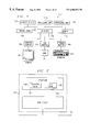
- FIG. 1 is a block diagram depicting the basic structure of a conventional multiprocessor computer system
- FIG. 2 is a block diagram depicting a typical architecture
- FIG. 3 is a block diagram depicting an SMP computer system with three processing units
- FIG. 4 is a block diagram depicting a distributed system structure for a symmetric multiprocessor system with supporting bus-based cache-coherence protocol from the perspective of address paths within the SMP system;
- FIG. 5 is a block diagram depicting a distributed system structure for a symmetric multiprocessor system with supporting bus-based cache-coherence protocol from the perspective of data paths within the SMP system;
- FIG. 6 is a block diagram depicting the address paths internal to a node controller
- FIG. 7 is a diagram depicting the internal address paths of an address switch connecting node controllers and memory subsystems
- FIG. 8 is a diagram depicting a memory subsystem connected to the address switch of the distributed system of the present invention.
- FIGS. 9A-B are a block diagram depicting the data paths internal to a node controller
- FIGS. 10A-10B are block diagrams depicting the system structure for determining bus response signals for a distributed system structure
- FIGS. 10C-10D are block diagrams depicting the components whose signals participate in the local and global cycles C
- FIGS. 11A-B are a block diagram depicting the relationship between multiple processors having multiple interrupt handlers and multiple interrupt distribution units within a large-way, distributed multiprocessor system in accordance with a preferred embodiment of the present invention.
- FIG. 12 is a block diagram depicting a centralized interrupt arbiter in accordance with a preferred embodiment of the present invention.
- Computer system 110 has several processing units 112 a , 112 b , and 112 c which are connected to various peripheral devices, including input/output (I/O) agents 114 , which accept data from and provide data to a monitor adapter 102 and display monitor 105 , keyboard adapter 104 and keyboard 107 , and disk adapter 103 and permanent storage device 106 , memory device 116 (such as dynamic random access memory or DRAM) that is used by the processing units to carry out program instructions, and firmware 118 whose primary purpose is to seek out and load an operating system from one of the peripherals (usually the permanent memory device) whenever the computer is first turned on.
- I/O agents 114 which accept data from and provide data to a monitor adapter 102 and display monitor 105 , keyboard adapter 104 and keyboard 107 , and disk adapter 103 and permanent storage device 106
- memory device 116 such as dynamic random access memory or DRAM
- firmware 118 whose primary purpose is to seek out and load an operating system from one of the peripherals (usually
- Processing units 112 a - 112 c communicate with the peripheral devices by various means, including a bus 120 .
- Computer system 110 may have many additional components which are not shown, such as serial and parallel ports for connection to peripheral devices, such as modems or printers. Those skilled in the art will further appreciate that there are other components that might be used in conjunction with those shown in the block diagram of FIG. 1; for example, a display adapter might be used to control a video display monitor, a memory controller can be used to access memory 116 , etc.
- computer system 110 may be configured with more or fewer processors.
- SMP symmetric multiprocessor
- a processing unit 112 includes a processor 122 having a plurality of registers and execution units, which carry out program instructions in order to operate the computer.
- the processor can also have caches, such as an instruction cache 124 and a data cache 126 . These caches are referred to as “on-board” when they are integrally packaged with the processor's registers and execution units. Caches are commonly used to temporarily store values that might be repeatedly accessed by a processor, in order to speed up processing by avoiding the longer step of loading the values from memory, such as memory 116 shown in FIG. 1 .
- Processing unit 112 can include additional caches, such as cache 128 .
- Cache 128 is referred to as a level 2 (L2) cache since it supports the on-board (level 1) caches 124 and 126 .
- L2 level 2
- cache 128 acts as an intermediary between memory 116 and the on-board caches, and can store a much larger amount of information (instructions and data) than the on-board caches, although at a longer access penalty.
- cache 128 may be a chip having a storage capacity of 256 or 512 kilobytes
- the processor 112 may be an IBM PowerPCTM 604-series processor having on-board caches with 64 kilobytes of total storage.
- Cache 128 is connected to bus 120 , and all loading of information from memory 116 into processor 112 must come through cache 128 .
- FIG. 2 depicts only a two-level cache hierarchy, multi-level cache hierarchies can be provided where there are many levels of serially connected caches.
- an SMP computer system is depicted with three processing units ( 140 , 141 , 142 ) consisting of processors ( 140 a , 141 a , 142 a ) each having an L1 cache ( 140 b , 141 b , 142 b ), and L2 cache ( 140 c , 141 c , 142 c ), and finally, an L3 cache ( 140 d , 141 d , 142 d ).
- each lower-level cache i.e., an L3 cache is “lower” than an L2
- each lower-level cache i.e., an L3 cache is “lower” than an L2
- each lower-level cache i.e., an L3 cache is “lower” than an L2
- L3 cache is typically larger in size and has a longer access time than the next higher-level cache.
- the lower-level caches contain copies of all blocks present in the higher-level caches.
- the L2 cache of a given processing unit that implies the L3 cache for that processing unit also has a (potentially stale) copy of the block.
- a block is present in the L1 cache of a given processing unit, it is also present in the L2 and L3 caches of that processing unit.
- This property is known as inclusion and is well-known to those skilled in the art. Henceforth, it is assumed that the principle of inclusion applies to the cache related to the present invention.
- the processors communicate over a common generalized interconnect ( 143 ).
- the processors pass messages over the interconnect indicating their desire to read or write memory locations.
- all of the other processors “snoop” this operation and decide if the state of their caches can allow the requested operation to proceed and, if so, under what conditions. This communication is necessary because, in systems with caches, the most recent valid copy of a given block of memory may have moved from the system memory 144 to one or more of the caches in the system.
- the correct version of the block which contains the actual value for the memory location, may either be in the system memory 144 or in one of the caches in processing units 141 and 142 . If the correct version is in one of the other caches in the system, it is necessary to obtain the correct value from the cache in the system instead of system memory.
- a processor say 140 a attempting to read a location in memory. It first polls its own L1 cache ( 140 b ). If the block is not present in the L1 cache ( 140 b ), the request is forwarded to the L2 cache ( 140 c ). If the block is not present in the L2 cache, the request is forwarded on to the L3 cache ( 140 d ). If the block is not present in the L3 cache ( 140 d ), the request is then presented on the generalized interconnect ( 143 ) to be serviced. Once an operation has been placed on the generalized interconnect, all other processing units “snoop” the operation and determine if the block is present in their caches.
- a given processing unit say 142
- the L2 cache ( 142 c ) and the L3 cache ( 142 d ) also have copies of the block. Therefore, when the L3 cache ( 142 d ) of processing unit 142 snoops the read operation, it will determine that the block requested is present and modified in the L3 cache ( 142 d ).
- the L3 cache ( 142 d ) may place a message on the generalized interconnect informing processing unit 140 that it must “retry” its operation again at a later time because the most recently updated value of the memory location for the read operation is in the L3 cache ( 142 d ), which is outside of main memory 144 , and actions must be taken to make it available to service the read request of processing unit 140 .
- the L3 cache ( 142 d ) may begin a process to push the modified data from the L3 cache to main memory 144 .
- the most recently updated value for the memory location has then been made available to the other processors.
- the L3 cache ( 142 d ) may send the most recently updated value for the memory location directly to processing unit 140 , which requested it.
- the L3 cache may then begin a process to push the modified data from the L3 cache to main memory.
- Processing unit 140 specifically its L3 cache ( 140 d ), eventually represents the read request on the generalized interconnect. At this point, however, the modified data has been retrieved from the L1 cache of processing unit 142 and the read request from processor 140 will be satisfied.
- a read request is snooped on the generalized interconnect which causes processing unit 142 to “push” the block to the bottom of the hierarchy to satisfy the read request made by processing unit 140 .
- the cache-coherence protocol associates, with each block in each level of the cache hierarchy, a status indicator indicating the current “state” of the block.
- the state information is used to allow certain optimizations in the coherency protocol that reduce message traffic on generalized interconnect 143 and inter-cache connections 140 x , 140 y , 141 x , 141 y , 142 x , 142 y .
- this mechanism when a processing unit executes a read, it receives a message indicating whether or not the read must be retried later.
- the message usually also includes information allowing the processing unit to determine if any other processing unit also has a still active copy of the block (this is accomplished by having the other lowest-level caches give a “shared” or “not shared” indication for any read they do not retry).
- a processing unit can determine whether any other processor in the system has a copy of the block. If no other processing unit has an active copy of the block, the reading processing unit marks the state of the block as “exclusive.” If a block is marked exclusive, it is permissible to allow the processing unit to later write the block without first communicating with other processing units in the system because no other processing unit has a copy of the block. Therefore, in general, it is possible for a processor to read or write a location without first communicating this intention onto the interconnection. However, this only occurs in cases where the coherency protocol has ensured that no other processor has an interest in the block.
- a set is the collection of blocks in which a given memory block can reside. For any given memory block, there is a unique set in the cache that the block can be mapped into, according to preset mapping functions.
- the number of blocks in a set is referred to as the associativity of the cache (e.g., 2-way set associative means that, for any given memory block, there are two blocks in the cache that the memory block can be mapped into). However, several different blocks in main memory can be mapped to any given set.
- the cache When all of the blocks in a set for a given cache are full and that cache receives a request, whether a read or write, to a memory location that maps into the full set, the cache must “deallocate” one of the blocks currently in the set.
- the cache chooses a block to be evicted by one of a number of means known to those skilled in the art (least recently used (LRU), random, pseudo-LRU, etc.). If the data in the chosen block is modified, that data is written to the next lowest level in the memory hierarchy, which may be another cache (in the case of the L1 or L2 cache) or main memory (in the case of an L3 cache). Note that, by the principle of inclusion, the lower level of the hierarchy will already have a block available to hold the written modified data.
- LRU least recently used
- the block is simply abandoned and not written to the next lowest level in the hierarchy.
- This process of removing a block from one level of the hierarchy is known as an “eviction.”
- the cache no longer holds a copy of the evicted block and no longer actively participates in the coherency protocol for the evicted block because, when the cache snoops an operation (either on generalized interconnect 143 or inter-cache connections 140 x , 141 x , 142 x , 140 y , 141 y , 142 y ), the block will not be found in the cache.
- the present invention discloses a distributed hardware structure to overcome the limitations of a single common bus in a multiprocessor system while utilizing the properties of the single bus so that it does not require a modification to the bus protocol.
- the resulting system has a scalable system size without compromising the mechanism of a known system bus.
- the present invention is able to connect together a large number of devices in an SMP system and overcome the limitations of a single-bus-based design.
- FIG. 4 a block diagram depicts a distributed system structure for a symmetric multiprocessor system with supporting bus-based cache-coherence protocol from the perspective of address paths within the SMP system.
- FIG. 4 displays a number of master devices that can initiate a command, such as a memory transaction.
- master devices such as processors, I/O agents, and coherent memory adapters, are distributed in clusters among a number of N groups called nodes. Each node is headed by a node controller into which its masters connect.
- FIG. 4 shows nodes 410 and 420 , which contain groupings of system elements.
- the number of nodes may vary based on the configuration of the system.
- Node 410 also labeled as Node 0
- processors 411 and 412 also labeled as Processor P 0 and Processor P p ⁇ 1 , which are the masters for Node 410 .
- Each node controller has multiple standard bidirectional processor address-data buses over which masters are connected into the distributed system.
- Processors 411 and 412 connect to node controller 415 , also labeled as Node Controller NC 0 , via buses 413 and 414 , also labeled as P 0 Bus and P p ⁇ 1 Bus, respectively.
- Node 420 also labeled as Node N ⁇ 1 , contains processor 421 and I/O agent 422 , which are the masters for Node 420 .
- Processor 421 and I/O device 422 connect to node controller 425 , also labeled as Node Controller NC N ⁇ 1 via buses 423 and 424 , respectively.
- the number of masters per node may vary depending upon the configuration of the system, and the number of masters at each node is not required to be uniform across all of the nodes in the system.
- the node controller constitutes the physical interface between a master and the rest of the system, and each node controller in the system contains all of the necessary logic to arbitrate for individual processor buses and to communicate with its local masters as another master or as a slave, i.e. a device that accepts master commands and executes them but does not generate master commands.
- a processor sends a command into the system via its local node controller.
- FIG. 4 shows one master per port, multiple masters per port are possible given an appropriate arbitration scheme on the bus of that port.
- processor 411 could be one of many processors connected to bus 413 . However, if more processors are connected to a single port, then their address bus will perform more slowly in terms of bus cycle time.
- one of the masters of Node 420 may include a coherent memory adapter that provides communication with another data processing system that maintains cache coherence.
- the coherent memory adapter may be proximate or remote and may occupy a port of a node controller to send and receive memory transactions in order to behave as a master/slave device in a manner similar to an I/O agent.
- another node controller from another data processing system may also be connected to the coherent memory adapter so that data processing systems that employ the present invention may be chained together.
- Node controllers 415 and 425 are connected to a device called an address switch (ASX) via pairs of unidirectional address-only buses.
- Buses 416 and 417 also labeled AOut 0 and AIn 0 , respectively, connect node controller 415 to address switch 430 .
- Buses 426 and 427 also labeled AOut N ⁇ 1 and AIn N ⁇ 1 , respectively, connect node controller 425 to address switch 430 .
- buses AOut x carry addresses from the node controllers to the address switch
- buses AIn x carry addresses from the address switch to the node controllers.
- Address switch 430 has additional unidirectional address bus connections 431 and 432 , also labeled as AIn N and AIn (N+S ⁇ 1) , to memory controllers or memory subsystems 442 and 444 , also labeled as memory subsystem MS 0 and MS S ⁇ 1 .
- the memory controllers are assumed to be slave devices and have no ability to issue commands into the distributed system.
- the number of memory subsystems may vary depending upon the configuration of the system.
- FIG. 5 a block diagram depicts a distributed system structure for a symmetric multiprocessor system with supporting bus-based cache-coherence protocol from the perspective of data paths within the SMP system.
- FIG. 5 displays a number of master devices. These master devices are distributed in clusters among a number of N groups called nodes. Each node is headed by a node controller into which its masters connect.
- FIG. 5 shows nodes 510 and 520 containing processors 511 and 512 . Processors 511 and 512 connect to node controller 515 via buses 513 and 514 .
- Node 520 also labeled as Node N ⁇ 1 , contains processor 521 and I/O device 522 that connect to node controller 525 , also labeled as Node Controller NC N ⁇ 1 via buses 523 and 524 , respectively.
- FIG. 4 and FIG. 5 could be physically the same system component but are described from different perspectives to show different functionality performed by the node controllers.
- FIG. 4 shows address paths within the SMP system
- FIG. 5 shows the data paths within the SMP system.
- the address paths and data paths may be implemented with supporting functionality in physically separate components, chips, or circuitry, such as a node data controller or a node address controller.
- the choice of implementing a node controller with separate or combined data and address functionality may depend upon parameters of other system components. For example, if the sizes of the buses supported within the system are small enough, both address and data functionality may be placed within a single node controller component. However, if the buses support 128 bits of data, then pin limitations may physically require the address and data functionality to be placed within separate node controller components.
- a separate node data controller may be further separated into multiple node data controllers per node so that each node data controller provides support for a portion of the node's data path. In this manner, the node's data path is sliced across more than one node data controller.
- each node controller is shown connected to a plurality of memory controllers, such as memory subsystems MS 0 and MS S ⁇ 1 . Although each node controller is shown to connect to each memory controller via an independent data bus, multiple nodes and/or multiple memory controllers may be connected on the same data bus if an appropriate arbitration mechanism is included. As with connecting a plurality of master devices to a single node controller via a single bus, the switching rate will be a function of the number of devices connected to the bus.
- Node controller 515 connects to memory subsystem 542 via data bus 516 , and to memory subsystem 544 via bus 517 , also labeled as N 0 D 0 and N 0 D S ⁇ 1 , respectively.
- Node controller 525 connects to memory subsystem 544 via data bus 527 , and to memory subsystem 542 via data bus 526 , also labeled as N N ⁇ 1 D S ⁇ 1 , and N N ⁇ 1 D 0 , respectively.
- Node controller 600 also labeled NC x , is similar to node controllers 415 and 425 in FIG. 4 or node controllers 515 and 525 in FIG. 5 .
- Individual ports of node controller 600 have their own queues to buffer commands from masters as the commands enter the node controller. A command may incur non-deterministic delay while waiting in these buffers for progressive selection toward the address switch.
- Node controller 600 has bidirectional buses 601 - 604 that connect to master devices. Buses 601 - 604 connect to input boundary latches 609 - 612 and output boundary latches 613 - 616 via bus transceivers 605 - 608 . Input boundary latches 609 - 612 feed buffers 617 - 620 that hold the commands from the master devices.
- a command from a master device may consist of a transaction tag, transaction type, target or source address, and other possible related information.
- Buffers 617 - 620 may hold all information related to a command, if necessary, or may alternatively hold only the information necessary for the functioning of the address path within the node controller.
- Buffers 617 - 620 feed control unit/multiplexer 621 that selects one command at a time to send to the address switch via latch 622 , transmitter 623 , and bus 624 , also labeled AOut x .
- Node controller 600 receives commands from masters via buses 601 - 604 for eventual transmittal through boundary latch 622 and transmitter 623 to the address switch via bus 624 , also labeled bus AOut x .
- node controller 600 accepts commands from the address switch via bus 625 , also labeled bus AIn x , and receiver 626 for capture in boundary latch 627 , also labeled as FROM_ASX_BL. These commands follow an address path through a fixed number of latches that have a fixed delay, such as intermediate latch 628 and output boundary latches 613 - 616 , before reaching buses 601 - 604 .
- commands to master devices also pass through a multiplexer per port, such as control units/multiplexers 629 - 632 , that also have a fixed delay.
- commands arriving via bus 625 traverse a path with a fixed delay of a deterministic number of cycles along the path.
- a fixed period of time occurs between the point when a command reaches latch FROM_ASX_BL to the point at which each master device, such as a set of processors connected to the node controller, is presented with the arriving command.
- the arbiters for the ports connected to the masters are designed to give highest priority to the node controllers driving the port buses. If a master makes a request to drive a bus at the same time that the node controller expects to drive it, the node controller is given highest priority.
- a signal called “SnoopValid” (not shown) is asserted by the address switch ahead of the command being sent by the address switch. This allows the arbitration for the bus accesses between a node controller and its masters to be completed early enough to ensure that a command arriving from the address switch via the AIn x bus does not stall for even one cycle while inside the node controller.
- Control logic unit 633 is also presented with the incoming command latched into the FROM_ASX_BL latch for appropriate determination of control signals to other units or components within node controller 600 .
- Control logic unit 633 also receives other control signals 637 , as appropriate.
- FIG. 7 a diagram depicts the internal address paths of an address switch connecting node controllers and memory subsystems.
- Address switch 700 connects a set of four node controllers and two memory subsystems.
- Commands arrive at first-in first-out (FIFO) queues 721 - 724 from buses 701 - 704 , also labeled AOut 0 -AOut 3 , via receivers 709 - 712 and input boundary latches 713 - 716 .
- FIFO first-in first-out
- Control logic unit 726 may communicate with control unit/multiplexer 725 and FIFOs 721 - 724 in order to determine the selection of incoming commands.
- Control logic unit 726 also receives other control signals 733 , as appropriate.
- Control unit/multiplexer 725 selects one command at a time to be broadcast to the node controllers and memory subsystems over paths that are deterministic in terms of the number of cycles of delay.
- commands are sent to the memory subsystems via unidirectional buses 731 and 732 , also labeled as buses AIn 4 and AIn 5 , through output boundary latches 727 and 728 and transmitters 729 and 730 .
- Commands are sent to node controllers via unidirectional buses 705 - 708 , also labeled as buses AIn 0 -AIn 3 , through output boundary latches 711 - 720 and transmitters 741 - 744 .
- a transaction is issued by a master device via its bus and port to its node controller.
- the node controller will provide some type of immediate response to the master device via the bus and may queue the transaction for subsequent issuance to the rest of the system.
- the address switch ensures that the transaction can be broadcast to the rest of the system with a known propagation delay so that the other devices may snoop the transaction.
- each of the devices within the system would be able to see the transaction in the same cycle and provide a coherence response within the same cycle.
- the address switch is able to broadcast a transaction to all node controllers, including the node controller of the node containing the device that issued the transaction.
- Appropriate logic is embedded within each node controller so that a node controller may determine whether the incoming transaction being snooped was originally issued by a device on one of its ports. If so, then the node controller ensures that the bus on the port that issued the transaction is not snooped with a transaction that was received from that port. Otherwise, the device may get “confused” by being snooped with its own transaction.
- the device may issue a response indicating a collision with its original transaction. If that were the case, since the original transaction is actually the transaction that is being snooped, then the “collision” would never be resolved, and the transaction would never complete.
- FIG. 8 a diagram depicts a memory subsystem connected to the address switch of the distributed system of the present invention.
- FIG. 8 shows memory subsystem 800 , also labeled memory subsystem MS x .
- Memory controller 801 within memory subsystem 800 receives a command from the address switch via unidirectional bus 802 , also labeled as bus AIn x , through a number of latches FD 803 , which is merely a fixed delay pipe. In this manner, a command sent by the address switch experiences a fixed number of cycles of delay before the command is made available to the memory controller.
- a command arriving at a node controller via bus AIn x traverses a deterministic delay path from its capture in the FROM_ASX_BL latch to its presentation to a master device.
- a command traverses a deterministic delay path from the control unit/multiplexer within the address switch to the fixed delay pipe within the memory subsystem. If the delay of the latches FD 803 within the memory subsystem is adjusted to the appropriate value, it can be ensured that the memory controller is presented with a command at the same time that the masters connected to the ports of the node controllers are presented with the same command. Hence, there is a deterministic number of cycles between the point at which the control unit/multiplexer within the address switch broadcasts a transaction and the point at which the masters and memory controllers receive the command.
- the speed at which each bus is connected to these ports may be operated is independent of the total number of ports in the system. For example, if a single master is connected to each port, its bus can be run in point-to-point mode at the best possible speed.
- the distributed structure of the present invention is able to scale well-understood and easier-to-verify bus-based cache-coherent protocols for multiprocessors to enhance the bandwidth of the system.
- Node controller 900 also labeled NC x , is similar to node controllers 415 and 425 in FIG. 4 or node controllers 515 and 525 in FIG. 5 .
- Individual ports of node controller 900 have their own queues to buffer data from masters as data enters the node controller. Data may incur non-deterministic delay while waiting in these buffers for progressive movement toward destinations.
- Node controller 900 has bidirectional buses 901 - 904 , also labeled P x Bus, that connect to master devices. Buses 901 - 904 connect to input boundary latches 909 - 912 and output boundary latches 913 - 916 via bus transceivers 905 - 908 . Input boundary latches 909 - 912 feed data buffers 917 - 920 that hold the data from the master devices.
- Incoming data from one of the node controller's ports may be directed to a memory subsystem or another cache.
- incoming data from one of the node controller's ports may be directed to one of three locations: memory subsystem MS 0 , memory subsystem MS S ⁇ 1 , or a cache-to-cache FIFO (FIFO C2C) for forwarding data within the node.
- FIFO C2C cache-to-cache FIFO
- each node is able to transfer data from one of its ports to another port, thereby allowing the transfer of data from one master to another.
- Buffers 917 - 920 feed multiplexers 925 - 927 that select a data source for forwarding data.
- Control logic unit 939 provides control signals for multiplexer 925 to select data to be sent to memory subsystem MS 0 and for multiplexer 926 to select data to be sent to memory subsystem MS S ⁇ 1 .
- Node controller 900 sends data from multiplexers 925 and 926 through boundary latches 931 and 933 and transceivers 935 and 936 to memory subsystem MS 0 and memory subsystem MS S ⁇ 1 via bidirectional buses 937 and 938 , also labeled N x D 0 and N x D S ⁇ 1 .
- Control logic unit 939 provides control signals for multiplexer 927 to select data to be forwarded within the node. Data is then queued into FIFO 928 .
- node controller 900 accepts data through transceivers 935 and 936 and boundary latches 932 and 934 from memory subsystem MS 0 and memory subsystem MS ⁇ 1 via bidirectional buses 937 and 938 . Data is then queued into appropriate FIFOs 929 and 930 . Data from FIFOs 928 - 930 pass through a multiplexer per port, such as control units/multiplexers 921 - 924 . Control logic unit 939 provides control signals for multiplexers 921 - 924 to select data to be sent to the master devices. Control logic unit 939 also receives other control signals 940 , as appropriate. Hence, the node controller has arbitration logic for data buses and is self-sufficient in terms of controlling the data transfers with parallelism. In this manner, the distributed system structure of the present invention is able to improve system data throughput.
- FIGS. 10A-10B block diagrams depict the system structure for determining bus response signals for a distributed system structure similar to that shown in FIG. 4 and FIG. 5 .
- FIG. 10 A and FIG. 10B show the connectivities of devices in the distributed system structure of the present invention with a control logic block for combining bus signals (responses) AStat and AResp, respectively.
- AStat signals and AResp signals have been shown separately.
- I/O agents may act as master devices connected to the ports of the node controllers shown in FIG. 10 A and FIG. 10 B.
- processors 1001 - 1004 also labeled P x
- have unidirectional AStatOut signals 1005 - 1008 also labeled P x N x AStOut
- AStatIn signals 1009 - 1012 also labeled P x N x AStIn, connecting the processors to Response Combination Block (RCB) 1000 .
- the slave devices such as memory subsystems 1005 and 1006 , also labeled MS x , connect to the RCB with AStatOut signals 1013 and 1014 , also labeled M x— AStOut, and with AStatIn signals 1015 and 1016 , also labeled M x— AStIn.
- Node controllers 1017 and 1018 also labeled NC x also connect to the RCB via a similar set of per port unidirectional AStatOut signals 1019 - 1022 , also labeled N x P x AStOut, and AStatIn signals 1023 - 1026 , also labeled N x P,AStIn.
- Address switch 1027 also labeled ASX, participates in determining the proper logic for system processing of a transaction by supplying broadcast signal 1028 and transaction source ID 1029 , which is an encoding of a node identifier together with a port identifier within the node through which a master device issued a transaction to the system.
- processors 1001 - 1004 have unidirectional ARespOut signals 1055 - 1058 , also labeled P x N x AReOut, and ARespIn signals 1059 - 1062 , also labeled P x N x AReIn, connecting the processors to RCB 1000 .
- Memory subsystems 1005 and 1006 connect to the RCB with ARespIn signals 1065 and 1066 , also labeled M x— AReIn.
- Memory subsystems 1005 and 1006 do not connect with ARespOut lines, which are not driven by these slave devices.
- Node controllers 1017 and 1018 also connect to the RCB via a similar set of per port unidirectional ARespOut signals 1069 - 1072 , also labeled N x P x AReOut, and ARespIn signals 1073 - 1076 , also labeled N x P x AReIn.
- address switch 1027 participates in determining the proper logic of a transaction by supplying broadcast signal 1078 and transaction port ID 1079 .
- RCB 1000 supplies a HOLDTAG signal, such as signals 1091 and 1092 , to each node controller in certain circumstances, as explained further below.
- a set of AStatIn/AStatOut signals and ARespIn/ARespOut signals to/from a master device is paired with a similar set of AStatIn/AStatOut signals and ARespIn/ARespout signals to/from its node controller.
- This pairing is done on a per port basis.
- each port in the example is shown with a single master device connected to each port. However, if more than one master device were connected per port, then the pairs of AStatIn/AStatOut signals and ARespIn/ARespOut signals are used by the set of master devices connected to the bus on that port as in a standard single bus configuration.
- RCB combines the AStatOuts and ARespOuts from various source devices and produces AStatIn and ARespIn signals per the 6XX bus specification, as described in IBM Server Group Power PC MP System Bus Description, Version 5.3, herein incorporated by reference.
- the RCB receives the AStatOuts and ARespOuts signals and returns AStatIns and ARespIns, respectively. Not all of the devices receive the same responses for a particular transaction.
- the signals received by each device are determined on a per cycle basis as described in more detail further below.
- a master device at a port may be issuing a transaction over its port's bus for receipt by its node controller or the node controller may be presenting the master device with a transaction forwarded by the address switch in order to snoop the transaction.
- the cycle is labeled “local,” and when the node controller is presenting a transaction, the cycle is labeled “global.”
- the address switch broadcasts one transaction at a time to all of the node controllers, and there is a fixed delay between the time the address switch issues such a transaction and the time it appears at the ports of each node controller.
- a node controller has received a broadcast transaction from the address switch and then, a predetermined number of cycles later, is presenting the transaction to the devices on the buses of the ports of the node controller during a cycle, all node controllers are performing the same action on all of their ports during the same cycle, except for one exception, as explained below.
- global cycles are being executed on all the ports in the system. All remaining cycles are local cycles.
- a global cycle occurs when a transaction is being snooped by all the devices in the system, and only a local cycle may be used by a device to issue a transaction.
- the response generation, the response combination, and the response reception cycles which occur after a fixed number of cycles subsequent to the issuance of a transaction, are similarly labeled local response windows or global response windows.
- the RCB's response combination function is correspondingly considered to be in either local or global mode during a given cycle.
- the RCB combines responses on a per port basis. That is, the RCB combines the response of a port and the response that the node controller produces corresponding to that port.
- the RCB combines responses from all the ports and node controllers in the system (again, except for one port, as explained below).
- the RCB is provided with a signal indicating the broadcast of a transaction by the address switch to the node controllers, shown as broadcast signal 1028 in FIG. 10A, as well as the transaction source ID signal 1029 .
- Configuration information stored in the RCB indicates the exact cycle in which the combination of responses is to be performed for the broadcast transaction after the arrival of the broadcast transaction signal. In this manner, for each global cycle, the RCB is orchestrated to combine responses from appropriate sources.
- a processor may issue a transaction only during local cycles. For certain types of transactions, the processor issues the transaction only once. For certain other types of transactions, the processor might be required to issue the transaction multiple times.
- the processor is directed by its node controller, in conjunction with the RCB, through the use of the AStatIn/AStatOut signals and the ARespIn/ARespOut signals as to the actions that should be performed.
- the local cycles in which a processor issues transactions for the first time are labeled “primary local cycles” whereas all other local cycles are labeled “secondary local cycles”.
- a secondary transaction is marked by the “R” bit being set to “1”. In other words, its response-related cycles get labeled primary or secondary in the proper manner corresponding to the transaction issuance.
- processors and devices see transactions from other processors and devices during cycles different than the cycle in which are issued to the system. This is unlike the situation with a snooping protocol in a single bus environment in which all the devices in the system observe a transaction at the same time that it is issued and simultaneously produce a coherence response for it and in which the originator of the transaction receives the response at that same time.
- the achievement of coherence is both distributed in time and distributed in space, i.e. across multiple cycles and multiple buses connected to multiple node controllers.
- the node controller accepts the transaction and issues a global coherence response to the issuing entity in the primary response window.
- the node controller then takes full responsibility of completing the transaction in the system at a later time and achieving the global response.
- the node controller takes three steps. First, the node controller accepts the transaction and delivers a primary response that indicates postponement of achievement and delivery of the global response. In the 6XX bus architecture, this response is the “Rerun” response. Second, at a subsequent time, the node controller achieves a global coherence response for that transaction. And third, the node controller requests that the processor issue a secondary transaction and delivers the global response in the secondary response window. In the 6XX bus architecture, the request to the processor to issue a secondary transaction is made by issuing it a Rerun command with a tag corresponding to the original transaction. The processor may then use the tag to identify which of its transactions should be rerun.
- a transaction accepted from a device is snooped to the rest of the system.
- the device that issued the transaction is not snooped so that the device does not get confused by being snooped with its own transaction.
- the port corresponding to the device that issued the transaction is kept in the local mode in the transaction's snoop cycle so that the processor may issue another transaction.
- the RCB is configured to combine responses from all sources other than the port on the node controller that issued the transaction. The node controller is then able to supply a primary or secondary response over that port if the processor chooses to issue a transaction.
- the node controller keeps the particular port in local mode but issues it a Rerun transaction.
- the control unit/multiplexer feeding the outgoing boundary latch at the port allows the node controller to achieve this functionality.
- the node controller may choose to not be as aggressive, and instead of letting the device issue a transaction, the node controller might itself issue a null or rerun transaction, as required, to the device in the cycle during which the device's transaction is being snooped in the rest of the system.
- FIG. 10C shows the signals which are considered by the RCB during a global cycle.
- the signals for a single master device, processor 1001 do not participate in the determination by the RCB of the appropriate signals to the other devices, node controllers, and memory subsystems for the global response.
- the signals for processor 1001 are paired with the corresponding signals from its node controller, which are also not considered for the global response. From the perspective of processor 1001 , it is kept in a local cycle while a transaction issued by processor 1001 is snooped by the rest of the system.
- the signals are considered on a per port basis, and the bus of a particular port is kept in a local cycle while the rest of the system is in a global cycle.
- FIG. 10D shows the signals which are considered by the RCB during a local cycle.
- the signals from a single master device, processor 1001 participate in the determination by the RCB of the appropriate signals to be returned to processor 1001 and its node controller. Signals from the other devices, node controllers, and memory subsystems may be simultaneously participating in the response for the global response.
- the signals for processor 1001 are paired with the corresponding signals from its node controller, which also do not affect the global response. From the perspective of processor 1001 , it may issue another transaction while its other transaction is snooped by the rest of the system. For the sake of clarity, signals from the address switch are not shown for the local cycle, although the RCB uses these signals to determine which port to place into the local cycle.
- devices in an SMP system access memory, either under the influence of programs or control sequences, they issue memory transactions.
- the devices may also issue other bus transactions to achieve coherence, ordering, interrupts, etc., in the system. These transactions can usually complete in parallel without interference from other transactions.
- two transactions refer to addresses within the same double word, for example, they are said to have “collided,” according to the 6XX bus terminology, and the two transactions must be completed in some specific order. In some cases, either completion order is acceptable, and at other times, the order is fixed and is implied by the types of transactions. For instance, if a read transaction and a Write transaction attempt to access an address declared as Memory Coherence Not Required, any order of completion for the two transactions is acceptable. However, if they refer to a cachable address to be maintained coherent, the order of completion must appear to be the write followed by the read.
- Node controllers send one of the registered transactions at a time to the address switch.
- the address switch chooses one transaction at a time with a fair arbitration among the transactions sent to it and then broadcasts the chosen transaction back to the node controllers and to the memory subsystems.
- the address portion of the transaction broadcast by the address switch is first latched inside the node controller in the boundary latch FROM_ASX_BL.
- a transaction arrives in FROM_ASX_BL for the first time, it is marked as being “snooped,” to indicate the fact that in a fixed number of cycles following the current cycle, the transaction will be presented for snooping, for the first time, to all the devices in the system.
- the following rule is used to assign a transaction its relative position in the order of transactions to be completed, irrespective of the actual time it entered the system: a registered transaction that already is marked as snooped is nominally defined to have entered the system earlier than the current transaction in FROM_ASX_BL. The ones that have not been marked as snooped are nominally defined to have entered the system later than the current transaction in FROM_ASX_BL.
- the transaction in FROM_ASX_BL stays there for one cycle. During that cycle, the transaction is compared with every transaction currently registered in the entire system for detection of collision and ordering decision. There could be two sets of results of each of these pairwise comparisons: one that affects the completion of the transaction currently in FROM_ASX_BL and the second that affects the completion of some other transaction.
- Each comparison results in a decision to either allow the current presentation of the transaction in FROM_ASX_BL for snooping to complete, or to postpone its completion to a later time.
- the postponement is effected via the computation of an AStat Retry signal or an AResp Retry signal, as is appropriate.
- the combined AStat Retry and AResp Retry signals are encoded by the node controller into the AStat Retry and ARespRetry codes and are submitted to the RCB for participation in the global AStat and AResp windows of the transaction being snooped. During these windows, responses from all the devices, other than the device that issued the transaction, and node controllers are combined by the RCB to produce a global response which is returned to all the participants, as explained with respect to FIGS. 10A-10D above. Again, at this global level, a retry response has the highest priority (barring an error code) and will be the final response if any of the input responses was a retry.
- the effect of a global retry response is cancellation of the current snoop of the transaction.
- the node controller in which the transaction is registered either reissues the transaction for global snoop or retires the original transaction from which the said transaction was derived.
- a transaction receives a retry response, its snooped marking is reset, and it thus loses its present nominal position in the transaction order in the system. When it returns for snoop, the transaction gets a new position, according to the rule above.
- the mechanism does not necessarily prohibit the possibility of the reissued transaction being ordered behind another transaction that entered the system after it. If, on the other hand, the current transaction completes, it may cause other transactions to get retried.
- the node controller constitutes the physical interface between a master and the rest of the system, and each node controller in the system contains all of the necessary logic to arbitrate for individual processor buses and to communicate with its local masters as another master or as a slave, i.e. a device that accepts master commands and executes them but does not generate master commands.
- a processor sends a command into the system via its local node controller, which then queues the commands and assumes responsibility for completing the commands in some form.
- interrupt processing between an interrupt handler, a node controller, and an interrupt distribution unit in which an interrupt arbiter is located within a node controller.
- the discussion of the interrupt processing can be generalized by noting that the operations of interrupt arbiter, at least from the perspective of coordinating the distribution of interrupts, may be implemented either as a stand-alone device or implemented within each interrupt distribution unit.
- the interrupt arbiter may be a physically separate component with appropriate connections to other physical components. This observation both simplifies the following discussions and generalizes the present invention as operational modes between an interrupt arbiter and interrupt distribution units.
- interrupt handlers may be available and even necessary for the processing needs of the system, which may give rise to the need for multiple interrupt distribution devices in the system.
- each interrupt distribution device may be designed such that it is unaware of the presence of other interrupt distribution units in the system.
- a commerically available, off-the-shelf interrupt distribution unit may be designed in such a way that it is assumed that only a single interrupt distribution unit would be used within a given system.
- the following discussion describes a manner of fairly distributing the interrupts to multiple interrupt handlers so that multiple interrupt distribution devices may be employed in the system, if necessary, without collisions between the interrupt distribution devices in the selection of an interrupt handler for servicing an interrupt.
- the solution provided by the present invention allows commerically available interrupt distribution devices to be employed within the large-way, distributed multiprocessor system as described in FIGS. 4-10D.
- the interrupt arbitration scheme described herein below has particular advantages in a manner similar to utilizing the properties of a commercially available single bus so that the large-way, distributed multiprocessor system does not require a modification to a known bus protocol.
- commerically available interrupt distribution devices may be employed within the large-way, distributed multiprocessor system without modification, if desired.
- a device may issue an interrupt which could be serviced by multiple interrupt handlers. All of those interrupt handlers' interrupt lines may not be connected to a single interrupt distribution unit. Instead, they might be connected to multiple interrupt distribution units. Without coordination amongst them, each would independently pick a different interrupt handler to service the interrupt. However, only one can actually service the interrupt.
- the present invention describes a method by which an interrupt arbiter will fairly pick a single interrupt distribution unit to actually select the final interrupt handler. The present invention does not require additional sideband signals on the bus. It may be implemented as either a stand-alone device, or it can be integrated into each interrupt distribution unit.
- a centralized interrupt arbiter will pick a single interrupt distribution unit to service an interrupt if more than one of them could service it. Without the centralized interrupt arbiter, each interrupt distribution unit would pick an interrupt handler to service the interrupt, leading to chaos in the system.
- the need for the present invention arises when there are multiple interrupt distribution units on a single logical address bus that are not capable of arbitrating amongst themselves when more than one of them could choose an interrupt handler to service an interrupt.
- the present invention utilizes a round robin scheme to choose from among the eligible interrupt distribution units for any given interrupt. Those eligible are subject to change from interrupt to interrupt. These eligible interrupt distribution units are indicated by architected bits defined in the address portion of the request. The address bits are then altered prior to snooping to allow only the chosen interrupt distribution unit to service the interrupt. Altering address bits rather than sending a specific signal to a chosen interrupt distribution unit communicates the arbitration choice to it and obviates the need for additional sideband signals.
- the individual interrupt distribution units remain completely oblivious to the presence of other interrupt distribution units in the system and need not be redesigned from their original purpose to support this scheme.
- the present invention could also be embedded in each individual distribution unit to eliminate the need for an external arbiter device.
- the specific invention involves adding logic to a node controller chip to intercept all incoming interrupt transactions and alter them if necessary before being snooped.
- the architected bits within the address which define which interrupt handlers may service this interrupt are compared against which interrupt distribution units are associated with those eligible interrupt handlers. This is done with a simple masking (bitwise ANDing) of the architected address bits with configuration registers defining the interrupt distribution unit/interrupt handler relationships. There is one register defined for each interrupt distribution unit. The registers have a single bit for each interrupt handler in the system. The bit is set if that interrupt handler's interrupt line is attached to that interrupt distribution unit.
- the present invention actually alters the address bits of the transaction before it is snooped to the interrupt distribution units. Because the node controller temporarily stores all transactions in a queue prior to snooping, there is time to perform this selection and alteration in a single logical address bus. Another advantage of this invention is that only the node controller needs to be modified to implement this invention.
- the interrupt distribution units can be used as originally designed for fewer interrupt handlers than are present in the system.
- FIG. 11 a block diagram depicts the relationship between multiple processors having multiple interrupt handlers and multiple interrupt distribution units within a large-way, distributed multiprocessor system in accordance with a preferred embodiment of the present invention.
- FIG. 11 shows a similar organization of components with additional detail for interrupt arbitration.
- Node 1100 also labeled as Node 0 , contains processors 1101 - 1104 , also labeled as Processor P 0 through Processor P 3 , which are the masters for Node 1100 .
- Each node controller has multiple standard bidirectional processor address-data buses over which masters are connected into the distributed system.
- Processors 1101 - 1104 connect to node controller 1105 , also labeled as Node Controller NC 0 , via buses 1106 - 1109 , respectively.
- Node 1110 also labeled as Node 1 , contains I/O agents 1111 and 1112 , also labeled as I/O Agent IO 0 and IO 1 , which are the masters for Node 1110 .
- I/O devices 1116 provide I/O functionality via I/O agent 1111 , and I/O devices 1116 provide I/O functionality via I/O agent 1112 .
- I/O agents 1111 and 1112 connect to node controller 1113 , also labeled as Node Controller NC 1 , via buses 1114 and 1115 , respectively.
- Processors 1101 - 1104 contain interrupt vector tables 1121 - 1124 , respectively, for determining interrupt handlers for servicing interrupts received from I/O agents 1111 and 1112 .
- I/O agents 1111 and 1112 contain interrupt distribution units 1125 and 1126 for selecting an interrupt handler among the interrupt handlers connected to I/O agents 1111 and 1112 .
- interrupt handlers 0 - 7 for processor 1101 are tied to interrupt distribution unit 1125 via signals 1130 .
- Interrupt handlers 6 and 7 of processor 1102 are tied to interrupt distribution unit 1125 via signals 1131 , while interrupt handlers 0 - 5 of processor 1102 are tied to interrupt distribution unit 1126 via signals 1132 .
- Interrupt handlers 6 and 7 of processor 1103 are tied to interrupt distribution unit 1125 via signals 1133 , while interrupt handlers 0 - 5 of processor 1103 are tied to interrupt distribution unit 1126 via signals 1134 .
- Interrupt handlers 4 - 7 of processor 1104 are tied to interrupt distribution unit 1125 via signals 1135 , while interrupt handlers 0 - 3 of processor 1104 are tied to interrupt distribution unit 1126 via signals 1136 .
- Node controller 1105 contains Interrupt Distribution Configuration Registers (IDCRs) 1141 - 1144 , also labeled as IDCR 0 through IDCR 3 .
- An individual IDCR contains a set of registers. Each register in a IDCR set of registers is associated with an interrupt distribution unit, and each bit in the register represents a connection to from a particular interrupt handler to the interrupt distribution unit associated with the register.
- node controller 1113 contains IDCRs 1151 - 1154 , also labeled as IDCR 0 through IDCR 3 .
- the manner in which the IDCRs are configured may vary depending upon the implementation. As just two examples, the IDCRs may be configured at bootup time through a JTAG interface, or they may be memory mapped registers.
- FIG. 12 a block diagram depicts a centralized interrupt arbiter in accordance with a preferred embodiment of the present invention.
- the centralized arbiter provides for a two-level arbitration scheme.
- the centralized arbiter may be used for selecting eligible interrupt distribution units. Once an interrupt distribution unit is selected to distribute an interrupt, the interrupt distribution unit then selects an interrupt handler to service the interrupt.
- the interrupt arbitration scheme of the present invention is applicable to a single wired address bus with no node controllers if the interrupt arbitration scheme is embedded in each interrupt distribution unit to intercept outgoing addresses before they are put on the bus for snooping.
- the interrupt distribution units must then be modified, unlike a node-controller-based implementation as described above.
- Interrupt arbiter 1200 is a per-port interrupt arbiter. Each port in a node controller has an associated interrupt arbiter.
- Incoming transaction 1202 is received through a port of a node controller.
- the transaction may be copied from the input boundary latch.
- the address bits of the incoming transaction 1202 are masked with all of the IDCR registers associated with the input port by AND gates 1204 and 1206 .
- Each mask value stored in one of the registers in the IDCR register set is associated with a particular interrupt distribution unit (IDU).
- IDU interrupt distribution unit
- each IDCR has two registers and therefore two IDU masks, labeled IDU 0 mask 1208 and IDU 3 mask 1210 , supporting four IDUs.
- the number of registers or supportable IDUs may vary depending upon the system implementation. For example, if there are four ports on a node controller, and an IDU may be connected to each port, then each interrupt arbiter would require four registers in the register set of each IDCR.
- an interrupt handler on the port associated with interrupt arbiter 1200 may be selected by the IDU that is associated with an IDU mask, the corresponding bit in the IDU mask is set to provide an indication of the association of the interrupt handler with the IDU.
- Masked values 1212 and 1214 are input into OR gates 1216 and 1218 to determine whether a particular interrupt handler may be selected for this transaction, i.e. to determine whether the masked value has any bits that are set to indicate that there is an association between an interrupt handler on the given port and a particular IDU.
- OR gate outputs 1220 and 1222 are then provided to round-robin arbitration logic 1224 .
- round-robin arbitration logic 1224 generates two-bit output 1226 to select one of the four IDUs for the second-level arbitration for selecting a particular interrupt handler.
- Output 1226 provides selection control to multiplexer 1228 that selects among the masked transactions associated with the IDUs.
- the masked value represents modified incoming transaction 1230 with its address bits modified. Modified incoming transaction 1230 is then placed into the node controller's input queue for the associated input port prior to snooping.
- a state machine keeps track of the previous interrupt distribution unit that was chosen to service an interrupt. It then chooses the next highest numbered interrupt distribution unit eligible to service the next interrupt.
- interrupt distribution number 1 was chosen from among 0, 1, and 3 the previous time, and the current interrupt could be handled by 0 or 1, 0 will be chosen. If 0, 1, 2, and 3 had been eligible 2 would have been chosen, Wrapping back from 3 to 0 because 2 and 3 were not eligible can be seen in the first example.
- the number of interrupt distribution units could easily be expanded to more or decreased to fewer. There is also no requirement that the interrupt distribution units receive any dedicated arbitration signals from the node controller since communication with them is achieved via the altered address bits visible to all during the snoop cycle.
- This invention is implemented on each port of the node controller. Thus, if a node controller has four ports to attach four devices to, four instances of this invention are active simultaneously. They do not communicate with one another. They distribute interrupts coming only from the port they are associated with.
- the advantages of the present invention should be apparent in view of the detailed description provided above.
- the present invention allows scaling of standardized and easier-to-verify bus-based cache-coherence protocols to a large-way, multiprocessor system whose large size normally would make physical buses inefficient media for communication among system components, such as processors, memory subsystems, and I/O agents.
- system components such as processors, memory subsystems, and I/O agents.
- the present invention also allows component interfaces to be clocked faster than possible with a single bus, thereby enhancing the bandwidths of the component interfaces and resulting in higher total system bandwidth and performance.
- the present invention also supports multiple data buses, thereby multiplying the data bandwidth of the system and improving the efficiency of the processor.
- the data transfer parallelism of the present system also improves total system data throughput.
- Another advantage to this invention is that multiple interrupt distribution units can be made to work together in a single bus image to service interrupts for more interrupt handlers in that image than any one interrupt distribution unit could natively support. And it can be done without adding any additional signals between the arbiter and the interrupt distribution units.
- 32 interrupt handlers were desired in a single image, but only 16 could be supported by any one interrupt distribution unit, 2 or more interrupt distribution units could be used to service the 32 interrupt handlers if the present invention is implemented in the system.
- More interrupt distribution units could also be added to a 16 interrupt handler system if it is desired to distribute interrupt handling among multiple interrupt distribution units to spread out the system's interrupt handler selection process. Because each individual interrupt distribution unit has shared resources in high demand, spreading the selection of interrupt handlers to multiple devices will increase performance related to interrupts by decreasing the total demand on any one unit's resources.
Abstract
Description
Claims (20)
Priority Applications (1)
| Application Number | Priority Date | Filing Date | Title |
|---|---|---|---|
| US09/436,201 US6606676B1 (en) | 1999-11-08 | 1999-11-08 | Method and apparatus to distribute interrupts to multiple interrupt handlers in a distributed symmetric multiprocessor system |
Applications Claiming Priority (1)
| Application Number | Priority Date | Filing Date | Title |
|---|---|---|---|
| US09/436,201 US6606676B1 (en) | 1999-11-08 | 1999-11-08 | Method and apparatus to distribute interrupts to multiple interrupt handlers in a distributed symmetric multiprocessor system |
Publications (1)
| Publication Number | Publication Date |
|---|---|
| US6606676B1 true US6606676B1 (en) | 2003-08-12 |
Family
ID=27663372
Family Applications (1)
| Application Number | Title | Priority Date | Filing Date |
|---|---|---|---|
| US09/436,201 Expired - Lifetime US6606676B1 (en) | 1999-11-08 | 1999-11-08 | Method and apparatus to distribute interrupts to multiple interrupt handlers in a distributed symmetric multiprocessor system |
Country Status (1)
| Country | Link |
|---|---|
| US (1) | US6606676B1 (en) |
Cited By (52)
| Publication number | Priority date | Publication date | Assignee | Title |
|---|---|---|---|---|
| US20020133651A1 (en) * | 2001-03-19 | 2002-09-19 | Hsin-Min Wang | PCI extended function interface and PCI device using the same |
| US20030041232A1 (en) * | 2001-08-25 | 2003-02-27 | International Business Machines Corporation | Interruption handler-operating system dialog for operating system handling of hardware interruptions |
| US20030229742A1 (en) * | 2002-06-05 | 2003-12-11 | Moss Robert W. | Methods and structure for state preservation to improve fairness in bus arbitration |
| US20040024938A1 (en) * | 2002-08-02 | 2004-02-05 | Bian Qiyong B. | Flexible interrupt handling methods for optical networking apparatuses with multiple multi-protocol optical networking modules |
| US20040030819A1 (en) * | 2002-08-07 | 2004-02-12 | Emrys Williams | System and method for processing node interrupt status in a network |
| US20040111549A1 (en) * | 2002-12-10 | 2004-06-10 | Intel Corporation | Method, system, and program for improved interrupt processing |
| US6968411B2 (en) * | 2002-03-19 | 2005-11-22 | Intel Corporation | Interrupt processing apparatus, system, and method |
| US20060064296A1 (en) * | 2005-12-09 | 2006-03-23 | Devins Robert J | Method and system of design verification |
| US7051218B1 (en) | 2001-07-18 | 2006-05-23 | Advanced Micro Devices, Inc. | Message based power management |
| US20060136916A1 (en) * | 2004-12-17 | 2006-06-22 | Rowland John R | Method and apparatus for transaction performance and availability management based on program component monitor plugins and transaction performance monitors |
| US20060174169A1 (en) * | 2005-01-28 | 2006-08-03 | Sony Computer Entertainment Inc. | IO direct memory access system and method |
| US20060179247A1 (en) * | 2005-02-10 | 2006-08-10 | International Business Machines Corporation | Data processing system and method for efficient communication utilizing an Ig coherency state |
| US20060179252A1 (en) * | 2005-02-10 | 2006-08-10 | International Business Machines Corporation | Data processing system and method for efficient communication utilizing an In coherency state |
| US20060179249A1 (en) * | 2005-02-10 | 2006-08-10 | International Business Machines Corporation | Data processing system and method for predictively selecting a scope of broadcast of an operation utilizing a location of a memory |
| US20060179248A1 (en) * | 2005-02-10 | 2006-08-10 | International Business Machines Corporation | Data processing system and method for efficient storage of metadata in a system memory |
| US20060179245A1 (en) * | 2005-02-10 | 2006-08-10 | International Business Machines Corporation | Data processing system and method for efficient communication utilizing an Tn and Ten coherency states |
| US20060179198A1 (en) * | 2005-02-04 | 2006-08-10 | Sony Computer Entertainment Inc. | Micro interrupt handler |
| US20060179242A1 (en) * | 2005-02-10 | 2006-08-10 | International Business Machines Corporation | Data processing system and method for handling castout collisions |
| US20060179246A1 (en) * | 2005-02-10 | 2006-08-10 | International Business Machines Corporation | Data processing system and method for efficient coherency communication utilizing coherency domain indicators |
| US20060179241A1 (en) * | 2005-02-10 | 2006-08-10 | International Business Machines Corporation | Data processing system and method for predictively selecting a scope of broadcast of an operation |
| US20060187939A1 (en) * | 2005-02-10 | 2006-08-24 | International Business Machines Corporation | Data processing system, method and interconnect fabric supporting concurrent operations of varying broadcast scope |
| US20060187958A1 (en) * | 2005-02-10 | 2006-08-24 | International Business Machines Corporation | Data processing system, method and interconnect fabric having a flow governor |
| US20060200610A1 (en) * | 2005-02-04 | 2006-09-07 | Sony Computer Entertainment Inc. | System and method of interrupt handling |
| US20060236037A1 (en) * | 2005-04-19 | 2006-10-19 | Guthrie Guy L | Cache memory, processing unit, data processing system and method for assuming a selected invalid coherency state based upon a request source |
| US20060271744A1 (en) * | 2005-05-31 | 2006-11-30 | International Business Machines Corporation | Data processing system and method for predictively selecting a scope of broadcast of an operation utilizing a history-based prediction |
| US7174467B1 (en) * | 2001-07-18 | 2007-02-06 | Advanced Micro Devices, Inc. | Message based power management in a multi-processor system |
| US20070081516A1 (en) * | 2005-10-07 | 2007-04-12 | Arimilli Ravi K | Data processing system, method and interconnect fabric supporting multiple planes of processing nodes |
| US20070106827A1 (en) * | 2005-11-08 | 2007-05-10 | Boatright Bryan D | Centralized interrupt controller |
| US20070130567A1 (en) * | 1999-08-25 | 2007-06-07 | Peter Van Der Veen | Symmetric multi-processor system |
| US20070136559A1 (en) * | 2005-12-09 | 2007-06-14 | Devins Robert J | METHOD AND SYSTEM OF COMMUNICATING BETWEEN PEER PROCESSORS IN SoC ENVIRONMENT |
| US20070156941A1 (en) * | 2004-10-14 | 2007-07-05 | Dell Products L.P. | Method for synchronizing processors following a memory hot plug event |
| WO2007077539A1 (en) | 2006-01-04 | 2007-07-12 | Nxp B.V. | Methods and system for interrupt distribution in a multiprocessor system |
| US20070168733A1 (en) * | 2005-12-09 | 2007-07-19 | Devins Robert J | Method and system of coherent design verification of inter-cluster interactions |
| US20070186085A1 (en) * | 2006-02-06 | 2007-08-09 | Samsung Electronics Co., Ltd. | Method, medium, and apparatus with interrupt handling in a reconfigurable array |
| US20080086602A1 (en) * | 2006-10-09 | 2008-04-10 | Guthrie Guy L | Processor, Data Processing System and Method Supporting a Shared Global Coherency State |
| US20080098178A1 (en) * | 2006-10-23 | 2008-04-24 | Veazey Judson E | Data storage on a switching system coupling multiple processors of a computer system |
| US20080120625A1 (en) * | 2006-11-16 | 2008-05-22 | Clark Leo J | Data Processing System, Method and Interconnect Fabric that Protect Ownership Transfer with Non-Uniform Protection Windows |
| US20080147991A1 (en) * | 2006-12-19 | 2008-06-19 | Clark Leo J | System and Method for Implementing an Enhanced Hover State with Active Prefetches |
| US20080162872A1 (en) * | 2005-09-27 | 2008-07-03 | Chung Vicente E | Data processing system, method and interconnect fabric supporting high bandwidth communication between nodes |
| US20080184080A1 (en) * | 2006-12-12 | 2008-07-31 | Fujitsu Limited | Data relay device, storage device and data-relay method |
| US20080192761A1 (en) * | 2005-02-10 | 2008-08-14 | Goodman Benjiman L | Data processing system, method and interconnect fabric having an address-based launch governor |
| US20080294832A1 (en) * | 2007-04-26 | 2008-11-27 | Hewlett-Packard Development Company, L.P. | I/O Forwarding Technique For Multi-Interrupt Capable Devices |
| US7512742B2 (en) | 2006-01-17 | 2009-03-31 | International Business Machines Corporation | Data processing system, cache system and method for precisely forming an invalid coherency state indicating a broadcast scope |
| US7536513B2 (en) | 2005-03-31 | 2009-05-19 | International Business Machines Corporation | Data processing system, cache system and method for issuing a request on an interconnect fabric without reference to a lower level cache based upon a tagged cache state |
| US20110153894A1 (en) * | 2009-12-18 | 2011-06-23 | Electronics And Telecommunications Research Institute | Interrupt-handling-mode determining method of embedded operating system kernel |
| US20110320665A1 (en) * | 2010-06-23 | 2011-12-29 | International Business Machines Corporation | Managing Concurrent Serialized Interrupt Broadcast Commands In A Multi-Node, Symmetric Multiprocessing Computer |
| US8214600B2 (en) | 2005-02-10 | 2012-07-03 | International Business Machines Corporation | Data processing system and method for efficient coherency communication utilizing coherency domains |
| TWI393005B (en) * | 2006-01-30 | 2013-04-11 | Ibm | Data processing system, cache system and method for handling a flush operation in a data processing system having multiple coherency domains |
| US9251073B2 (en) | 2012-12-31 | 2016-02-02 | Intel Corporation | Update mask for handling interaction between fills and updates |
| US9571361B1 (en) * | 2009-09-30 | 2017-02-14 | Shoretel, Inc. | Status reporting system |
| US10042804B2 (en) | 2002-11-05 | 2018-08-07 | Sanmina Corporation | Multiple protocol engine transaction processing |
| US11074205B2 (en) | 2017-10-25 | 2021-07-27 | International Business Machines Corporation | Managing efficient selection of a particular processor thread for handling an interrupt |
Citations (41)
| Publication number | Priority date | Publication date | Assignee | Title |
|---|---|---|---|---|
| US4152764A (en) | 1977-03-16 | 1979-05-01 | International Business Machines Corporation | Floating-priority storage control for processors in a multi-processor system |
| US4484270A (en) | 1982-07-07 | 1984-11-20 | Sperry Corporation | Centralized hardware control of multisystem access to shared and non-shared subsystems |
| US4862354A (en) | 1985-05-07 | 1989-08-29 | Honeywell Bull Italia S.P.A. | Multiprocessor system with interrupt notification and verification unit |
| US5099414A (en) * | 1988-06-24 | 1992-03-24 | International Computers Limited | Interrupt handling in a multi-processor data processing system |
| US5101199A (en) * | 1987-09-30 | 1992-03-31 | Kabushiki Kaisha Toshiba | Polling method and apparatus |
| US5125093A (en) * | 1990-08-14 | 1992-06-23 | Nexgen Microsystems | Interrupt control for multiprocessor computer system |
| US5179707A (en) * | 1990-06-01 | 1993-01-12 | At&T Bell Laboratories | Interrupt processing allocation in a multiprocessor system |
| US5208914A (en) | 1989-12-29 | 1993-05-04 | Superconductor Systems Limited Partnership | Method and apparatus for non-sequential resource access |
| US5265215A (en) * | 1991-04-22 | 1993-11-23 | International Business Machines Corporation | Multiprocessor system and interrupt arbiter thereof |
| US5283904A (en) * | 1990-12-21 | 1994-02-01 | Intel Corporation | Multi-processor programmable interrupt controller system |
| US5301333A (en) * | 1990-06-14 | 1994-04-05 | Bell Communications Research, Inc. | Tree structured variable priority arbitration implementing a round-robin scheduling policy |
| US5325503A (en) | 1992-02-21 | 1994-06-28 | Compaq Computer Corporation | Cache memory system which snoops an operation to a first location in a cache line and does not snoop further operations to locations in the same line |
| US5327570A (en) | 1991-07-22 | 1994-07-05 | International Business Machines Corporation | Multiprocessor system having local write cache within each data processor node |
| US5335335A (en) | 1991-08-30 | 1994-08-02 | Compaq Computer Corporation | Multiprocessor cache snoop access protocol wherein snoop means performs snooping operations after host bus cycle completion and delays subsequent host bus cycles until snooping operations are completed |
| US5379434A (en) * | 1992-12-18 | 1995-01-03 | International Business Machines Corporation | Apparatus and method for managing interrupts in a multiprocessor system |
| US5426765A (en) | 1991-08-30 | 1995-06-20 | Compaq Computer Corporation | Multiprocessor cache abitration |
| US5440752A (en) | 1991-07-08 | 1995-08-08 | Seiko Epson Corporation | Microprocessor architecture with a switch network for data transfer between cache, memory port, and IOU |
| US5446910A (en) * | 1991-06-26 | 1995-08-29 | Ast Reasearch, Inc. | Interrupt controller with automatic distribution of interrupts for a multiple processor computer system |
| US5481725A (en) * | 1993-08-03 | 1996-01-02 | Intel Corporation | Method for providing programmable interrupts for embedded hardware used with programmable interrupt controllers |
| US5560019A (en) * | 1991-09-27 | 1996-09-24 | Sun Microsystems, Inc. | Method and apparatus for handling interrupts in a multiprocessor computer system |
| US5564060A (en) * | 1994-05-31 | 1996-10-08 | Advanced Micro Devices | Interrupt handling mechanism to prevent spurious interrupts in a symmetrical multiprocessing system |
| US5566342A (en) | 1994-08-31 | 1996-10-15 | International Business Machines Corporation | Scalable switch wiring technique for large arrays of processors |
| US5577204A (en) | 1993-12-15 | 1996-11-19 | Convex Computer Corporation | Parallel processing computer system interconnections utilizing unidirectional communication links with separate request and response lines for direct communication or using a crossbar switching device |
| US5649106A (en) | 1991-03-14 | 1997-07-15 | Mitsubishi Denki Kabushiki Kaisha | Parallel computer with reconstruction of processor clusters |
| US5696913A (en) | 1989-11-17 | 1997-12-09 | Texas Instruments Incorporated | Unique processor identifier in a multi-processing system having plural memories with a unified address space corresponding to each processor |
| US5708792A (en) | 1992-04-29 | 1998-01-13 | Sun Microsystems, Inc. | Method and apparatus for a coherent copy-back buffer in a multipressor computer system |
| US5715430A (en) | 1994-04-26 | 1998-02-03 | Kabushiki Kaisha Toshiba | Multiprocessor computer system and a method for memory allocation to optimize cache coherency within the system |
| US5754877A (en) | 1996-07-02 | 1998-05-19 | Sun Microsystems, Inc. | Extended symmetrical multiprocessor architecture |
| US5764998A (en) * | 1996-10-28 | 1998-06-09 | International Business Machines Corporation | Method and system for implementing a distributed interrupt controller |
| US5768609A (en) | 1989-11-17 | 1998-06-16 | Texas Instruments Incorporated | Reduced area of crossbar and method of operation |
| US5794062A (en) | 1995-04-17 | 1998-08-11 | Ricoh Company Ltd. | System and method for dynamically reconfigurable computing using a processing unit having changeable internal hardware organization |
| US5815680A (en) | 1993-09-27 | 1998-09-29 | Ntt Mobile Communications Network, Inc. | SIMD multiprocessor with an interconnection network to allow a datapath element to access local memories |
| US5890007A (en) | 1995-02-28 | 1999-03-30 | Nec Corporation | Multi-cluster parallel processing computer system |
| US5895495A (en) | 1997-03-13 | 1999-04-20 | International Business Machines Corporation | Demand-based larx-reserve protocol for SMP system buses |
| EP0911736A1 (en) | 1997-10-24 | 1999-04-28 | Digital Equipment Corporation | Low occupancy protocol for managing concurrent transactions with dependencies |
| EP0911731A2 (en) | 1997-10-24 | 1999-04-28 | Digital Equipment Corporation | Order supporting mechanisms for use in a switch-based multi-processor system |
| US5931938A (en) | 1996-12-12 | 1999-08-03 | Sun Microsystems, Inc. | Multiprocessor computer having configurable hardware system domains |
| US5938765A (en) * | 1997-08-29 | 1999-08-17 | Sequent Computer Systems, Inc. | System and method for initializing a multinode multiprocessor computer system |
| US5940587A (en) * | 1997-12-12 | 1999-08-17 | Intel Corporation | System and method for trap address mapping for fault isolation |
| US5958029A (en) * | 1997-10-20 | 1999-09-28 | Motorola, Inc. | Method and system for efficient message validation |
| US6249830B1 (en) * | 1996-08-20 | 2001-06-19 | Compaq Computer Corp. | Method and apparatus for distributing interrupts in a scalable symmetric multiprocessor system without changing the bus width or bus protocol |
-
1999
- 1999-11-08 US US09/436,201 patent/US6606676B1/en not_active Expired - Lifetime
Patent Citations (42)
| Publication number | Priority date | Publication date | Assignee | Title |
|---|---|---|---|---|
| US4152764A (en) | 1977-03-16 | 1979-05-01 | International Business Machines Corporation | Floating-priority storage control for processors in a multi-processor system |
| US4484270A (en) | 1982-07-07 | 1984-11-20 | Sperry Corporation | Centralized hardware control of multisystem access to shared and non-shared subsystems |
| US4862354A (en) | 1985-05-07 | 1989-08-29 | Honeywell Bull Italia S.P.A. | Multiprocessor system with interrupt notification and verification unit |
| US5101199A (en) * | 1987-09-30 | 1992-03-31 | Kabushiki Kaisha Toshiba | Polling method and apparatus |
| US5099414A (en) * | 1988-06-24 | 1992-03-24 | International Computers Limited | Interrupt handling in a multi-processor data processing system |
| US5696913A (en) | 1989-11-17 | 1997-12-09 | Texas Instruments Incorporated | Unique processor identifier in a multi-processing system having plural memories with a unified address space corresponding to each processor |
| US5768609A (en) | 1989-11-17 | 1998-06-16 | Texas Instruments Incorporated | Reduced area of crossbar and method of operation |
| US5208914A (en) | 1989-12-29 | 1993-05-04 | Superconductor Systems Limited Partnership | Method and apparatus for non-sequential resource access |
| US5179707A (en) * | 1990-06-01 | 1993-01-12 | At&T Bell Laboratories | Interrupt processing allocation in a multiprocessor system |
| US5301333A (en) * | 1990-06-14 | 1994-04-05 | Bell Communications Research, Inc. | Tree structured variable priority arbitration implementing a round-robin scheduling policy |
| US5125093A (en) * | 1990-08-14 | 1992-06-23 | Nexgen Microsystems | Interrupt control for multiprocessor computer system |
| US5283904A (en) * | 1990-12-21 | 1994-02-01 | Intel Corporation | Multi-processor programmable interrupt controller system |
| US5649106A (en) | 1991-03-14 | 1997-07-15 | Mitsubishi Denki Kabushiki Kaisha | Parallel computer with reconstruction of processor clusters |
| US5265215A (en) * | 1991-04-22 | 1993-11-23 | International Business Machines Corporation | Multiprocessor system and interrupt arbiter thereof |
| US5446910A (en) * | 1991-06-26 | 1995-08-29 | Ast Reasearch, Inc. | Interrupt controller with automatic distribution of interrupts for a multiple processor computer system |
| US5440752A (en) | 1991-07-08 | 1995-08-08 | Seiko Epson Corporation | Microprocessor architecture with a switch network for data transfer between cache, memory port, and IOU |
| US5327570A (en) | 1991-07-22 | 1994-07-05 | International Business Machines Corporation | Multiprocessor system having local write cache within each data processor node |
| US5335335A (en) | 1991-08-30 | 1994-08-02 | Compaq Computer Corporation | Multiprocessor cache snoop access protocol wherein snoop means performs snooping operations after host bus cycle completion and delays subsequent host bus cycles until snooping operations are completed |
| US5426765A (en) | 1991-08-30 | 1995-06-20 | Compaq Computer Corporation | Multiprocessor cache abitration |
| US5560019A (en) * | 1991-09-27 | 1996-09-24 | Sun Microsystems, Inc. | Method and apparatus for handling interrupts in a multiprocessor computer system |
| US5325503A (en) | 1992-02-21 | 1994-06-28 | Compaq Computer Corporation | Cache memory system which snoops an operation to a first location in a cache line and does not snoop further operations to locations in the same line |
| US5708792A (en) | 1992-04-29 | 1998-01-13 | Sun Microsystems, Inc. | Method and apparatus for a coherent copy-back buffer in a multipressor computer system |
| US5379434A (en) * | 1992-12-18 | 1995-01-03 | International Business Machines Corporation | Apparatus and method for managing interrupts in a multiprocessor system |
| US5481725A (en) * | 1993-08-03 | 1996-01-02 | Intel Corporation | Method for providing programmable interrupts for embedded hardware used with programmable interrupt controllers |
| US5815680A (en) | 1993-09-27 | 1998-09-29 | Ntt Mobile Communications Network, Inc. | SIMD multiprocessor with an interconnection network to allow a datapath element to access local memories |
| US5577204A (en) | 1993-12-15 | 1996-11-19 | Convex Computer Corporation | Parallel processing computer system interconnections utilizing unidirectional communication links with separate request and response lines for direct communication or using a crossbar switching device |
| US5859975A (en) | 1993-12-15 | 1999-01-12 | Hewlett-Packard, Co. | Parallel processing computer system having shared coherent memory and interconnections utilizing separate undirectional request and response lines for direct communication or using crossbar switching device |
| US5715430A (en) | 1994-04-26 | 1998-02-03 | Kabushiki Kaisha Toshiba | Multiprocessor computer system and a method for memory allocation to optimize cache coherency within the system |
| US5564060A (en) * | 1994-05-31 | 1996-10-08 | Advanced Micro Devices | Interrupt handling mechanism to prevent spurious interrupts in a symmetrical multiprocessing system |
| US5566342A (en) | 1994-08-31 | 1996-10-15 | International Business Machines Corporation | Scalable switch wiring technique for large arrays of processors |
| US5890007A (en) | 1995-02-28 | 1999-03-30 | Nec Corporation | Multi-cluster parallel processing computer system |
| US5794062A (en) | 1995-04-17 | 1998-08-11 | Ricoh Company Ltd. | System and method for dynamically reconfigurable computing using a processing unit having changeable internal hardware organization |
| US5754877A (en) | 1996-07-02 | 1998-05-19 | Sun Microsystems, Inc. | Extended symmetrical multiprocessor architecture |
| US6249830B1 (en) * | 1996-08-20 | 2001-06-19 | Compaq Computer Corp. | Method and apparatus for distributing interrupts in a scalable symmetric multiprocessor system without changing the bus width or bus protocol |
| US5764998A (en) * | 1996-10-28 | 1998-06-09 | International Business Machines Corporation | Method and system for implementing a distributed interrupt controller |
| US5931938A (en) | 1996-12-12 | 1999-08-03 | Sun Microsystems, Inc. | Multiprocessor computer having configurable hardware system domains |
| US5895495A (en) | 1997-03-13 | 1999-04-20 | International Business Machines Corporation | Demand-based larx-reserve protocol for SMP system buses |
| US5938765A (en) * | 1997-08-29 | 1999-08-17 | Sequent Computer Systems, Inc. | System and method for initializing a multinode multiprocessor computer system |
| US5958029A (en) * | 1997-10-20 | 1999-09-28 | Motorola, Inc. | Method and system for efficient message validation |
| EP0911731A2 (en) | 1997-10-24 | 1999-04-28 | Digital Equipment Corporation | Order supporting mechanisms for use in a switch-based multi-processor system |
| EP0911736A1 (en) | 1997-10-24 | 1999-04-28 | Digital Equipment Corporation | Low occupancy protocol for managing concurrent transactions with dependencies |
| US5940587A (en) * | 1997-12-12 | 1999-08-17 | Intel Corporation | System and method for trap address mapping for fault isolation |
Non-Patent Citations (1)
| Title |
|---|
| Non-Blocking Distributed Bus Switch For Multicomputer Systems, Research Disclosure Jul. 1998 pp. 1003-1004. |
Cited By (103)
| Publication number | Priority date | Publication date | Assignee | Title |
|---|---|---|---|---|
| US20070130567A1 (en) * | 1999-08-25 | 2007-06-07 | Peter Van Der Veen | Symmetric multi-processor system |
| US7996843B2 (en) | 1999-08-25 | 2011-08-09 | Qnx Software Systems Gmbh & Co. Kg | Symmetric multi-processor system |
| US8572626B2 (en) | 1999-08-25 | 2013-10-29 | Qnx Software Systems Limited | Symmetric multi-processor system |
| US20020133651A1 (en) * | 2001-03-19 | 2002-09-19 | Hsin-Min Wang | PCI extended function interface and PCI device using the same |
| US7051218B1 (en) | 2001-07-18 | 2006-05-23 | Advanced Micro Devices, Inc. | Message based power management |
| US7174467B1 (en) * | 2001-07-18 | 2007-02-06 | Advanced Micro Devices, Inc. | Message based power management in a multi-processor system |
| US20030041232A1 (en) * | 2001-08-25 | 2003-02-27 | International Business Machines Corporation | Interruption handler-operating system dialog for operating system handling of hardware interruptions |
| US6851006B2 (en) * | 2001-08-25 | 2005-02-01 | International Business Machines Corporation | Interruption handler-operating system dialog for operating system handling of hardware interruptions |
| US6968411B2 (en) * | 2002-03-19 | 2005-11-22 | Intel Corporation | Interrupt processing apparatus, system, and method |
| US6907491B2 (en) * | 2002-06-05 | 2005-06-14 | Lsi Logic Corporation | Methods and structure for state preservation to improve fairness in bus arbitration |
| US20030229742A1 (en) * | 2002-06-05 | 2003-12-11 | Moss Robert W. | Methods and structure for state preservation to improve fairness in bus arbitration |
| US7363410B2 (en) | 2002-08-02 | 2008-04-22 | Bian Qiyong B | Flexible interrupt handling methods for optical network apparatuses with multiple multi-protocol optical networking modules |
| US7130948B2 (en) * | 2002-08-02 | 2006-10-31 | Bian Qiyong B | Flexible interrupt handling methods for optical networking apparatuses with multiple multi-protocol optical networking modules |
| US20070079023A1 (en) * | 2002-08-02 | 2007-04-05 | Bian Qiyong B | Flexible interrupt handling methods for optical network apparatuses with multiple multi-protocol optical networking modules |
| US20040024938A1 (en) * | 2002-08-02 | 2004-02-05 | Bian Qiyong B. | Flexible interrupt handling methods for optical networking apparatuses with multiple multi-protocol optical networking modules |
| US20040030819A1 (en) * | 2002-08-07 | 2004-02-12 | Emrys Williams | System and method for processing node interrupt status in a network |
| US7028122B2 (en) * | 2002-08-07 | 2006-04-11 | Sun Microsystems, Inc. | System and method for processing node interrupt status in a network |
| US10042804B2 (en) | 2002-11-05 | 2018-08-07 | Sanmina Corporation | Multiple protocol engine transaction processing |
| US20040111549A1 (en) * | 2002-12-10 | 2004-06-10 | Intel Corporation | Method, system, and program for improved interrupt processing |
| US7500040B2 (en) * | 2004-10-14 | 2009-03-03 | Dell Products L.P. | Method for synchronizing processors following a memory hot plug event |
| US20070156941A1 (en) * | 2004-10-14 | 2007-07-05 | Dell Products L.P. | Method for synchronizing processors following a memory hot plug event |
| US20060136916A1 (en) * | 2004-12-17 | 2006-06-22 | Rowland John R | Method and apparatus for transaction performance and availability management based on program component monitor plugins and transaction performance monitors |
| US7386642B2 (en) | 2005-01-28 | 2008-06-10 | Sony Computer Entertainment Inc. | IO direct memory access system and method |
| US20060174169A1 (en) * | 2005-01-28 | 2006-08-03 | Sony Computer Entertainment Inc. | IO direct memory access system and method |
| US20060179198A1 (en) * | 2005-02-04 | 2006-08-10 | Sony Computer Entertainment Inc. | Micro interrupt handler |
| US7350006B2 (en) | 2005-02-04 | 2008-03-25 | Sony Computer Entertainment Inc. | System and method of interrupt handling |
| US7680972B2 (en) | 2005-02-04 | 2010-03-16 | Sony Computer Entertainment Inc. | Micro interrupt handler |
| US20060200610A1 (en) * | 2005-02-04 | 2006-09-07 | Sony Computer Entertainment Inc. | System and method of interrupt handling |
| US7779292B2 (en) | 2005-02-10 | 2010-08-17 | International Business Machines Corporation | Efficient storage of metadata in a system memory |
| US7480772B2 (en) | 2005-02-10 | 2009-01-20 | International Business Machines Corporation | Data processing system and method for efficient communication utilizing an Tn and Ten coherency states |
| US20060179247A1 (en) * | 2005-02-10 | 2006-08-10 | International Business Machines Corporation | Data processing system and method for efficient communication utilizing an Ig coherency state |
| US8254411B2 (en) * | 2005-02-10 | 2012-08-28 | International Business Machines Corporation | Data processing system, method and interconnect fabric having a flow governor |
| US8230178B2 (en) | 2005-02-10 | 2012-07-24 | International Business Machines Corporation | Data processing system and method for efficient coherency communication utilizing coherency domain indicators |
| US20060187958A1 (en) * | 2005-02-10 | 2006-08-24 | International Business Machines Corporation | Data processing system, method and interconnect fabric having a flow governor |
| US8214600B2 (en) | 2005-02-10 | 2012-07-03 | International Business Machines Corporation | Data processing system and method for efficient coherency communication utilizing coherency domains |
| US8140770B2 (en) | 2005-02-10 | 2012-03-20 | International Business Machines Corporation | Data processing system and method for predictively selecting a scope of broadcast of an operation |
| US20060187939A1 (en) * | 2005-02-10 | 2006-08-24 | International Business Machines Corporation | Data processing system, method and interconnect fabric supporting concurrent operations of varying broadcast scope |
| US8102855B2 (en) | 2005-02-10 | 2012-01-24 | International Business Machines Corporation | Data processing system, method and interconnect fabric supporting concurrent operations of varying broadcast scope |
| US20060179252A1 (en) * | 2005-02-10 | 2006-08-10 | International Business Machines Corporation | Data processing system and method for efficient communication utilizing an In coherency state |
| US7809004B2 (en) | 2005-02-10 | 2010-10-05 | International Business Machines Corporation | Data processing system and processing unit having an address-based launch governor |
| US7783841B2 (en) | 2005-02-10 | 2010-08-24 | International Business Machines Corporation | Efficient coherency communication utilizing an IG coherency state |
| US20080028156A1 (en) * | 2005-02-10 | 2008-01-31 | Fields James S Jr | Data processing system and method for efficient storage of metadata in a system memory |
| US20080028155A1 (en) * | 2005-02-10 | 2008-01-31 | Fields James S Jr | Data processing system and method for efficient coherency communication utilizing coherency domain indicators |
| US20080040557A1 (en) * | 2005-02-10 | 2008-02-14 | Sanjeev Ghai | Data processing system and method for handling castout collisions |
| US20080040556A1 (en) * | 2005-02-10 | 2008-02-14 | Fields James S Jr | Data processing system and method for efficient communication utilizing an Tn and Ten coherency states |
| US20080052471A1 (en) * | 2005-02-10 | 2008-02-28 | Fields Jr James S | Data processing system and method for efficient communication utilizing an ig coherency state |
| US20060179241A1 (en) * | 2005-02-10 | 2006-08-10 | International Business Machines Corporation | Data processing system and method for predictively selecting a scope of broadcast of an operation |
| US20060179249A1 (en) * | 2005-02-10 | 2006-08-10 | International Business Machines Corporation | Data processing system and method for predictively selecting a scope of broadcast of an operation utilizing a location of a memory |
| US20060179246A1 (en) * | 2005-02-10 | 2006-08-10 | International Business Machines Corporation | Data processing system and method for efficient coherency communication utilizing coherency domain indicators |
| US7774555B2 (en) | 2005-02-10 | 2010-08-10 | International Business Machines Corporation | Data processing system and method for efficient coherency communication utilizing coherency domain indicators |
| US7366844B2 (en) | 2005-02-10 | 2008-04-29 | International Business Machines Corporation | Data processing system and method for handling castout collisions |
| US20060179248A1 (en) * | 2005-02-10 | 2006-08-10 | International Business Machines Corporation | Data processing system and method for efficient storage of metadata in a system memory |
| US20060179242A1 (en) * | 2005-02-10 | 2006-08-10 | International Business Machines Corporation | Data processing system and method for handling castout collisions |
| US7389388B2 (en) | 2005-02-10 | 2008-06-17 | International Business Machines Corporation | Data processing system and method for efficient communication utilizing an in coherency state |
| US7584329B2 (en) | 2005-02-10 | 2009-09-01 | International Business Machines Corporation | Data processing system and method for efficient communication utilizing an Ig coherency state |
| US20060179245A1 (en) * | 2005-02-10 | 2006-08-10 | International Business Machines Corporation | Data processing system and method for efficient communication utilizing an Tn and Ten coherency states |
| US7474658B2 (en) | 2005-02-10 | 2009-01-06 | International Business Machines Corporation | Data processing system, method and interconnect fabric supporting concurrent operations of varying broadcast scope |
| US20080192761A1 (en) * | 2005-02-10 | 2008-08-14 | Goodman Benjiman L | Data processing system, method and interconnect fabric having an address-based launch governor |
| US7469322B2 (en) | 2005-02-10 | 2008-12-23 | International Business Machines Corporation | Data processing system and method for handling castout collisions |
| US7454578B2 (en) | 2005-02-10 | 2008-11-18 | International Business Machines Corporation | Data processing system and method for predictively selecting a scope of broadcast of an operation utilizing a location of a memory |
| US7454577B2 (en) | 2005-02-10 | 2008-11-18 | International Business Machines Corporation | Data processing system and method for efficient communication utilizing an Tn and Ten coherency states |
| US7467323B2 (en) | 2005-02-10 | 2008-12-16 | International Business Machines Corporation | Data processing system and method for efficient storage of metadata in a system memory |
| US7536513B2 (en) | 2005-03-31 | 2009-05-19 | International Business Machines Corporation | Data processing system, cache system and method for issuing a request on an interconnect fabric without reference to a lower level cache based upon a tagged cache state |
| US7237070B2 (en) * | 2005-04-19 | 2007-06-26 | International Business Machines Corporation | Cache memory, processing unit, data processing system and method for assuming a selected invalid coherency state based upon a request source |
| US20060236037A1 (en) * | 2005-04-19 | 2006-10-19 | Guthrie Guy L | Cache memory, processing unit, data processing system and method for assuming a selected invalid coherency state based upon a request source |
| US20080016284A1 (en) * | 2005-05-31 | 2008-01-17 | Goodman Benjiman L | Data processing system and method for predictively selecting a scope of broadcast of an operation utilizing a history-based prediction |
| US7444494B2 (en) | 2005-05-31 | 2008-10-28 | International Business Machines Corporation | Data processing system and method for predictively selecting a scope of broadcast of an operation utilizing a history-based prediction |
| US20060271744A1 (en) * | 2005-05-31 | 2006-11-30 | International Business Machines Corporation | Data processing system and method for predictively selecting a scope of broadcast of an operation utilizing a history-based prediction |
| US20080162872A1 (en) * | 2005-09-27 | 2008-07-03 | Chung Vicente E | Data processing system, method and interconnect fabric supporting high bandwidth communication between nodes |
| US7627738B2 (en) | 2005-09-27 | 2009-12-01 | International Business Machines Corporation | Request and combined response broadcasting to processors coupled to other processors within node and coupled to respective processors in another node |
| US20070081516A1 (en) * | 2005-10-07 | 2007-04-12 | Arimilli Ravi K | Data processing system, method and interconnect fabric supporting multiple planes of processing nodes |
| US7818388B2 (en) | 2005-10-07 | 2010-10-19 | International Business Machines Corporation | Data processing system, method and interconnect fabric supporting multiple planes of processing nodes |
| US20070106827A1 (en) * | 2005-11-08 | 2007-05-10 | Boatright Bryan D | Centralized interrupt controller |
| US7849362B2 (en) | 2005-12-09 | 2010-12-07 | International Business Machines Corporation | Method and system of coherent design verification of inter-cluster interactions |
| US20070136559A1 (en) * | 2005-12-09 | 2007-06-14 | Devins Robert J | METHOD AND SYSTEM OF COMMUNICATING BETWEEN PEER PROCESSORS IN SoC ENVIRONMENT |
| US20060064296A1 (en) * | 2005-12-09 | 2006-03-23 | Devins Robert J | Method and system of design verification |
| US7711534B2 (en) | 2005-12-09 | 2010-05-04 | International Business Machines Corporation | Method and system of design verification |
| US20070168733A1 (en) * | 2005-12-09 | 2007-07-19 | Devins Robert J | Method and system of coherent design verification of inter-cluster interactions |
| US9367493B2 (en) | 2005-12-09 | 2016-06-14 | Globalfoundries Inc. | Method and system of communicating between peer processors in SoC environment |
| US7899966B2 (en) | 2006-01-04 | 2011-03-01 | Nxp B.V. | Methods and system for interrupt distribution in a multiprocessor system |
| US20090228625A1 (en) * | 2006-01-04 | 2009-09-10 | Nxp B.V. | Methods and system for interrupt distribution in a multiprocessor system |
| WO2007077539A1 (en) | 2006-01-04 | 2007-07-12 | Nxp B.V. | Methods and system for interrupt distribution in a multiprocessor system |
| US7512742B2 (en) | 2006-01-17 | 2009-03-31 | International Business Machines Corporation | Data processing system, cache system and method for precisely forming an invalid coherency state indicating a broadcast scope |
| TWI393005B (en) * | 2006-01-30 | 2013-04-11 | Ibm | Data processing system, cache system and method for handling a flush operation in a data processing system having multiple coherency domains |
| US7836291B2 (en) * | 2006-02-06 | 2010-11-16 | Samsung Electronics Co., Ltd. | Method, medium, and apparatus with interrupt handling in a reconfigurable array |
| US20070186085A1 (en) * | 2006-02-06 | 2007-08-09 | Samsung Electronics Co., Ltd. | Method, medium, and apparatus with interrupt handling in a reconfigurable array |
| US8495308B2 (en) | 2006-10-09 | 2013-07-23 | International Business Machines Corporation | Processor, data processing system and method supporting a shared global coherency state |
| US20080086602A1 (en) * | 2006-10-09 | 2008-04-10 | Guthrie Guy L | Processor, Data Processing System and Method Supporting a Shared Global Coherency State |
| US20080098178A1 (en) * | 2006-10-23 | 2008-04-24 | Veazey Judson E | Data storage on a switching system coupling multiple processors of a computer system |
| US20080120625A1 (en) * | 2006-11-16 | 2008-05-22 | Clark Leo J | Data Processing System, Method and Interconnect Fabric that Protect Ownership Transfer with Non-Uniform Protection Windows |
| US7895476B2 (en) * | 2006-12-12 | 2011-02-22 | Fujitsu Limited | Data relay device, storage device and data-relay method |
| US20080184080A1 (en) * | 2006-12-12 | 2008-07-31 | Fujitsu Limited | Data relay device, storage device and data-relay method |
| US20080147991A1 (en) * | 2006-12-19 | 2008-06-19 | Clark Leo J | System and Method for Implementing an Enhanced Hover State with Active Prefetches |
| US7890704B2 (en) | 2006-12-19 | 2011-02-15 | International Business Machines Corporation | Implementing an enhanced hover state with active prefetches |
| US20080294832A1 (en) * | 2007-04-26 | 2008-11-27 | Hewlett-Packard Development Company, L.P. | I/O Forwarding Technique For Multi-Interrupt Capable Devices |
| US8255577B2 (en) * | 2007-04-26 | 2012-08-28 | Hewlett-Packard Development Company, L.P. | I/O forwarding technique for multi-interrupt capable devices |
| US9571361B1 (en) * | 2009-09-30 | 2017-02-14 | Shoretel, Inc. | Status reporting system |
| US20110153894A1 (en) * | 2009-12-18 | 2011-06-23 | Electronics And Telecommunications Research Institute | Interrupt-handling-mode determining method of embedded operating system kernel |
| US8473662B2 (en) * | 2009-12-18 | 2013-06-25 | Electronics And Telecommunications Research Institute | Interrupt-handling-mode determining method of embedded operating system kernel |
| US8375155B2 (en) * | 2010-06-23 | 2013-02-12 | International Business Machines Corporation | Managing concurrent serialized interrupt broadcast commands in a multi-node, symmetric multiprocessing computer |
| US20110320665A1 (en) * | 2010-06-23 | 2011-12-29 | International Business Machines Corporation | Managing Concurrent Serialized Interrupt Broadcast Commands In A Multi-Node, Symmetric Multiprocessing Computer |
| US9251073B2 (en) | 2012-12-31 | 2016-02-02 | Intel Corporation | Update mask for handling interaction between fills and updates |
| US11074205B2 (en) | 2017-10-25 | 2021-07-27 | International Business Machines Corporation | Managing efficient selection of a particular processor thread for handling an interrupt |
Similar Documents
| Publication | Publication Date | Title |
|---|---|---|
| US6606676B1 (en) | Method and apparatus to distribute interrupts to multiple interrupt handlers in a distributed symmetric multiprocessor system | |
| US6779036B1 (en) | Method and apparatus for achieving correct order among bus memory transactions in a physically distributed SMP system | |
| US6467012B1 (en) | Method and apparatus using a distributed system structure to support bus-based cache-coherence protocols for symmetric multiprocessors | |
| US6535941B1 (en) | Method and apparatus for avoiding data bus grant starvation in a non-fair, prioritized arbiter for a split bus system with independent address and data bus grants | |
| US6725307B1 (en) | Method and system for controlling data transfers with physical separation of data functionality from address and control functionality in a distributed multi-bus multiprocessor system | |
| US7529799B2 (en) | Method and apparatus for transaction tag assignment and maintenance in a distributed symmetric multiprocessor system | |
| US6591348B1 (en) | Method and system for resolution of transaction collisions to achieve global coherence in a distributed symmetric multiprocessor system | |
| US6523076B1 (en) | Method and apparatus for synchronizing multiple bus arbiters on separate chips to give simultaneous grants for the purpose of breaking livelocks | |
| US6529990B1 (en) | Method and apparatus to eliminate failed snoops of transactions caused by bus timing conflicts in a distributed symmetric multiprocessor system | |
| US6148361A (en) | Interrupt architecture for a non-uniform memory access (NUMA) data processing system | |
| US5682512A (en) | Use of deferred bus access for address translation in a shared memory clustered computer system | |
| US7047322B1 (en) | System and method for performing conflict resolution and flow control in a multiprocessor system | |
| US6587930B1 (en) | Method and system for implementing remstat protocol under inclusion and non-inclusion of L1 data in L2 cache to prevent read-read deadlock | |
| US6442597B1 (en) | Providing global coherence in SMP systems using response combination block coupled to address switch connecting node controllers to memory | |
| US6081874A (en) | Non-uniform memory access (NUMA) data processing system that speculatively issues requests on a node interconnect | |
| US6516379B1 (en) | Method and apparatus for transaction pacing to reduce destructive interference between successive transactions in a distributed symmetric multiprocessor system | |
| EP0886225A1 (en) | Microprocessor architecture capable of supporting multiple heterogenous processors | |
| EP1412871B1 (en) | Method and apparatus for transmitting packets within a symmetric multiprocessor system | |
| US6266743B1 (en) | Method and system for providing an eviction protocol within a non-uniform memory access system | |
| CN102414671A (en) | Hierarchical memory arbitration technique for disparate sources | |
| US6996645B1 (en) | Method and apparatus for spawning multiple requests from a single entry of a queue | |
| EP1701267B1 (en) | Address snoop method and multi-processor system | |
| US20060224840A1 (en) | Method and apparatus for filtering snoop requests using a scoreboard | |
| US6865695B2 (en) | Robust system bus recovery | |
| US6457085B1 (en) | Method and system for data bus latency reduction using transfer size prediction for split bus designs |
Legal Events
| Date | Code | Title | Description |
|---|---|---|---|
| AS | Assignment |
Owner name: INTERNATIONAL BUSINESS MACHINES CORPORATION, NEW Y Free format text: ASSIGNMENT OF ASSIGNORS INTEREST;ASSIGNORS:DESHPANDE, SANJAY RAGHUNATH;KRUSE, ROBERT EARL;REEL/FRAME:010384/0585 Effective date: 19991108 |
|
| FEPP | Fee payment procedure |
Free format text: PAYOR NUMBER ASSIGNED (ORIGINAL EVENT CODE: ASPN); ENTITY STATUS OF PATENT OWNER: LARGE ENTITY |
|
| STCF | Information on status: patent grant |
Free format text: PATENTED CASE |
|
| CC | Certificate of correction | ||
| FPAY | Fee payment |
Year of fee payment: 4 |
|
| REMI | Maintenance fee reminder mailed | ||
| FPAY | Fee payment |
Year of fee payment: 8 |
|
| SULP | Surcharge for late payment |
Year of fee payment: 7 |
|
| AS | Assignment |
Owner name: GOOGLE INC., CALIFORNIA Free format text: ASSIGNMENT OF ASSIGNORS INTEREST;ASSIGNOR:INTERNATIONAL BUSINESS MACHINES CORPORATION;REEL/FRAME:026664/0866 Effective date: 20110503 |
|
| FPAY | Fee payment |
Year of fee payment: 12 |
|
| AS | Assignment |
Owner name: GOOGLE LLC, CALIFORNIA Free format text: CHANGE OF NAME;ASSIGNOR:GOOGLE INC.;REEL/FRAME:044127/0735 Effective date: 20170929 |