US6434720B1 - Method of checking data integrity for a RAID 1 system - Google Patents
Method of checking data integrity for a RAID 1 system Download PDFInfo
- Publication number
- US6434720B1 US6434720B1 US09/251,954 US25195499A US6434720B1 US 6434720 B1 US6434720 B1 US 6434720B1 US 25195499 A US25195499 A US 25195499A US 6434720 B1 US6434720 B1 US 6434720B1
- Authority
- US
- United States
- Prior art keywords
- primary
- crc
- value
- data
- dataword
- Prior art date
- Legal status (The legal status is an assumption and is not a legal conclusion. Google has not performed a legal analysis and makes no representation as to the accuracy of the status listed.)
- Expired - Lifetime
Links
- 238000000034 method Methods 0.000 title claims abstract description 37
- 206010009944 Colon cancer Diseases 0.000 claims abstract 89
- 238000009825 accumulation Methods 0.000 claims description 35
- 238000012546 transfer Methods 0.000 claims description 29
- 230000000630 rising effect Effects 0.000 claims description 26
- 230000005540 biological transmission Effects 0.000 claims description 8
- 230000004044 response Effects 0.000 claims description 4
- 238000004364 calculation method Methods 0.000 description 14
- 230000008569 process Effects 0.000 description 7
- 238000013461 design Methods 0.000 description 6
- 238000010586 diagram Methods 0.000 description 6
- 230000006870 function Effects 0.000 description 5
- 230000000644 propagated effect Effects 0.000 description 5
- 238000003491 array Methods 0.000 description 3
- 230000008901 benefit Effects 0.000 description 3
- 125000004122 cyclic group Chemical group 0.000 description 3
- 238000005516 engineering process Methods 0.000 description 3
- 230000006872 improvement Effects 0.000 description 3
- 230000001360 synchronised effect Effects 0.000 description 3
- 238000013459 approach Methods 0.000 description 2
- 230000021615 conjugation Effects 0.000 description 2
- 238000012937 correction Methods 0.000 description 2
- 230000009977 dual effect Effects 0.000 description 2
- 238000012545 processing Methods 0.000 description 2
- 230000002123 temporal effect Effects 0.000 description 2
- 238000004458 analytical method Methods 0.000 description 1
- 230000001419 dependent effect Effects 0.000 description 1
- 230000005055 memory storage Effects 0.000 description 1
- 230000001902 propagating effect Effects 0.000 description 1
- 238000012360 testing method Methods 0.000 description 1
- 238000012795 verification Methods 0.000 description 1
Images


Classifications
-
- G—PHYSICS
- G06—COMPUTING; CALCULATING OR COUNTING
- G06F—ELECTRIC DIGITAL DATA PROCESSING
- G06F11/00—Error detection; Error correction; Monitoring
- G06F11/07—Responding to the occurrence of a fault, e.g. fault tolerance
- G06F11/16—Error detection or correction of the data by redundancy in hardware
- G06F11/1608—Error detection by comparing the output signals of redundant hardware
- G06F11/1612—Error detection by comparing the output signals of redundant hardware where the redundant component is persistent storage
Definitions
- the present invention relates to disk storage devices for computer systems and, more particularly, to a method and system for providing a fast and efficient comparison of cyclic redundancy check (CRC)/checksum values of two mirrored disks in a RAID level 1 system.
- CRC cyclic redundancy check
- Disk arrays have been proposed as a means to improve the performance of secondary storage devices, eliminating the expensive mismatch between CPU and secondary storage performance.
- a disk array comprising a multiplicity of small, inexpensive disk drives connected in parallel, appears as a single, large disk to the host system.
- disk arrays offer improvement in performance, reliability, power consumption and scalability over a single large magnetic disk.
- RAID Redundant Arrays of Inexpensive Disks
- a mirrored disk arrangement typically includes a primary disk and a secondary disk which holds an exact copy of the contents of the primary disk and is used in case of a failure of the primary disk. It is necessary in this type of disk configuration to guarantee that the contents of the primary and secondary disks are identical.
- Prior art RAID 1 implementations used a serialized approach to accessing the contents of these mirrored disks. Each disk's contents were accessed separately in order to verify the contents of each. With the advent of new controller technology along with the adoption of the EIDE standard, more parallelism in disk access is possible. This enables a hardware oriented approach to verify the contents of the primary and secondary disks and leads to noticeable system improvement in latency and throughput.
- New controller architectures such as the SYM89C621 by Symbios Logic, allow concurrent operation of the primary and secondary IDE channels. With these enabling features, more verification is possible in the same amount of time as previous RAID 1 controllers which also leads to better system integrity.
- the SYM89C621 is a dual channel bus mastering PCI enhanced IDE (EIDE) controller capable of supporting the fastest standard EIDE transfers, with flexibility that allows for support of future EIDE modes up to and exceeding 20 MB/s.
- EIDE PCI enhanced IDE
- the SYM89C621 is designed for use in PC, host board adaptor, and portable applications providing special features to meet the needs of each of these applications.
- the SYM89C621 supports two independent EIDE channels with a separate EIDE data path for each channel. Other IDE controllers multiplex the IDE channels over one shared IDE databus. If more than 2 IDE devices are used without external logic this may cause signal integrity problems. In contrast to this type of design, the SYM89C621 provides complete support for two channels, without any external logic. This provides up to two times higher performance than shared channel devices. Shared data path designs cannot match the SYM89C621 for concurrent data transfer performance nor can they provide the same high quality signal reliability.
- controllers such as the SYM89C621 have emerged to provide parallel access to two independent EIDE channels, there is no corresponding cyclic redundancy check (CRC), particularly for a RAID 1 system, for testing the data integrity of two mirrored disks, which takes advantage of this new parallel access technology.
- CRC cyclic redundancy check
- a system or circuit for performing data integrity checks between two mirrored disks which takes advantage of the parallelism in disk access which is currently possible.
- Such a system, or circuit will lead to greater reliability and throughput and faster data accesses by a computer system.
- CRC means an operation in which a dataword, or other segment of data, is inserted into a polynomial function and then truncated in order to detect single or multi-bit errors.
- checksum typically refers to the operation of cumulatively adding successive data segments, or datawords, and truncating the result in order to detect errors.
- cyclic redundancy check “checksum,” “CRC”, “CRC calculation,” “checksum calculation,” and conjugations thereof, are used synonymously and interchangeably and refer to any algorithm, or mathematical operation, for performing data integrity checks which are well-known in the industry.
- the present invention addresses the above and other needs by providing a hardware implemented compare circuit which simultaneously and concurrently receives data blocks from each of the mirrored disks in a dual channel IDE controller architecture.
- the term “simultaneously,” or any conjugation thereof, is synonymous with the term “concurrently,” and means that two processes or steps may occur at the same time as the other. It does not necessarily imply that the two or more processes, or steps, are dependent upon the occurrence of the other. In other words, two processes are said to be concurrently occurring if they have overlapping periods of time in which they are taking place. It is not necessary that the start and the end of one process occur at the same time as that of the other.
- the term “synchronization,” or any conjugate thereof, is used herein, e.g., “step 1 is synchronized with step 2.”
- a method of checking data integrity in a computer system includes: transmitting primary data from a primary device to a primary CRC circuit; transmitting secondary data from a secondary device to a secondary CRC circuit, wherein the primary data and the secondary data are transmitted to their respective CRC circuits concurrently; generating a primary CRC value; generating a secondary CRC value, wherein the primary and secondary CRC values are generated concurrently; and comparing the primary CRC value with the secondary CRC value in order to generate a compare value.
- a method of checking the integrity of data used in a computer system includes: transmitting primary datawords on a primary channel to a primary CRC circuit; transmitting secondary datawords on a secondary channel to a secondary CRC circuit wherein each primary dataword is transmitted concurrently with a corresponding secondary dataword; generating a new primary CRC value for each primary dataword; generating a secondary CRC value for each secondary dataword; comparing each primary CRC value with a corresponding secondary CRC value; and generating a compare value of “true” if each primary CRC value is identical to the corresponding secondary CRC value, otherwise, generating a compare value of “false.”
- the method as described above further includes: synchronizing the transmission of primary datawords to a primary CRC circuit with a feedback of primary CRC values to the primary CRC circuit; and synchronizing the transmission of secondary datawords to a secondary CRC circuit with a feedback of secondary CRC values to the secondary CRC circuit.
- the method as described above further includes: storing the compary value in a storage register; and synchronizing the storing of the compare value such that the compare value is stored only after a specified number of primary and secondary datawords have been transmitted to their respective CRC circuits and a last primary and secondary CRC value has been compared.
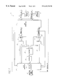
- FIG. 1 is a block diagram of an IDE controller compare circuit capable of receiving and transmitting data from/to a primary drive and receiving and transmitting data from/to a secondary drive in accordance with the invention.
- FIG. 2 is a block diagram of a synchronization circuit for the IDE controller compare circuit of FIG. 1 which synchronizes the transmission of data, the calculation of CRC values and then subsequent storage.
- FIG. 3 is a timing diagram of the synchronization control signals which are propagated through the synchronization circuit of FIG. 2 .
- FIG. 4 is a block diagram of a synchronization circuit for the IDE controller compare circuit of FIG. 1 which synchronizes the operation of transmitting a new dataword to the CRC/checksum circuit, performing the checksum operation and storing the results in the respective accumulation register for each channel.
- FIG. 5 is a timing diagram of the synchronization control signals that are propagated through the synchronization circuit of FIG. 4 .
- Mirrored disk configurations are used throughout the PC industry especially with network server class machines. In network configurations, it is very important to maintain data integrity as well as performance. This invention strives to provide both. This invention will simultaneously calculate a CRC or checksum on the data that is moved from each mirrored disk and then provide a comparison status of two disks. The simultaneous reading of data from each of the mirrored channels and calculation of CRC or checksum values provides increased data throughput over prior IDE controllers which performed these operations for one channel at a time. Additionally, previous IDE controllers did not have the compare circuitry built into them. Instead they relied on software to compare the data between the mirrored disks. Software is inherently slower than a hardware implementation because it must perform extra CPU and memory cycles to compare the data moved from each disk.
- each channel receives a dataword from one of two mirrored disks. A CRC/checksum calculation is then performed on each dataword and the result is stored in respective accumulation registers for each channel of the IDE controller. Upon receiving the next dataword, each channel performs a CRC/checksum calculation by implementing a predetermined CRC algorithm. In one embodiment, each new dataword is combined with the previously calculated CRC value using XOR gates to implement a specific polynomial function in order to produce a new CRC/checksum value.
- this invention is not limited to any specific CRC or checksum algorithm but may include any one of numerous data integrity algorithms which are well-known in the art.
- a dataword is a 16-bit dataword, which is an industry standard. However, datawords having lengths greater than or less than 16-bits may be used in the present invention. As used herein, the term “dataword” refers to any unit of data being a specified number of bits in width, such as, 16-bits or 32-bits.
- the IDE controller 10 includes an IDE interface 11 having a primary IDE channel 13 and a secondary IDE channel 15 .
- a first drive 17 is shown coupled to the primary IDE channel 13 and a second drive 19 is shown connected to the secondary IDE channel 15 .
- Primary data is transmitted on the primary channel 13 to a primary CRC circuit 25 and secondary data is transmitted on the secondary channel 15 to a secondary CRC circuit 27 .
- the primary CRC circuit 25 and the secondary CRC circuit 27 each have an output to an accumulation register 29 , 31 , respectively.
- accumulation registers 29 , 31 store the intermediate values of the CRC/checksum calculations performed on each dataword received by the respective CRC/checksum circuits 25 , 27 .
- the outputs of the accumulation registers 29 and 31 are fed back to their respective CRC circuits 25 , 27 to provide feedback signals that can then be used in performing the CRC/checksum algorithm for the next dataword transferred to the CRC/checksum circuit 25 , 27 .
- the outputs of the accumulation registers 29 , 31 are also communicated to a compare circuit 37 which compares the CRC/checksum values stored in the accumulation registers 29 , 31 and outputs a value of “true” if the comparison indicates an identical match between the values. Otherwise, a “false” value is generated by the compare circuit 37 .
- the output of the compare circuit 37 is then transmitted to a status register 39 which stores the compare value when a synchronizing clock pulse is received.
- the IDE controller 10 also includes a host interface 41 for storing the primary and secondary data 21 , 23 , in a buffer 42 within the host interface 41 .
- the host interface 41 couples a host CPU (not shown) to the IDE controller 10 via a host data and control bus 43 .
- the compare value generated by the compare circuit 37 is accessed by the host CPU via the host interface 41 and the host data and control bus 43 .
- the host CPU will then access all the data stored in the host interface buffer 42 via the host data and control bus 43 and store this data in a main memory of the system, e.g., a hard disk drive.
- the host CPU will then initiate an error correction/analysis program, such as those found in popular network operating systems manufactured by Novell® or Digital Equipment Corp., in order to correct or discard the corrupted data.
- error correction/analysis programs are well known in the art.
- Data may be transmitted between a host CPU and the IDE controller via programmed I/O (PIO) or via direct memory access (DMA).
- PIO programmed I/O
- DMA direct memory access
- the host computer transmits a memory address and a read or write command to the respective drive, for each dataword which is being read from or written to the drive.
- commands include the reading of status and error information, the setting of parameters and the writing of commands. It is called PIO because, in contrast to DMA, every access is individually programmed.
- IDE controller In the DMA mode, apart from the initial request, transfers may take place without intervention by the CPU.
- the CPU transmits “logical block addresses” to a respective drive it desires to access. These “logical block addresses” are then stored in task registers residing within the drive. After the “logical block addresses” are stored in the task registers of the respective disk drives, the CPU will then send a read command to each of the respective disk drives, at which point the IDE controller will initiate a transfer of all the data corresponding to the logical block addresses.
- the IDE controller functions as a bus master ATA compatible (IDE) disk controller that directly moves data between the IDE devices and the main memory of the CPU.
- IDE bus master ATA compatible
- the IDE controller By performing the IDE data transfer as a bus master, the IDE controller off-loads the CPU (no programmed I/O for data transfer) and improves system performance in multitasking environments. This type of transfer mode is advantageous in multi-tasking systems because while one process waits for its I/O access to be completed, the CPU is free to do computations for other processes.
- the allocation or designation of logical block addresses is implemented by a pointer which points to a Physical Region Descriptor Table located in the main memory of the system.
- This table contains some number of physical region descriptors (PRD) which describe areas of memory that are involved in the data transfer.
- PRD physical region descriptors
- the descriptor table is typically aligned on a four byte boundary and the table typically does not cross a 64 k byte boundary in memory.
- PRD physical region descriptors
- the physical memory region to be transferred is described by a PRD.
- Each physical region descriptor entry is typically eight bytes in length. The first four bytes specify the byte address of a physical memory region.
- the next two bytes specify the count of the region in bytes (64 k byte limit per region). A value of zero in these two bytes indicates 64 k bytes. Bit 7 of the last byte indicates the end of the table and the bus master operation terminates when the last PRD has been read. Thus, the data transfer proceeds until all regions described by the PRDs in the table have been transferred.
- DMA transfers involve more work for the processor before and after each transfer, the processor is completely free during the transfer. Also, during the transfer of multiple sectors, an interrupt occurs only at the end of the entire transfer, not after each sector. This is especially advantageous in multitasking systems where the processor can utilize the time it gains through DMA.
- the CPU sets the command register of the IDE controller to a read or write state. If the command register of the IDE controller is set to a read state, for example, the controller will begin transferring the data designated by the logical block addresses to the host interface 41 .
- FIG. 2 shows an embodiment of a master synchronization circuit 12 which is used in the IDE controller of FIG. 1 .
- the first drive 17 (FIG. 1) transmits an interrupt signal, designated as PRI_IRQ, to the IDE interface and the second drive 19 (FIG. 1) transmits an interrupt, SEC_IRQ, to the IDE interface 11 .
- the IDE interface 11 may include a D flip-flop 53 which captures the PRI_IRQ signal and another D flip-flop 57 which captures the SEC_IRQ signal. Since the speed and latency of each drive can vary from access to access, it cannot be determined which drive, primary or secondary, will finish its transfer first and thereafter generate the appropriate interrupt request signal (IRQ).
- D flip-flop 53 the primary drive finishes its data transfer first, for example, it will generate the PRI_IRQ signal, which is usually a logic level high pulse, and transmit this signal to the input of D flip-flop 53 .
- the secondary drive finishes its data transfer first, it will generate the SEC_IRQ signal and transmit it to the input of D flip-flop 57 .
- the outputs of D flip-flop 53 and D flip-flop 57 are “anded” by AND gate 59 .
- D flip-flops are designed to transmit whatever value is present at their inputs upon receiving a rising or falling edge of a clock signal at its clock input.
- the D (delay) flip-flop serves to delay the value of the signal at its input by one clock cycle.
- Digital logic must sometimes deal with input signals that have no fixed temporal relation to a master clock, such as the PRI_IRQ and SEC_IRQ signals of the present invention.
- One natural application of the D flip-flop is as a synchronizer of input signals.
- the output of the AND gate 59 is connected to the D input of the D flip-flop 61 , which has a Q output that serves as a clock pulse to the D flip-flop 39 .
- the D flip-flop 39 is the status register 39 of FIG. 1 . The synchronization of the storage of a compare value into status register 39 , only after the completions of data transfer by both channels, is described in greater detail below with reference to FIG. 3 .
- FIG. 3 shows a timing diagram of the signals propagated through the synchronization circuit 12 of FIG. 2 .
- the primary drive 17 (FIG. 1) generates and outputs an interrupt signal, PRI_IRQ 51 , and transmits this interrupt signal to the D flip-flop 53 of the IDE interface 11 .
- PRI_IRQ becomes active high at time T 0 .
- Q_ 53 goes high at the next rising edge of the clock signal, at time P 0 as seen at 303 .
- the secondary drive when the secondary drive has completed the transfer of a predetermined block or sector of data in response to a read command by the host CPU, the secondary drive will output an interrupt signal, SEC_IRQ, to the IDE interface 11 , at 305 which is time T 1 .
- the signal SEC_IRQ 55 is received by D flip-flop 57 of the synchronization circuit 12 contained within IDE interface 11 .
- the output Q_ 57 of D flip-flop 57 will go high as seen at 307 , on the next rising edge of the master clock signal, at time P 1 .
- Q_ 57 goes high, the two inputs of the AND gate 59 are high.
- the status register 39 stores the compare value at its input, after which this compare value may be accessed by a host CPU. Since the rising edge of Q_ 61 does not occur for at least one clock cycle after the signal SEC_IRQ has gone active high at time T 1 , the master synchronization circuit 12 ensures that the compare value present at the input of the status register, D flip-flop 39 , is not stored and made available to the host CPU until at least one clock cycle after both drives have completed transmitting the specified number of data blocks to the host interface 41 and have generated respective interrupt signals.
- each channel, primary 13 and secondary 15 contains a synchronization circuit 14 for synchronizing the operations of transmitting datawords to their respective CRC circuits, performing CRC/checksum calculations on each dataword, and subsequently clocking the checksum values into the respective accumulation registers, or D flip-flops 29 , 31 (See FIG. 1 ).
- This synchronization is accomplished with control signals, such as PRI_IORD and SEC_IORD, which are generated by the synchronization circuit 14 .
- a primary dataword is transmitted to the inputs of a set of D flip-flops 73 .
- the length of the dataword is 16 bits . Since each of the D flip-flops receives a single bit of the 16 bit primary dataword, there are 16 parallel D flip-flops 73 in the circuit of that embodiment.
- the frequency and number of datawords that are transmitted to the D flip-flops 73 is controlled by a control signal, typically an I/O pulse train, generated by an I/O read circuit 74 .
- the I/O read circuit 74 begins generating a pulse train of specified pulse width and frequency upon receiving a read command signal from the host CPU (not shown). This pulse train is connected to the D input of D flip-flop 75 .
- the complimentary ⁇ overscore (Q) ⁇ output is at a low logic level.
- the ⁇ overscore (Q) ⁇ output of flip-flop 75 functions as the primary I/O read signal, PRI_IORD, which is sent to the primary disk drive (FIG. 1) in order to initiate a read access.
- the PRI_IORD signal is active low such that when its value is at a low logic level, the primary disk drive will access a dataword from a specified memory location and place the dataword on the primary IDE bus 13 (FIG. 1 ). This dataword is then propagated on to the inputs of D flip-flop 73 via the IDE bus 13 .
- This sequence of accessing a dataword and then propagating this dataword to the input of the D flip-flop 73 occurs during the period of time when the PRI_IORD signal is at a low logic level.
- the complimentary output of D flip-flop 75 will go high at the next rising edge of the master clock signal, thus making the PRI_IORD signal high and inactive.
- the primary disk drive is disabled from accessing a dataword and placing it on to the primary IDE bus.
- the complimentary output goes to the inactive high state, it serves as a clocking signal which is connected to the clock inputs of the D flip-flops 73 . Therefore, upon the rising edge of the output of flip-flop 75 , a dataword present at the input of the D flip-flops 73 is clocked into a primary CRC circuit 25 . Thus, in this manner, the frequency and number of datawords which are transmitted to the CRC circuit 25 are controlled.
- synchronization circuit 14 clocks the newly calculated checksum value into the accumulation register 29 one clock cycle after the dataword is clocked into the CRC circuit 25 .
- the new checksum value is clocked into the accumulation register 29 it is thereby stored in the register and fed back to the CRC circuit 25 where it is used to perform a CRC/checksum calculation on the next dataword which is clocked into the CRC circuit 25 .
- the I/O read circuit 74 generates an I/O pulse train of specified pulse width and frequency which controls the frequency and number of datawords transmitted to the input D flip-flops 73 .
- This I/O pulse train is input to the D input of the D flip-flop 75 . Therefore, when the I/O pulse is a logic level high, the complimentary output, ⁇ overscore (Q) ⁇ _ 75 , is a logic level low which serves as the PRI_IORD signal for accessing a dataword and placing the dataword onto the primary IDE bus where it is then propagated to the inputs of the D flip-flop 73 .
- the complimentary output, ⁇ overscore (Q) ⁇ _ 75 is a logic level low which serves as the PRI_IORD signal for accessing a dataword and placing the dataword onto the primary IDE bus where it is then propagated to the inputs of the D flip-flop 73 .
- the complimentary ⁇ overscore (Q) ⁇ output of the D flip-flop 75 is also connected to the input of AND gate 79 .
- the Q output of D flip-flop 75 is connected to the input of the D flip-flop 77 which has a Q output connected to the second input of the AND gate 79 .
- the output of AND gate 79 is connected to the input of a D flip-flop 81 which has a Q output that functions as the clock signal for the accumulation registers 29 .
- a dataword designated as signal D_ 73 is transmitted to the input of the D flip-flop 73 .
- the dataword is a 16-bit dataword and, therefore, there are 16 parallel D flip-flops 73 for receiving each bit of the dataword.
- the signal represented by D_ 73 in FIG. 5 is only one bit of the 16-bit dataword.
- a corresponding data bit signal is simultaneously received at each of the other fifteen D flip-flops 73 .
- this D_ 73 bit value changes from low to high at a time before P 3 .
- this bit value is arbitrarily selected for purposes of illustration.
- the new value received at the input D_ 73 may be a low value as indicated by the dashed lines associated with the signal D_ 73 .
- the dashed lines associated with signals Q_ 73 and Q_ 29 correspond to a low value at the input D_ 73 .
- the accumulation registers 29 / 31 are not clocked by Q_ 81 until at least one clock cycle after the I/O pulse signal from the I/O read circuit 74 has gone low.
- the I/O pulse signal goes low, a dataword has been transmitted by the primary disk drive 17 , via the primary IDE bus 13 , to the input of the D flip-flop 73 .
- the pulse width of the I/O pulse signal generated by the I/O read circuit ensures that this will be the case.
- I/O read circuit 74 may be one of numerous designs for such circuits which are well-known in the art and need not be further discussed here.
- the accumulation registers 29 are clocked by signal Q_ 81 one clock cycle after the ⁇ overscore (Q) ⁇ complimentary output of D flip-flop 75 has clocked the dataword present at the input of D flip-flop 73 into the CRC/checksum circuit 25 . Therefore, each new CRC/checksum value is stored in the accumulation register 29 before or at the same time that the next dataword is clocked into the CRC/checksum circuit 25 , where the new CRC value is used to calculate a new CRC value for the next dataword. In this manner, the synchronization circuit synchronizes the transmission of each dataword with the CRC calculations performed on each dataword.
- each CRC/checksum value is a 16-bit dataword
- the accumulation registers 29 comprise 16 parallel D flip-flops, each used for storing a bit of the 16-bit dataword.
- Each D flip-flop 29 has a clock input which simultaneously receives clock signal Q_ 81 as described above.
- the invention provides an IDE controller which can substantially simultaneously access data from two mirrored disks, in a parallel fashion, substantially simultaneously perform CRC/checksum calculations on data received from each mirrored disk, and compare the CRC/checksum values for each in order to verify data integrity.
- the present invention provides for greater reliability, throughput and faster data access by a computer system.
Abstract
Description
Claims (21)
Priority Applications (1)
| Application Number | Priority Date | Filing Date | Title |
|---|---|---|---|
| US09/251,954 US6434720B1 (en) | 1997-06-23 | 1999-02-17 | Method of checking data integrity for a RAID 1 system |
Applications Claiming Priority (2)
| Application Number | Priority Date | Filing Date | Title |
|---|---|---|---|
| US08/880,251 US5953352A (en) | 1997-06-23 | 1997-06-23 | Method of checking data integrity for a raid 1 system |
| US09/251,954 US6434720B1 (en) | 1997-06-23 | 1999-02-17 | Method of checking data integrity for a RAID 1 system |
Related Parent Applications (1)
| Application Number | Title | Priority Date | Filing Date |
|---|---|---|---|
| US08/880,251 Continuation US5953352A (en) | 1997-06-23 | 1997-06-23 | Method of checking data integrity for a raid 1 system |
Publications (1)
| Publication Number | Publication Date |
|---|---|
| US6434720B1 true US6434720B1 (en) | 2002-08-13 |
Family
ID=25375848
Family Applications (2)
| Application Number | Title | Priority Date | Filing Date |
|---|---|---|---|
| US08/880,251 Expired - Lifetime US5953352A (en) | 1997-06-23 | 1997-06-23 | Method of checking data integrity for a raid 1 system |
| US09/251,954 Expired - Lifetime US6434720B1 (en) | 1997-06-23 | 1999-02-17 | Method of checking data integrity for a RAID 1 system |
Family Applications Before (1)
| Application Number | Title | Priority Date | Filing Date |
|---|---|---|---|
| US08/880,251 Expired - Lifetime US5953352A (en) | 1997-06-23 | 1997-06-23 | Method of checking data integrity for a raid 1 system |
Country Status (1)
| Country | Link |
|---|---|
| US (2) | US5953352A (en) |
Cited By (13)
| Publication number | Priority date | Publication date | Assignee | Title |
|---|---|---|---|---|
| US20010047461A1 (en) * | 1999-02-02 | 2001-11-29 | Storage Technology Corporation | Systems and methods for relocation of compressed data tracks |
| US20030229836A1 (en) * | 2002-02-22 | 2003-12-11 | Seiko Epson Corporation | Integrated circuit |
| US6678861B1 (en) * | 2000-08-21 | 2004-01-13 | Cypress Semiconductor Corp. | FIFO with CRC in a PLD |
| US6678107B1 (en) * | 2001-06-15 | 2004-01-13 | Lsi Logic Corporation | System and method for reading and writing N-way mirrored storage devices |
| US6763398B2 (en) * | 2001-08-29 | 2004-07-13 | International Business Machines Corporation | Modular RAID controller |
| US20040186931A1 (en) * | 2001-11-09 | 2004-09-23 | Gene Maine | Transferring data using direct memory access |
| US20050195903A1 (en) * | 2004-03-04 | 2005-09-08 | Pace Soft Silicon Pvt. Ltd. | Method and apparatus to check for wrongly decoded macroblocks in streaming multimedia applications |
| US20070019649A1 (en) * | 2005-07-20 | 2007-01-25 | Nec Corporation | Data transfer apparatus and data transfer method therefor |
| US20070044002A1 (en) * | 1998-06-11 | 2007-02-22 | Johnson Michael W | Offload system, method, and computer program product for performing cyclical redundancy check (CRC)-related calculations |
| US7249306B2 (en) * | 2004-02-20 | 2007-07-24 | Nvidia Corporation | System and method for generating 128-bit cyclic redundancy check values with 32-bit granularity |
| US20090024907A1 (en) * | 2007-07-17 | 2009-01-22 | Texas Instruments Incorporated | Crc syndrome generation for multiple data input widths |
| US20090187806A1 (en) * | 2004-10-07 | 2009-07-23 | Dell Products L.P. | System and method for error detection in a redundant memory system |
| US9760293B2 (en) | 2013-03-07 | 2017-09-12 | Seagate Technology Llc | Mirrored data storage with improved data reliability |
Families Citing this family (25)
| Publication number | Priority date | Publication date | Assignee | Title |
|---|---|---|---|---|
| US5953352A (en) * | 1997-06-23 | 1999-09-14 | Micron Electronics, Inc. | Method of checking data integrity for a raid 1 system |
| US6170046B1 (en) * | 1997-10-28 | 2001-01-02 | Mmc Networks, Inc. | Accessing a memory system via a data or address bus that provides access to more than one part |
| US6772108B1 (en) * | 1999-09-22 | 2004-08-03 | Netcell Corp. | Raid controller system and method with ATA emulation host interface |
| US6496951B1 (en) * | 1999-12-29 | 2002-12-17 | Emc Corporation | Method for testing signal integrity in a data storage system |
| US6530043B1 (en) | 2000-03-09 | 2003-03-04 | International Business Machines Corporation | Write data error checking in a PCI Bus system |
| TW544578B (en) * | 2001-03-09 | 2003-08-01 | Via Tech Inc | Data transmission device |
| US6934904B2 (en) * | 2001-04-30 | 2005-08-23 | Sun Microsystems, Inc. | Data integrity error handling in a redundant storage array |
| US6886108B2 (en) * | 2001-04-30 | 2005-04-26 | Sun Microsystems, Inc. | Threshold adjustment following forced failure of storage device |
| US6981171B2 (en) * | 2001-06-05 | 2005-12-27 | Sun Microsystems, Inc. | Data storage array employing block verification information to invoke initialization procedures |
| US6928509B2 (en) * | 2002-08-01 | 2005-08-09 | International Business Machines Corporation | Method and apparatus for enhancing reliability and scalability of serial storage devices |
| US6957301B2 (en) * | 2002-09-18 | 2005-10-18 | International Business Machines Corporation | System and method for detecting data integrity problems on a data storage device |
| US7103826B2 (en) * | 2003-07-31 | 2006-09-05 | Hewlett-Packard Development Company, L.P. | Memory system and controller for same |
| US7099994B2 (en) * | 2003-09-29 | 2006-08-29 | Hewlett-Packard Development Company, L.P. | RAID memory system |
| US7360118B1 (en) * | 2003-12-09 | 2008-04-15 | National Semiconductor Corporation | Method and system for verifying data in a shadow memory |
| US7516246B2 (en) * | 2005-10-27 | 2009-04-07 | International Business Machines Corporation | Communications channel method for verifying integrity of untrusted subsystem responses to a request |
| KR100843199B1 (en) * | 2006-08-10 | 2008-07-02 | 삼성전자주식회사 | High speed IDE interface device and method for the same |
| US8024518B1 (en) * | 2007-03-02 | 2011-09-20 | Netapp, Inc. | Optimizing reads for verification of a mirrored file system |
| JP4606455B2 (en) * | 2007-12-20 | 2011-01-05 | 富士通株式会社 | Storage management device, storage management program, and storage system |
| JP5251457B2 (en) * | 2008-11-27 | 2013-07-31 | 富士通株式会社 | Data transmission device |
| US8286027B2 (en) * | 2010-05-25 | 2012-10-09 | Oracle International Corporation | Input/output device including a mechanism for accelerated error handling in multiple processor and multi-function systems |
| US8484400B2 (en) * | 2011-02-01 | 2013-07-09 | Taejin Info Tech Co., Ltd. | Raid-based storage control board |
| US8438324B2 (en) * | 2011-02-01 | 2013-05-07 | Taejin Info Tech Co., Ltd. | RAID-based storage control board having fibre channel interface controller |
| US9436722B1 (en) * | 2013-03-13 | 2016-09-06 | Emc Corporation | Parallel checksumming of data chunks of a shared data object using a log-structured file system |
| DE102013208530A1 (en) * | 2013-05-08 | 2014-11-13 | Robert Bosch Gmbh | memory device |
| US20240039991A1 (en) * | 2022-08-01 | 2024-02-01 | Baker Hughes Holdings Llc | Automated borescope data synchronization |
Citations (26)
| Publication number | Priority date | Publication date | Assignee | Title |
|---|---|---|---|---|
| US4639921A (en) | 1985-01-09 | 1987-01-27 | Sytek, Inc. | Method and an apparatus for early bit collision detection |
| US4979108A (en) | 1985-12-20 | 1990-12-18 | Ag Communication Systems Corporation | Task synchronization arrangement and method for remote duplex processors |
| US5138710A (en) | 1990-04-25 | 1992-08-11 | Unisys Corporation | Apparatus and method for providing recoverability in mass storage data base systems without audit trail mechanisms |
| US5257391A (en) | 1991-08-16 | 1993-10-26 | Ncr Corporation | Disk controller having host interface and bus switches for selecting buffer and drive busses respectively based on configuration control signals |
| US5261058A (en) | 1990-11-09 | 1993-11-09 | Conner Peripherals, Inc. | Multiple microcontroller hard disk drive control architecture |
| US5280487A (en) | 1989-06-16 | 1994-01-18 | Telefonaktiebolaget L M Ericsson | Method and arrangement for detecting and localizing errors or faults in a multi-plane unit incorporated in a digital time switch |
| US5323403A (en) | 1990-08-31 | 1994-06-21 | International Business Machines Corporation | Method and apparatus for maximizing process throughput |
| US5379417A (en) | 1991-11-25 | 1995-01-03 | Tandem Computers Incorporated | System and method for ensuring write data integrity in a redundant array data storage system |
| US5388108A (en) | 1992-10-23 | 1995-02-07 | Ncr Corporation | Delayed initiation of read-modify-write parity operations in a raid level 5 disk array |
| US5412666A (en) | 1990-11-09 | 1995-05-02 | Conner Peripherals, Inc. | Disk drive data path integrity control architecture |
| US5418925A (en) | 1992-10-23 | 1995-05-23 | At&T Global Information Solutions Company | Fast write I/O handling in a disk array using spare drive for buffering |
| US5471640A (en) | 1992-07-06 | 1995-11-28 | Hewlett-Packard | Programmable disk array controller having n counters for n disk drives for stripping data where each counter addresses specific memory location by a count n |
| US5487160A (en) | 1992-12-04 | 1996-01-23 | At&T Global Information Solutions Company | Concurrent image backup for disk storage system |
| US5542065A (en) | 1995-02-10 | 1996-07-30 | Hewlett-Packard Company | Methods for using non-contiguously reserved storage space for data migration in a redundant hierarchic data storage system |
| US5546558A (en) | 1994-06-07 | 1996-08-13 | Hewlett-Packard Company | Memory system with hierarchic disk array and memory map store for persistent storage of virtual mapping information |
| US5548712A (en) | 1995-01-19 | 1996-08-20 | Hewlett-Packard Company | Data storage system and method for managing asynchronous attachment and detachment of storage disks |
| US5553230A (en) | 1995-01-18 | 1996-09-03 | Hewlett-Packard Company | Identifying controller pairs in a dual controller disk array |
| US5592618A (en) | 1994-10-03 | 1997-01-07 | International Business Machines Corporation | Remote copy secondary data copy validation-audit function |
| US5629949A (en) | 1993-09-21 | 1997-05-13 | Cirrus Logic, Inc. | Error correction verification method and apparatus using CRC check remainders |
| US5724368A (en) | 1993-11-04 | 1998-03-03 | Cirrus Logic, Inc. | Cyclical redundancy check method and apparatus |
| US5778206A (en) | 1995-07-19 | 1998-07-07 | Sextant Avionique | Device for interfacing between a redundant-architecture computer and a means of communication |
| US5799022A (en) | 1996-07-01 | 1998-08-25 | Sun Microsystems, Inc. | Faulty module location in a fault tolerant computer system |
| US5953352A (en) * | 1997-06-23 | 1999-09-14 | Micron Electronics, Inc. | Method of checking data integrity for a raid 1 system |
| US6058462A (en) * | 1998-01-23 | 2000-05-02 | International Business Machines Corporation | Method and apparatus for enabling transfer of compressed data record tracks with CRC checking |
| US6062822A (en) * | 1995-07-29 | 2000-05-16 | Alfred Karcher Gmbh & Co. | High-pressure cleaning apparatus |
| US6125469A (en) * | 1994-10-18 | 2000-09-26 | Cirrus Logic, Inc. | Error correction method and apparatus |
-
1997
- 1997-06-23 US US08/880,251 patent/US5953352A/en not_active Expired - Lifetime
-
1999
- 1999-02-17 US US09/251,954 patent/US6434720B1/en not_active Expired - Lifetime
Patent Citations (26)
| Publication number | Priority date | Publication date | Assignee | Title |
|---|---|---|---|---|
| US4639921A (en) | 1985-01-09 | 1987-01-27 | Sytek, Inc. | Method and an apparatus for early bit collision detection |
| US4979108A (en) | 1985-12-20 | 1990-12-18 | Ag Communication Systems Corporation | Task synchronization arrangement and method for remote duplex processors |
| US5280487A (en) | 1989-06-16 | 1994-01-18 | Telefonaktiebolaget L M Ericsson | Method and arrangement for detecting and localizing errors or faults in a multi-plane unit incorporated in a digital time switch |
| US5138710A (en) | 1990-04-25 | 1992-08-11 | Unisys Corporation | Apparatus and method for providing recoverability in mass storage data base systems without audit trail mechanisms |
| US5323403A (en) | 1990-08-31 | 1994-06-21 | International Business Machines Corporation | Method and apparatus for maximizing process throughput |
| US5261058A (en) | 1990-11-09 | 1993-11-09 | Conner Peripherals, Inc. | Multiple microcontroller hard disk drive control architecture |
| US5412666A (en) | 1990-11-09 | 1995-05-02 | Conner Peripherals, Inc. | Disk drive data path integrity control architecture |
| US5257391A (en) | 1991-08-16 | 1993-10-26 | Ncr Corporation | Disk controller having host interface and bus switches for selecting buffer and drive busses respectively based on configuration control signals |
| US5379417A (en) | 1991-11-25 | 1995-01-03 | Tandem Computers Incorporated | System and method for ensuring write data integrity in a redundant array data storage system |
| US5471640A (en) | 1992-07-06 | 1995-11-28 | Hewlett-Packard | Programmable disk array controller having n counters for n disk drives for stripping data where each counter addresses specific memory location by a count n |
| US5388108A (en) | 1992-10-23 | 1995-02-07 | Ncr Corporation | Delayed initiation of read-modify-write parity operations in a raid level 5 disk array |
| US5418925A (en) | 1992-10-23 | 1995-05-23 | At&T Global Information Solutions Company | Fast write I/O handling in a disk array using spare drive for buffering |
| US5487160A (en) | 1992-12-04 | 1996-01-23 | At&T Global Information Solutions Company | Concurrent image backup for disk storage system |
| US5629949A (en) | 1993-09-21 | 1997-05-13 | Cirrus Logic, Inc. | Error correction verification method and apparatus using CRC check remainders |
| US5724368A (en) | 1993-11-04 | 1998-03-03 | Cirrus Logic, Inc. | Cyclical redundancy check method and apparatus |
| US5546558A (en) | 1994-06-07 | 1996-08-13 | Hewlett-Packard Company | Memory system with hierarchic disk array and memory map store for persistent storage of virtual mapping information |
| US5592618A (en) | 1994-10-03 | 1997-01-07 | International Business Machines Corporation | Remote copy secondary data copy validation-audit function |
| US6125469A (en) * | 1994-10-18 | 2000-09-26 | Cirrus Logic, Inc. | Error correction method and apparatus |
| US5553230A (en) | 1995-01-18 | 1996-09-03 | Hewlett-Packard Company | Identifying controller pairs in a dual controller disk array |
| US5548712A (en) | 1995-01-19 | 1996-08-20 | Hewlett-Packard Company | Data storage system and method for managing asynchronous attachment and detachment of storage disks |
| US5542065A (en) | 1995-02-10 | 1996-07-30 | Hewlett-Packard Company | Methods for using non-contiguously reserved storage space for data migration in a redundant hierarchic data storage system |
| US5778206A (en) | 1995-07-19 | 1998-07-07 | Sextant Avionique | Device for interfacing between a redundant-architecture computer and a means of communication |
| US6062822A (en) * | 1995-07-29 | 2000-05-16 | Alfred Karcher Gmbh & Co. | High-pressure cleaning apparatus |
| US5799022A (en) | 1996-07-01 | 1998-08-25 | Sun Microsystems, Inc. | Faulty module location in a fault tolerant computer system |
| US5953352A (en) * | 1997-06-23 | 1999-09-14 | Micron Electronics, Inc. | Method of checking data integrity for a raid 1 system |
| US6058462A (en) * | 1998-01-23 | 2000-05-02 | International Business Machines Corporation | Method and apparatus for enabling transfer of compressed data record tracks with CRC checking |
Non-Patent Citations (3)
| Title |
|---|
| Nebus, James F., "Parallel Data Compression for Fault Tolerance," Computer Design, Apr. 5, 1983, pp. 127-134. |
| Patterson, David, et al., "A Case for redundant Arrays of Inexpensive Disks (RAID)," University of California Report No. UCB/CSD 87/391, Dec. 1987, pp. 109-116. |
| Patterson, David, et al., "Introduction to Redundant Arrays of Inexpensive Disks (RAID)," Compcon '89: 34th IEEE Computer Society International Conference held in San Francisco, Feb. 27, 1989, pp. 112-117. |
Cited By (17)
| Publication number | Priority date | Publication date | Assignee | Title |
|---|---|---|---|---|
| US20070044002A1 (en) * | 1998-06-11 | 2007-02-22 | Johnson Michael W | Offload system, method, and computer program product for performing cyclical redundancy check (CRC)-related calculations |
| US6751714B2 (en) * | 1999-02-02 | 2004-06-15 | Storage Technology Corporation | Systems and methods for relocation of compressed data tracks |
| US20010047461A1 (en) * | 1999-02-02 | 2001-11-29 | Storage Technology Corporation | Systems and methods for relocation of compressed data tracks |
| US6678861B1 (en) * | 2000-08-21 | 2004-01-13 | Cypress Semiconductor Corp. | FIFO with CRC in a PLD |
| US6678107B1 (en) * | 2001-06-15 | 2004-01-13 | Lsi Logic Corporation | System and method for reading and writing N-way mirrored storage devices |
| US6763398B2 (en) * | 2001-08-29 | 2004-07-13 | International Business Machines Corporation | Modular RAID controller |
| US20040186931A1 (en) * | 2001-11-09 | 2004-09-23 | Gene Maine | Transferring data using direct memory access |
| US7380115B2 (en) * | 2001-11-09 | 2008-05-27 | Dot Hill Systems Corp. | Transferring data using direct memory access |
| US20030229836A1 (en) * | 2002-02-22 | 2003-12-11 | Seiko Epson Corporation | Integrated circuit |
| US7249306B2 (en) * | 2004-02-20 | 2007-07-24 | Nvidia Corporation | System and method for generating 128-bit cyclic redundancy check values with 32-bit granularity |
| US20050195903A1 (en) * | 2004-03-04 | 2005-09-08 | Pace Soft Silicon Pvt. Ltd. | Method and apparatus to check for wrongly decoded macroblocks in streaming multimedia applications |
| US20090187806A1 (en) * | 2004-10-07 | 2009-07-23 | Dell Products L.P. | System and method for error detection in a redundant memory system |
| US8341499B2 (en) * | 2004-10-07 | 2012-12-25 | Dell Products L.P. | System and method for error detection in a redundant memory system |
| US20070019649A1 (en) * | 2005-07-20 | 2007-01-25 | Nec Corporation | Data transfer apparatus and data transfer method therefor |
| US8015476B2 (en) * | 2007-07-17 | 2011-09-06 | Texas Instruments Incorporated | CRC syndrome generation for multiple data input widths |
| US20090024907A1 (en) * | 2007-07-17 | 2009-01-22 | Texas Instruments Incorporated | Crc syndrome generation for multiple data input widths |
| US9760293B2 (en) | 2013-03-07 | 2017-09-12 | Seagate Technology Llc | Mirrored data storage with improved data reliability |
Also Published As
| Publication number | Publication date |
|---|---|
| US5953352A (en) | 1999-09-14 |
Similar Documents
| Publication | Publication Date | Title |
|---|---|---|
| US6434720B1 (en) | Method of checking data integrity for a RAID 1 system | |
| US6061822A (en) | System and method for providing a fast and efficient comparison of cyclic redundancy check (CRC/checks sum) values of two mirrored disks | |
| US5987627A (en) | Methods and apparatus for high-speed mass storage access in a computer system | |
| US6018778A (en) | Disk array controller for reading/writing striped data using a single address counter for synchronously transferring data between data ports and buffer memory | |
| US5890207A (en) | High performance integrated cached storage device | |
| US6161165A (en) | High performance data path with XOR on the fly | |
| US5884055A (en) | Method and apparatus including a shared resource and multiple processors running a common control program accessing the shared resource | |
| US5890219A (en) | Redundant writing of data to cached storage system | |
| US6151641A (en) | DMA controller of a RAID storage controller with integrated XOR parity computation capability adapted to compute parity in parallel with the transfer of data segments | |
| US7574541B2 (en) | FIFO sub-system with in-line correction | |
| US5255374A (en) | Bus interface logic for computer system having dual bus architecture | |
| CA1325286C (en) | Method and apparatus for interfacing a system control unit for a multi-processor system with input/output units | |
| US6289471B1 (en) | Storage device array architecture with solid-state redundancy unit | |
| US5687393A (en) | System for controlling responses to requests over a data bus between a plurality of master controllers and a slave storage controller by inserting control characters | |
| WO1996018141A1 (en) | Computer system | |
| US6678768B1 (en) | Method and apparatus for configuring redundant array of independent disks (RAID) | |
| EP0825534B1 (en) | Method and apparatus for parity block generation | |
| US6370616B1 (en) | Memory interface controller for datum raid operations with a datum multiplier | |
| US5838892A (en) | Method and apparatus for calculating an error detecting code block in a disk drive controller | |
| US5062044A (en) | Temporary bus master for use in a digital system having asynchronously communicating sub-systems | |
| US20040128602A1 (en) | Direct memory access with error correction | |
| EP0492072A1 (en) | Data transfer bus system and method serving multiple parallel asynchronous units | |
| WO1993013475A1 (en) | Method for performing disk array operations using a nonuniform stripe size mapping scheme | |
| US5875458A (en) | Disk storage device | |
| JPS6381660A (en) | Magnetic memory controller |
Legal Events
| Date | Code | Title | Description |
|---|---|---|---|
| AS | Assignment |
Owner name: MEI CALIFORNIA, INC., CALIFORNIA Free format text: ASSIGNMENT OF ASSIGNORS INTEREST;ASSIGNOR:MICRON ELECTRONICS, INC.;REEL/FRAME:011658/0956 Effective date: 20010322 |
|
| AS | Assignment |
Owner name: MICRON TECHNOLOGY, INC., IDAHO Free format text: ASSIGNMENT OF ASSIGNORS INTEREST;ASSIGNOR:MEI CALIFORNIA INC;REEL/FRAME:012232/0436 Effective date: 20010322 |
|
| STCF | Information on status: patent grant |
Free format text: PATENTED CASE |
|
| FEPP | Fee payment procedure |
Free format text: PAYOR NUMBER ASSIGNED (ORIGINAL EVENT CODE: ASPN); ENTITY STATUS OF PATENT OWNER: LARGE ENTITY |
|
| FPAY | Fee payment |
Year of fee payment: 4 |
|
| FPAY | Fee payment |
Year of fee payment: 8 |
|
| FPAY | Fee payment |
Year of fee payment: 12 |
|
| AS | Assignment |
Owner name: U.S. BANK NATIONAL ASSOCIATION, AS COLLATERAL AGENT, CALIFORNIA Free format text: SECURITY INTEREST;ASSIGNOR:MICRON TECHNOLOGY, INC.;REEL/FRAME:038669/0001 Effective date: 20160426 Owner name: U.S. BANK NATIONAL ASSOCIATION, AS COLLATERAL AGEN Free format text: SECURITY INTEREST;ASSIGNOR:MICRON TECHNOLOGY, INC.;REEL/FRAME:038669/0001 Effective date: 20160426 |
|
| AS | Assignment |
Owner name: MORGAN STANLEY SENIOR FUNDING, INC., AS COLLATERAL AGENT, MARYLAND Free format text: PATENT SECURITY AGREEMENT;ASSIGNOR:MICRON TECHNOLOGY, INC.;REEL/FRAME:038954/0001 Effective date: 20160426 Owner name: MORGAN STANLEY SENIOR FUNDING, INC., AS COLLATERAL Free format text: PATENT SECURITY AGREEMENT;ASSIGNOR:MICRON TECHNOLOGY, INC.;REEL/FRAME:038954/0001 Effective date: 20160426 |
|
| AS | Assignment |
Owner name: U.S. BANK NATIONAL ASSOCIATION, AS COLLATERAL AGENT, CALIFORNIA Free format text: CORRECTIVE ASSIGNMENT TO CORRECT THE REPLACE ERRONEOUSLY FILED PATENT #7358718 WITH THE CORRECT PATENT #7358178 PREVIOUSLY RECORDED ON REEL 038669 FRAME 0001. ASSIGNOR(S) HEREBY CONFIRMS THE SECURITY INTEREST;ASSIGNOR:MICRON TECHNOLOGY, INC.;REEL/FRAME:043079/0001 Effective date: 20160426 Owner name: U.S. BANK NATIONAL ASSOCIATION, AS COLLATERAL AGEN Free format text: CORRECTIVE ASSIGNMENT TO CORRECT THE REPLACE ERRONEOUSLY FILED PATENT #7358718 WITH THE CORRECT PATENT #7358178 PREVIOUSLY RECORDED ON REEL 038669 FRAME 0001. ASSIGNOR(S) HEREBY CONFIRMS THE SECURITY INTEREST;ASSIGNOR:MICRON TECHNOLOGY, INC.;REEL/FRAME:043079/0001 Effective date: 20160426 |
|
| AS | Assignment |
Owner name: MICRON TECHNOLOGY, INC., IDAHO Free format text: RELEASE BY SECURED PARTY;ASSIGNOR:U.S. BANK NATIONAL ASSOCIATION, AS COLLATERAL AGENT;REEL/FRAME:047243/0001 Effective date: 20180629 |
|
| AS | Assignment |
Owner name: MICRON TECHNOLOGY, INC., IDAHO Free format text: RELEASE BY SECURED PARTY;ASSIGNOR:MORGAN STANLEY SENIOR FUNDING, INC., AS COLLATERAL AGENT;REEL/FRAME:050937/0001 Effective date: 20190731 |