US6285754B1 - Odd-order low-pass pots device microfilter - Google Patents
Odd-order low-pass pots device microfilter Download PDFInfo
- Publication number
- US6285754B1 US6285754B1 US09/544,731 US54473100A US6285754B1 US 6285754 B1 US6285754 B1 US 6285754B1 US 54473100 A US54473100 A US 54473100A US 6285754 B1 US6285754 B1 US 6285754B1
- Authority
- US
- United States
- Prior art keywords
- filter
- inductors
- telephone wiring
- wiring network
- khz
- Prior art date
- Legal status (The legal status is an assumption and is not a legal conclusion. Google has not performed a legal analysis and makes no representation as to the accuracy of the status listed.)
- Expired - Lifetime
Links
- 239000003990 capacitor Substances 0.000 claims abstract description 42
- 230000002441 reversible effect Effects 0.000 claims abstract description 23
- 238000004804 winding Methods 0.000 claims description 13
- 230000001052 transient effect Effects 0.000 claims description 9
- 239000011324 bead Substances 0.000 claims description 8
- 231100001261 hazardous Toxicity 0.000 claims description 5
- 229910000859 α-Fe Inorganic materials 0.000 claims description 5
- 238000003780 insertion Methods 0.000 claims description 3
- 230000037431 insertion Effects 0.000 claims description 3
- 230000006855 networking Effects 0.000 abstract description 17
- 230000004044 response Effects 0.000 abstract description 17
- 101150012579 ADSL gene Proteins 0.000 abstract 1
- 102100020775 Adenylosuccinate lyase Human genes 0.000 abstract 1
- 108700040193 Adenylosuccinate lyases Proteins 0.000 abstract 1
- 230000008901 benefit Effects 0.000 description 9
- 239000011162 core material Substances 0.000 description 6
- 230000002452 interceptive effect Effects 0.000 description 6
- 230000005540 biological transmission Effects 0.000 description 4
- 239000000969 carrier Substances 0.000 description 4
- 238000000034 method Methods 0.000 description 4
- 238000010586 diagram Methods 0.000 description 3
- 238000009434 installation Methods 0.000 description 3
- 230000006735 deficit Effects 0.000 description 2
- 238000001914 filtration Methods 0.000 description 2
- 238000004519 manufacturing process Methods 0.000 description 2
- 230000001105 regulatory effect Effects 0.000 description 2
- 238000001228 spectrum Methods 0.000 description 2
- 230000001629 suppression Effects 0.000 description 2
- 230000032258 transport Effects 0.000 description 2
- RYGMFSIKBFXOCR-UHFFFAOYSA-N Copper Chemical compound [Cu] RYGMFSIKBFXOCR-UHFFFAOYSA-N 0.000 description 1
- 230000002411 adverse Effects 0.000 description 1
- 230000002238 attenuated effect Effects 0.000 description 1
- 230000015556 catabolic process Effects 0.000 description 1
- 230000008859 change Effects 0.000 description 1
- 229910052802 copper Inorganic materials 0.000 description 1
- 239000010949 copper Substances 0.000 description 1
- 238000006731 degradation reaction Methods 0.000 description 1
- 230000000694 effects Effects 0.000 description 1
- 238000005516 engineering process Methods 0.000 description 1
- 238000012986 modification Methods 0.000 description 1
- 230000004048 modification Effects 0.000 description 1
Images


Classifications
-
- H—ELECTRICITY
- H04—ELECTRIC COMMUNICATION TECHNIQUE
- H04M—TELEPHONIC COMMUNICATION
- H04M11/00—Telephonic communication systems specially adapted for combination with other electrical systems
- H04M11/06—Simultaneous speech and data transmission, e.g. telegraphic transmission over the same conductors
- H04M11/062—Simultaneous speech and data transmission, e.g. telegraphic transmission over the same conductors using different frequency bands for speech and other data
-
- H—ELECTRICITY
- H04—ELECTRIC COMMUNICATION TECHNIQUE
- H04L—TRANSMISSION OF DIGITAL INFORMATION, e.g. TELEGRAPHIC COMMUNICATION
- H04L25/00—Baseband systems
- H04L25/02—Details ; arrangements for supplying electrical power along data transmission lines
- H04L25/08—Modifications for reducing interference; Modifications for reducing effects due to line faults ; Receiver end arrangements for detecting or overcoming line faults
- H04L25/085—Arrangements for reducing interference in line transmission systems, e.g. by differential transmission
-
- H—ELECTRICITY
- H04—ELECTRIC COMMUNICATION TECHNIQUE
- H04M—TELEPHONIC COMMUNICATION
- H04M1/00—Substation equipment, e.g. for use by subscribers
- H04M1/738—Interface circuits for coupling substations to external telephone lines
Definitions
- This invention relates generally to low-pass filters and, more particularly, to a reversible, odd-order low-pass microfilter for separating DSL and home networking signals from voice-band signals existing on the same pair of copper wires.
- DSL Digital Subscriber Line
- home networking signals or both present on a home telephone wiring network simultaneously with voice-band signals.
- Voice-band signals are commonly referred to as POTS (Plain Old Telephone Service) signals.
- Voice-band appliances may include, for example, telephone sets, facsimile machines, 56K modems, and the like. Indeed, energy from the DSL or home networking signal carriers may cause nonlinear behavior of the voice-band appliances to create noise into the POTS connection. Further, preventing DSL and home networking signals from reaching voice-band appliances protects the DSL and home networking transports from high-frequency inter-modulation products of the voice-band appliances.
- Voice-band appliances typically undergo impedance changes during operation. For example, state changes in a POTS device such as on/off hook, dialing, and ringing tend to affect the impedance of the POTS device. This change in impedance, unless isolated from the DSL modem, may limit the throughput of the DSL or home networking devices and may require dynamic bit reloading in modulation and line retraining, and could result in loss of modem connection.
- a second-order low-pass Butterworth filter is disposed between the home telephone wiring network and an associated POTS device to prevent DSL signals, such as ADSL signals, on the home telephone wiring network from entering the POTS device and to prevent transient noise from POTS devices from interfering with the proper operation of a DSL modem coupled to the home network and vice versa.
- the filter topology of the second-order Butterworth microfilter is inherently asymmetrical and generally includes one coupled inductor (or two uncoupled inductors) and one capacitor. This design is unilateral and non-reversible in that it requires, for proper operation, that the microfilter be oriented between the POTS device and the home telephone wiring network such that the coupled inductor is disposed between the home telephone wiring network and the capacitor.
- a typical second-order Butterworth microfilter may be designed with an insertion loss of about 0.3 dB loss throughout the pass band, which includes the POTS band (about 0-4 kHz) and has a cutoff frequency of about 8 kHz.
- this cutoff frequency it is highly desirable for this cutoff frequency to be above the POTS signal band and well below the ADSL transmission band (i.e. below about 25 kHz). Given the 8 kHz cutoff frequency, the total attenuation achieved at 25 kHz (the beginning of the DSL band) is, at a maximum, only about 19 dB.
- This amount of attenuation is generally insufficient in that it allows a significant amount of DSL transmit signal leakage through the filter, and could cause interference with the associated POTS device, particularly if the associated POTS device is a data device, such as a facsimile machine or a data modem.
- a significant factor in determining the cost of producing a microfilter is the number of components that make up the microfilter. In general, the higher the number of components that make up the microfilter, the higher the cost will be to produce the microfilter. Consequently, it is desirable to keep the component count of a given microfilter design low to keep the production cost low.
- HPNA Home Phoneline Network Alliance
- the present invention overcomes or substantially alleviates prior problems associated with systems and methods for separating or isolating voice-band appliances from DSL and HPNA devices.
- the present invention provides a reversible odd-order low-pass filter that may be disposed between a POTS device and a home telephone wiring network to isolate the POTS device from certain higher frequency signals, such as DSL band signals, that may be present on the home telephone wiring network.
- the filter also prevents POTS device impedance changes within the DSL band from appearing on the home telephone wiring network.
- the filter topology is substantially symmetric in that the topology features reversible plug-in capability so that either end of the filter may be coupled to the home telephone wiring network without interfering with the filtering function of the filter and without shorting, or shunting, the higher frequency signals, such as ADSL signals, on the home telephone wiring network. Further, the filter presents a relatively low insertion loss so that the filter does not cause significant attenuation of the POTS signal as the POTS signal passes through the filter, thus not impairing the operation of the associated POTS device.
- the low pass filter is a passive odd-order low-pass reversible microfilter that includes a capacitor disposed between pairs of inductors for disposition between the telephone wiring network and an associated POTS device to high frequency signals from reaching the POTS device and for isolating the POTS device impedance changes from the network.
- the inductors may be either coupled or uncoupled inductors.
- the microfilter is reversible in that either end of the microfilter may be disposed adjacent to the to the telephone network without shorting high frequency signals, such as ADSL signals, across the capacitor due to the presence of a pair of inductors on both sides of the capacitors.
- the low-pass filter is a passive third-order low-pass microfilter design scheme based on a 600 ohm balanced network and includes a pair of coupled inductors separated by a capacitor.
- each of the coupled inductors has combined interwinding capacitance greater than about 100 pF. Due to the intentionally-introduced interwinding capacitance of the coupled inductors, the frequency response of the low-pass filter closely resembles that of a higher order Chebyshev II function, also known in the art as an “inverse Chebyshev” function
- This filter function generally has a flatter magnitude response in the pass band than conventional Chebyshev filters and much steeper attenuation beyond the cutoff frequency than the conventional Butterworth filter described above.
- the filter presents more than about 35 dB of attenuation beginning at 25 kHz with a 3 dB cutoff frequency point at about 6 kHz, which offers sufficient signal rejection to prevent DSL signals from reaching the associated POTS band device and potentially causing performance degradation.
- This odd-order design is advantageous in that it effectively and inexpensively isolates high frequency signals, such as DSL signals, on a home telephone wiring network from reaching POTS devices, as well as preventing the impedance changes of the POTS devices from interfering with the DSL or home networking service.
- the odd-order filter does not employ a capacitor disposed outside of the coupled or uncoupled inductors, the filter is reversible in that either end of the filter may be coupled to the home telephone wiring network without shorting, or shunting, the high frequency signals across the capacitor or otherwise impairing the filter characteristic of the filter.
- the filter will still generate the same frequency response and function satisfactorily without shorting the higher frequency signals on the home telephone wiring network.
- the present design provides a microfilter having a single resonant frequency point disposed above the POTS frequency band (i.e. above about 4 kHz) and well below the DSL band (i.e. below about 25 kHz) to avoid introducing unexpected impedance impairments to both POTS and ADSL operations. Additionally, the microfilter provides a relatively high impedance across the DSL frequency band beginning at about 25 kHz for both on-hook and off-hook conditions to block impedance changes caused by an associated POTS device. Moreover, to avoid high signal loss across the DSL band, the microfilter advantageously has an input impedance of at least 400 ohms.
- FIG. 1 is a block diagram illustrating a splittered DSL service network
- FIG. 2 is a block diagram of the splitter of FIG. 1;
- FIG. 3 is a block diagram illustrating a splitterless DSL service network
- FIG. 4A illustrates details of one embodiment of one of the filters of FIGS. 1 and 3, which uses coupled inductors;
- FIG. 4B illustrates details of a circuit electrically equivalent to the filter of FIG. 4A, which uses coupled inductors;
- FIG. 4C illustrates details of another embodiment of one of the filters of FIGS. 1 and 3, which uses uncoupled or discrete inductors;
- FIG. 5 illustrates the filter of FIG. 4A in a reversed installation configuration
- FIG. 6 illustrates the frequency response of the filter of FIG. 4A
- FIG. 7 illustrates the off-hook impedance response of the filter of FIG. 4A.
- FIG. 8 illustrates the on-hook impedance response of the filter of FIG. 4 B.
- FIG. 1 illustrates a DSL, such as ADSL, service network 100 that includes a central office 102 including a Digital Subscriber Line Access Multiplexer (D)SLAM) 103 and a home 104 coupled by a loop 106 .
- the central office 102 includes a DSL modem unit 110 and a loop interface 112 .
- the loop interface 112 includes a high pass filter 114 and a low pass filter 116 to split high frequency DSL components of the loop signal and the lower frequency POTS (Plain Old Telephone Service) components of the loop signal.
- the high pass filter 114 passes signals in the DSL frequency range to the broadband network 120 via the DSL modem 110 .
- the low pass filter 116 passes the lower frequency POTS signals to the narrow band network 122 over a PSTN (Public Switched Telephone Network) line.
- PSTN Public Switched Telephone Network
- the home 104 is shown as including a splitter 130 , a DSL modem 132 , a computer 134 , a home telephone wiring network 136 , and POTS devices, such as telephone 138 and facsimile machine 139 .
- Lines 148 couple the telephone 138 , the facsimile machine 139 , as well as other POTS devices (e.g. 56 k modems, etc.) (not shown), to the home telephone wiring network 136 .
- personal computers 141 and 143 are illustrated as being coupled to the network 136 .
- the computer 141 is shown as having an external HPNA (Home Phoneline Network Alliance) standard network interface card 145 .
- the computer 143 has an internal HPNA card (not shown) so that the computers 141 and 143 may communicate using high-frequency home networking (HPNA standard) signals over the network 136 .
- HPNA Home Phoneline Network Alliance
- the DSL modem 132 is illustrated as being disposed outside of the computer 134 , those skilled in the art will appreciate that the DSL modem 132 could also be positioned inside the computer 134 .
- the splitter 130 splits the incoming signal, which may include DSL signals, POTS signals, or both into high (DSL) and low (POTS) frequency components. As discussed in more detail below with reference to FIG. 2, the splitter 130 routes the high frequency component along line 140 to the DSL modem 132 , which is coupled to a network device, such as a computer 134 , by a line 142 . Likewise, the splitter 130 routes the low frequency, or POTS, component of the incoming signal to the home telephone wiring network 136 along line 144 .
- the telephone 138 , the facsimile machine 139 , as well as other POTS devices (e.g. 56 k modems, etc.) (not shown), are coupled to the home telephone wiring network 136 by lines 148 .
- a low-pass filter 150 is shown as being disposed between each POTS device and the home telephone wiring network 136 .
- the low-pass filters 150 can be used, but may not be required, to prevent the home networking high frequency energy on the home telephone wiring network 136 from reaching the POTS voice-band appliances, such as the telephone 138 and the facsimile machine 139 .
- Home networking, or HPNA standard, signals reside above 2 MHz and usually reside in the band ranging from about 5 MHz to about 10 MHz.
- the filters 150 substantially reduce, or eliminate, the non-linear behavior of the voice-band appliances from creating noise onto the home telephone wiring network 136 and protects home networking transports from high-frequency inter-modulation products from the voice-band appliances.
- ADSL Digital Subscriber Line
- FIG. 2 illustrates details of the splitter 130 of FIG. 1 .
- the splitter 130 includes a high pass filter 202 and a low pass filter 204 coupled to the loop 106 via lines 206 and 208 respectively.
- the high pass filter 202 permits higher frequency signals, such as DSL signals, to pass from the loop 106 to the DSL modem 132 (FIG. 1) while preventing the lower frequency POTS signals from entering onto the line 140 and potentially interfering with the operation of the DSL modem 132 .
- the low pass filter 204 permits the lower frequency POTS signals to pass onto the home telephone wiring network 136 while preventing higher frequency signals, such as DSL signals, from entering onto the home telephone wiring network 136 .
- the splitter 130 also separates or isolates
- FIG. 3 illustrates a splitterless DSL network 300 , such as that which might be used to support DSL service using the International Telecommunications Union (ITU) G.992.2 (G.lite) or G.992.1 (G.dmt) standards, or to support T1.413. Issue 2 full-rate ADSL.
- the network 300 differs from that illustrated in FIG. 1 in that it does not include the splitter 130 disposed between the loop 106 and the home telephone wiring network 136 or the DSL modem 132 .
- the loop 106 is directly coupled to the home telephone wiring network 136 via the line 144 and, therefore, DSL, home networking, and POTS (or voice-band) signals pass simultaneously over the home telephone wiring network 136 .
- the network 300 includes low pass filters 150 disposed between the home telephone wiring network 136 and the voice-band appliances 138 and 139 .
- the low-pass filters 150 generally prevent the higher frequency signals (signals above about 25 kHz) from interfering with operation of the associated voice-band or POTS devices 138 and 139 and separate POTS device impedance changes from the DSL and HPNA signal carriers.
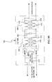
- FIG. 4A illustrates the topology of one embodiment of the filter 150 shown in FIGS. 1 and 3.
- the filter 150 of FIG. 4A is a reversible three-pole odd-order low pass filter and includes first and second coupled inductors, or transformers, 402 and 404 with a capacitor 406 therebetween.
- the filter 150 is shown as having a pair of ferrite beads 408 and a hazardous transient voltage protection circuit 410 .
- the ferrite beads 408 and the hazardous transient voltage protection circuit 410 are optional components and may not be required in all applications. Rather, the beads 408 and the voltage protection circuit 410 may be used for compliance with applicable regulatory requirements.
- the hazardous transient voltage protection circuit 410 comprises a sidactor transient voltage suppressor.
- the filter 150 is further illustrated as being disposed between the home telephone wiring network 136 and a POTS device, such as the telephone 138 (FIG. 1) with the coupled inductor 404 closest to or adjacent the home telephone wiring network 136 .
- a significant advantage of the design of FIG. 4 is that the capacitor 406 is disposed between the two coupled inductors 402 and 404 so that regardless of which end of the filter 150 is coupled to the home telephone wiring network 136 , the capacitor 206 will not short, or shunt, a high frequency signal, such as a DSL signal, on the home telephone wiring network 136 .
- This advantage makes the filter 150 reversible in that either end of the filter 150 may be coupled to the home telephone wiring network 136 without shorting high frequency signals across the capacitor or otherwise impairing transmission of high frequency signals.
- the capacitor 406 advantageously has a capacitance in the range of about 0.022-0.068 microfarads (22-68 nanofarads). For example, pursuant to one embodiment, the capacitor 406 has a capacitance of about 47 nanofarads.
- the first and second coupled inductors 402 and 404 are shown as being configured identical to one another.
- the first coupled inductor 402 includes a pair of windings 412 wrapped about a core 414 .
- each of the windings 412 has an inductance of about 3 mH-7.5 mH ⁇ 10% (about 2.7-8.3 mH) and the core 214 comprises a conventional EP 13, EP10, EP 7 coupled inductor core, although those skilled in the art will appreciate that other coupled inductor core materials could also be employed.
- This coupled inductor configuration yields a relatively high inductance as it includes both the self inductance of each winding together with the mutual inductance of the coupled inductor when AC current flowing through the coupled inductor windings 412 and thereby produces better high frequency attenuation. Further, the interwinding capacitance of the coupled inductors 402 and 404 enhances the filter characteristic of the filter 150 by contributing to a steeper frequency roll off as shown in FIG. 6 .
- each of the coupled inductors 402 and 404 advantageously comprises an interwinding capacitance over about 100 pF in the frequency range of about 10 kHz-100 kHz.
- each of the coupled inductors 402 and 404 comprises an interwinding capacitance in the range of about 1,000-2,000 pF in the frequency range of about 10 kHz-100 kHz.
- Conventional microfilter design generally dictates use of coupled inductors that have relatively low interwinding capacitances so as to have a relatively linear impedance characteristic and to prevent the coupled inductor from behaving like a capacitor. It has, however, been determined that, contrary to conventional microfilter design, there are significant advantages associated with employing coupled inductors having significant interwinding capacitances in DSL microfilters.
- One advantage of employing coupled inductors having interwinding capacitances above about 100 pF is that having a significant interwinding capacitance for each coupled inductor makes the filter 150 behave like a higher-order filter without the cost associated with adding additional filter components.
- this design creates a steeper frequency roll off right after the cutoff frequency point than would be possible with a filter having coupled inductors without significant interwinding capacitances. Since this steeper frequency roll off is achieved without raising the component count of the filter the cost of production is not increased. Too high of an interwinding capacitance, however, may adversely affect the high frequency response of the filter 150 , such as the response above about 2 MHz.
- the amount of interwinding capacitance may need to be balanced or controlled for possible high frequency response requirements.
- the filter 150 maintains its third-order filter impedance characteristics.
- One important third-order filter impedance characteristic is that the impedance characteristic has only one resonant point. Higher order filters typically have multiple resonant points, or low impedance points, which create additional design complexities in preventing these points from residing in or too close to either the POTS or DSL bands.
- the filter 150 behaves like a higher order filter in its frequency characteristic, the filter 150 maintains a single resonant point that safely resides between the POTS and DSL frequency bands.
- Coupled inductors having interwinding capacitances above about 100 pF, and preferably between about 1,000 and 2,000 pF relate to cost. Indeed, as those skilled in the art will appreciate, coupled inductors having little or no interwinding capacitance are typically more expensive than coupled inductors that have an interwinding capacitance greater than about 100 pF. Hence, in addition to the technical advantages of using coupled inductors that have an interwinding capacitance greater than about 100 pF, cost savings in purchasing the coupled inductors may also be effected.
- the ferrite beads 408 reduce high frequency, common mode noise as well as provide EMI suppression.
- the hazardous transient voltage protection circuit 410 is conventional and is used to protect the associated POTS device from being damaged by transient voltages, such as those that might be produced by a lightning strike, for example.
- the beads 408 and the voltage protection circuit 410 are optional components and are not critical to the filtering functions of the filter 150 . Rather, the beads 408 and the voltage protection circuit 410 may be included for regulatory purposes.
- FIG. 4B shows an equivalent circuit 450 that is the electrical equivalent to the filter 150 shown in FIG. 4 A and described above to illustrate the interwinding capacitance of the coupled inductors 402 and 404 (FIG. 4 A).
- the electrical circuit 450 includes coupled inductors 452 and 454 .
- Each coupled inductor 452 and 454 comprises a pair of windings, or inductors, 462 that are wrapped about the inductor core 414 with each winding 462 having an inductance of about 3 mH-7 mH ⁇ 10% and negligible, or no, interwinding capacitance.
- a capacitor 461 is positioned in parallel with each of the windings 462 to model the interwinding capacitance of the coupled inductors 452 and 454 .
- Each capacitor 461 has a capacitance of more than about 100 pF, and preferably a capacitance of about 1,000-2,000 pF for the application of suppression of ADSL noise getting into the associated POTS device.
- the equivalent circuit 450 also includes the capacitor 406 , the beads 408 , and the voltage protection circuit 410 described above with reference to FIG. 4 A.
- the circuit 450 is electrically equivalent to the filter 150 in that the circuit 450 has an identical, or substantially identical, frequency response and impedance characteristic as the filter 150 .
- the equivalent circuit 450 has several additional components, namely the four capacitors 461 , thereby requiring a substantially higher component count than the filter 150 .
- FIG. 4C illustrates another embodiment of the filter 150 wherein the inductor pairs comprise uncoupled inductors 470 , 472 , 474 , and 476 .
- the uncoupled inductors 470 - 476 are configured identically to each other and comprise a winding 480 and a ferrite drum-type core 482 .
- each of the inductors 470 - 476 has an inductance in the range of about 5-15 mH.
- the capacitor 406 preferably has a capacitance of about 0.047 microfarads, but may have a capacitance in the range of 0.022-0.068 microfarads.
- the FIG. 4C embodiment is symmetric and, therefore, reversible.
- the filter 150 of FIG. 4C may be oriented relative to the telephone network 136 as illustrated in FIG. 4C with the inductors 470 and 472 being adjacent to the telephone network 136 or in a reversed orientation (not shown) with the inductors 474 and 476 being adjacent to the telephone network 136 .
- the filter 150 may be disposed in either orientation between the associated POTS device and the telephone network 136 without shorting high frequency signals, such as ADSL signals, on the network 136 across the capacitor 406 .
- a pair of inductors separates the telephone network 136 from the capacitor 406 to prevent high frequency signals, such as ADSL signals, on the network 136 from shorting, or being shunted, across the capacitor 406 .
- FIG. 5 illustrates the reversible nature of the filter 150 of FIG. 4 A.
- the filter 150 of FIG. 4C is similarly reversible. That is, FIG. 5 shows the filter 150 of FIG. 4A coupled to the network 136 (FIG. 1) in a manner opposite that shown in FIG. 4 A. As illustrated in FIG. 5, the filter 150 is disposed between a POTS device, such as the telephone 138 (FIG. 1) and the home telephone wiring network 136 with the home telephone wiring network 136 being coupled to the filter adjacent to the coupled inductor 402 .
- the capacitor 406 is separated from the home telephone wiring network 136 by a coupled inductor.
- the capacitor 406 is separated from the home telephone wiring network 136 by the coupled inductor, or transformer, 404 whereas in FIG. 5, the capacitor 406 is separated from the home telephone wiring network 136 by the coupled inductor 402 .
- FIG. 6 illustrates the frequency response of the filter 150 described above in FIG. 4 A.
- FIG. 6 depicts the filter frequency response based on an approximately 600 ohm balanced impedance.
- the frequency response permits the filter 150 to effectively function as a low-pass filter, permitting passage of signals in the voice band (about 20 Hz-4 kHz), but preventing higher frequency signals, such as those above about 25 kHz from passing therethrough.
- the filter 150 provides negligible, if any, attenuation of voice-band signals below about 4 kHz. For signals above 25 kHz, however, the filter 150 provides over 30 dB of signal attenuation. As an example, for DSL signals in the 100 kHz range, the attenuation is about 56 dB. Another example shows that a 1 MHz signal would be attenuated by about 60 dB. Yet another example shows about 37 dB of attenuation for a 25 kHz signal.
- FIGS. 7 and 8 respectively illustrate off-hook and on-hook impedance characteristics of the filter 150 of FIG. 4A in an embodiment where the capacitor 406 has a capacitance of about 0.047 microfarads.
- the filter 150 provides a relatively high off-hook impedance (above about 400 ohms) in the DSL band to prevent impedance loading and high signal loss across the DSL band.
- the filter 150 will preferably present an impedance greater than about 400 ohms throughout the DSL band for both on-hook and off-hook conditions.
- the filter 150 maintains third order impedance characteristics.
- One impedance characteristic of the filter 150 is that the filter 150 has a single resonant frequency, or resonant point, that resides above the POTS band and below the DSL band.
- a resonant frequency is generally a frequency at which a filter's inductor and capacitor have approximately equal and opposite reactance, which may lead to a low input impedance dip.
- the resonant frequency is shown as residing in the frequency range 4-6 kHz. When this resonant point resides inside the POTS band, serious impedance impairments and a non-flat frequency response in both on-hook and off-hook states could result. Consequently, it is desirable to not have the resonant frequency reside within either the POTS or the DSL bands.
- the filter 150 is advantageous in that, due, at least in part, to the intentionally introduced interwinding capacitance of the coupled inductors 402 and 404 , the filter 150 impedance characteristic has a single resonant point despite having a filter characteristic that resembles that of a higher order filter.
Abstract
Description
Claims (10)
Priority Applications (2)
| Application Number | Priority Date | Filing Date | Title |
|---|---|---|---|
| US09/544,731 US6285754B1 (en) | 2000-04-06 | 2000-04-06 | Odd-order low-pass pots device microfilter |
| US09/943,825 US6694016B1 (en) | 2000-04-06 | 2001-08-30 | Odd-order low-pass POTS device microfilter |
Applications Claiming Priority (1)
| Application Number | Priority Date | Filing Date | Title |
|---|---|---|---|
| US09/544,731 US6285754B1 (en) | 2000-04-06 | 2000-04-06 | Odd-order low-pass pots device microfilter |
Related Child Applications (1)
| Application Number | Title | Priority Date | Filing Date |
|---|---|---|---|
| US09/943,825 Continuation US6694016B1 (en) | 2000-04-06 | 2001-08-30 | Odd-order low-pass POTS device microfilter |
Publications (1)
| Publication Number | Publication Date |
|---|---|
| US6285754B1 true US6285754B1 (en) | 2001-09-04 |
Family
ID=24173348
Family Applications (2)
| Application Number | Title | Priority Date | Filing Date |
|---|---|---|---|
| US09/544,731 Expired - Lifetime US6285754B1 (en) | 2000-04-06 | 2000-04-06 | Odd-order low-pass pots device microfilter |
| US09/943,825 Expired - Lifetime US6694016B1 (en) | 2000-04-06 | 2001-08-30 | Odd-order low-pass POTS device microfilter |
Family Applications After (1)
| Application Number | Title | Priority Date | Filing Date |
|---|---|---|---|
| US09/943,825 Expired - Lifetime US6694016B1 (en) | 2000-04-06 | 2001-08-30 | Odd-order low-pass POTS device microfilter |
Country Status (1)
| Country | Link |
|---|---|
| US (2) | US6285754B1 (en) |
Cited By (27)
| Publication number | Priority date | Publication date | Assignee | Title |
|---|---|---|---|---|
| US20020015404A1 (en) * | 2000-08-03 | 2002-02-07 | Kevin Fisher | Extended bandwidth homePNA system compatible with homePNA 2.0 |
| US20020064183A1 (en) * | 2000-10-30 | 2002-05-30 | Peter Larsen | Arrangement and method relating to data-, and telecommunication |
| US20020176435A1 (en) * | 2001-05-23 | 2002-11-28 | Nokia Corporation | Arrangement of local area network |
| US20030053276A1 (en) * | 2001-09-14 | 2003-03-20 | Charles Mutunga | Overcurrent and overvoltage protection method and architecture for a tip and ring subscriber line interface circuit |
| US20030072437A1 (en) * | 2001-10-16 | 2003-04-17 | Kiko Frederick J. | T1E1.4 compliant filter circuit |
| US6552630B2 (en) * | 2001-07-09 | 2003-04-22 | Primax Electronics Ltd. | Bi-directional low-pass filter for use at user end or office end in communication network |
| US20030198341A1 (en) * | 2002-04-23 | 2003-10-23 | Adc Dsl Systems, Inc. | Integrated POTS/MLT card |
| US20030202664A1 (en) * | 2002-04-25 | 2003-10-30 | Nokia Corporation | Method and device for reducing high frequency error components of a multi-channel modulator |
| US20030231653A1 (en) * | 1998-12-04 | 2003-12-18 | Tekelec | Method for reliably recovering signaling system seven (SS7) user part message packets in response to a socket failure |
| ES2198202A1 (en) * | 2002-02-19 | 2004-01-16 | Teresa Gallego Fuentes Titular | Integrated filters for separation of the traditional telephone channel of the broadband services in the customer loop. (Machine-translation by Google Translate, not legally binding) |
| US6690677B1 (en) * | 1999-07-20 | 2004-02-10 | Serconet Ltd. | Network for telephony and data communication |
| US6711260B1 (en) * | 1998-08-18 | 2004-03-23 | Sbc Technology Resources, Inc. | Method and apparatus for spectral containment over telephone service lines |
| US6778549B1 (en) * | 2000-09-22 | 2004-08-17 | Advanced Micro Devices, Inc. | Coupling device connecting multiple pots lines in an HPNA environment |
| US6781989B1 (en) * | 2000-11-17 | 2004-08-24 | Advanced Micro Devices, Inc. | Method to support VLANs on a phoneline network |
| US6853724B2 (en) | 2001-12-14 | 2005-02-08 | Adc Dsl Systems, Inc. | Cascade low-pass filter to improve xDSL band attenuation for POTS splitter |
| US6895089B2 (en) | 2001-12-14 | 2005-05-17 | Adc Dsl Systems, Inc. | Pots splitter with line impedance matching |
| US20050265341A1 (en) * | 1998-12-04 | 2005-12-01 | Tekelec | Methods and systems for communicating SS7 messages over packet-based network using transport adapter layer interface |
| US20060165161A1 (en) * | 2002-09-28 | 2006-07-27 | Kt Corporation | Communication system for home automation using advanced adsl |
| US20060188846A1 (en) * | 2002-01-11 | 2006-08-24 | Wohrle Peter S | Dental implant system |
| US7305006B1 (en) * | 2001-08-24 | 2007-12-04 | Westell Technologies, Inc. | System for allowing a single device to share multiple transmission lines |
| US7715534B2 (en) | 2000-03-20 | 2010-05-11 | Mosaid Technologies Incorporated | Telephone outlet for implementing a local area network over telephone lines and a local area network using such outlets |
| US7743131B2 (en) | 2000-06-01 | 2010-06-22 | Tekelec | Methods and systems for managing status audit messages in a gateway routing node |
| US8005206B1 (en) | 2007-03-15 | 2011-08-23 | Bh Electronics, Inc. | VDSL splitter |
| JP2013048321A (en) * | 2011-08-29 | 2013-03-07 | Murata Mfg Co Ltd | Balance filter, chip-type balance filter, and power-line communication apparatus having them |
| US8873586B2 (en) | 2000-04-19 | 2014-10-28 | Conversant Intellectual Property Management Incorporated | Network combining wired and non-wired segments |
| USD817970S1 (en) * | 2014-04-14 | 2018-05-15 | Coretech System Co., Ltd. | Display screen with an animated graphical user interface |
| US10986164B2 (en) | 2004-01-13 | 2021-04-20 | May Patents Ltd. | Information device |
Families Citing this family (3)
| Publication number | Priority date | Publication date | Assignee | Title |
|---|---|---|---|---|
| IL136781A (en) * | 2000-02-06 | 2008-11-03 | Coppergate Comm Ltd | Digital subscriber communication system |
| US6978011B1 (en) * | 2001-03-02 | 2005-12-20 | Alcatel | Enhanced low pass filter |
| US20030081760A1 (en) * | 2001-10-30 | 2003-05-01 | Michael Chen | Adapter socket seat of digital subscriber line |
Citations (21)
| Publication number | Priority date | Publication date | Assignee | Title |
|---|---|---|---|---|
| US4013842A (en) | 1976-04-15 | 1977-03-22 | Bell Telephone Laboratories, Incorporated | Method and apparatus for interfacing digital and analog carrier systems |
| US4456986A (en) | 1981-12-23 | 1984-06-26 | Northern Telecom Limited | Apparatus for coupling signals to or from a two-wire line |
| US4456985A (en) | 1981-12-23 | 1984-06-26 | Northern Telecom Limited | Apparatus for coupling signals to or from a two-wire line |
| US4546212A (en) | 1984-03-08 | 1985-10-08 | Crowder, Inc. | Data/voice adapter for telephone network |
| US4577255A (en) * | 1984-06-20 | 1986-03-18 | Itt Corporation | Lightning protection circuit for digital subscriber loop interface |
| US4656451A (en) * | 1986-01-23 | 1987-04-07 | Ferronics, Inc. | Electronic noise suppressor |
| US4703409A (en) * | 1983-09-26 | 1987-10-27 | International Business Machines Corporation | Coupled power supply inductors for reduced ripple current |
| US4757495A (en) | 1986-03-05 | 1988-07-12 | Telebit Corporation | Speech and data multiplexor optimized for use over impaired and bandwidth restricted analog channels |
| US4785448A (en) | 1987-02-25 | 1988-11-15 | Reichert Andrew R | System for communicating digital data on a standard office telephone system |
| US4799213A (en) | 1983-09-10 | 1989-01-17 | Standard Telephones & Cables | Data transmission system |
| US5025443A (en) | 1988-02-24 | 1991-06-18 | Integrated Network Corporation | Digital data over voice communication |
| US5255267A (en) | 1992-03-09 | 1993-10-19 | First Pacific Networks, Inc. | Apparatus for combining broadband and baseband signal transmissions |
| US5581434A (en) * | 1994-08-24 | 1996-12-03 | U.S. Philips Corporation | Apparatus including a transient voltage suppressor |
| US5627501A (en) | 1994-04-14 | 1997-05-06 | Alcatel N.V. | Signal coupler with automatic common line attenuation compensation |
| US5757803A (en) * | 1995-11-27 | 1998-05-26 | Analog Devices, Inc. | Pots splitter assembly with improved transhybrid loss for digital subscriber loop transmission |
| US5974139A (en) * | 1997-03-07 | 1999-10-26 | Bellsouth Corporation | Line isolation device for asymmetrical digital subscriber line |
| US5982785A (en) | 1996-04-23 | 1999-11-09 | Siemens Aktiengesellschaft | Combination conventional telephony and high-bit-rate digital channel transmission system comprising high pass filters which comprise both first order and second order high pass filters |
| US6005873A (en) * | 1997-08-27 | 1999-12-21 | Eci Telecom Ltd. | Apparatus and method for concurrent voice and data transmission |
| US6067316A (en) * | 1997-11-19 | 2000-05-23 | Globespan, Inc. | Circuit for combined xDSL and other services |
| US6097262A (en) * | 1998-04-27 | 2000-08-01 | Nortel Networks Corporation | Transmission line impedance matching apparatus |
| US6144734A (en) * | 1998-04-14 | 2000-11-07 | Siemens Information And Communication Networks, Inc. | Low-pass filters for splitterless pots and data transmission |
Family Cites Families (2)
| Publication number | Priority date | Publication date | Assignee | Title |
|---|---|---|---|---|
| US6069899A (en) * | 1997-08-28 | 2000-05-30 | Broadcam Homenetworking, Inc. | Home area network system and method |
| US6301337B1 (en) * | 1997-09-18 | 2001-10-09 | Globespan, Inc. | Combined handset and POTS filter |
-
2000
- 2000-04-06 US US09/544,731 patent/US6285754B1/en not_active Expired - Lifetime
-
2001
- 2001-08-30 US US09/943,825 patent/US6694016B1/en not_active Expired - Lifetime
Patent Citations (21)
| Publication number | Priority date | Publication date | Assignee | Title |
|---|---|---|---|---|
| US4013842A (en) | 1976-04-15 | 1977-03-22 | Bell Telephone Laboratories, Incorporated | Method and apparatus for interfacing digital and analog carrier systems |
| US4456986A (en) | 1981-12-23 | 1984-06-26 | Northern Telecom Limited | Apparatus for coupling signals to or from a two-wire line |
| US4456985A (en) | 1981-12-23 | 1984-06-26 | Northern Telecom Limited | Apparatus for coupling signals to or from a two-wire line |
| US4799213A (en) | 1983-09-10 | 1989-01-17 | Standard Telephones & Cables | Data transmission system |
| US4703409A (en) * | 1983-09-26 | 1987-10-27 | International Business Machines Corporation | Coupled power supply inductors for reduced ripple current |
| US4546212A (en) | 1984-03-08 | 1985-10-08 | Crowder, Inc. | Data/voice adapter for telephone network |
| US4577255A (en) * | 1984-06-20 | 1986-03-18 | Itt Corporation | Lightning protection circuit for digital subscriber loop interface |
| US4656451A (en) * | 1986-01-23 | 1987-04-07 | Ferronics, Inc. | Electronic noise suppressor |
| US4757495A (en) | 1986-03-05 | 1988-07-12 | Telebit Corporation | Speech and data multiplexor optimized for use over impaired and bandwidth restricted analog channels |
| US4785448A (en) | 1987-02-25 | 1988-11-15 | Reichert Andrew R | System for communicating digital data on a standard office telephone system |
| US5025443A (en) | 1988-02-24 | 1991-06-18 | Integrated Network Corporation | Digital data over voice communication |
| US5255267A (en) | 1992-03-09 | 1993-10-19 | First Pacific Networks, Inc. | Apparatus for combining broadband and baseband signal transmissions |
| US5627501A (en) | 1994-04-14 | 1997-05-06 | Alcatel N.V. | Signal coupler with automatic common line attenuation compensation |
| US5581434A (en) * | 1994-08-24 | 1996-12-03 | U.S. Philips Corporation | Apparatus including a transient voltage suppressor |
| US5757803A (en) * | 1995-11-27 | 1998-05-26 | Analog Devices, Inc. | Pots splitter assembly with improved transhybrid loss for digital subscriber loop transmission |
| US5982785A (en) | 1996-04-23 | 1999-11-09 | Siemens Aktiengesellschaft | Combination conventional telephony and high-bit-rate digital channel transmission system comprising high pass filters which comprise both first order and second order high pass filters |
| US5974139A (en) * | 1997-03-07 | 1999-10-26 | Bellsouth Corporation | Line isolation device for asymmetrical digital subscriber line |
| US6005873A (en) * | 1997-08-27 | 1999-12-21 | Eci Telecom Ltd. | Apparatus and method for concurrent voice and data transmission |
| US6067316A (en) * | 1997-11-19 | 2000-05-23 | Globespan, Inc. | Circuit for combined xDSL and other services |
| US6144734A (en) * | 1998-04-14 | 2000-11-07 | Siemens Information And Communication Networks, Inc. | Low-pass filters for splitterless pots and data transmission |
| US6097262A (en) * | 1998-04-27 | 2000-08-01 | Nortel Networks Corporation | Transmission line impedance matching apparatus |
Non-Patent Citations (1)
| Title |
|---|
| Langford-Smith (editor), Radiotron Designer's Handbook; Wireless Press, Sydney, Australia, 1953; Chapters 4, 5; pp. 128-213. * |
Cited By (56)
| Publication number | Priority date | Publication date | Assignee | Title |
|---|---|---|---|---|
| US20080175364A1 (en) * | 1998-08-18 | 2008-07-24 | At&T Labs, Inc. | Method and apparatus for spectral containment over telephone service lines |
| US20060067488A1 (en) * | 1998-08-18 | 2006-03-30 | Sbc Technology Resources, Inc. | Method and apparatus for spectral containment over telephone service lines |
| US7020275B2 (en) | 1998-08-18 | 2006-03-28 | Sbc Technology Resources, Inc. | Method and apparatus for spectral containment over telephone service lines |
| US8144852B2 (en) | 1998-08-18 | 2012-03-27 | At&T Labs, Inc. | Method and apparatus for spectral containment over telephone service lines |
| US20040120509A1 (en) * | 1998-08-18 | 2004-06-24 | Sbc Technology Resources, Inc. | Method and apparatus for spectral containment over telephone service lines |
| US6711260B1 (en) * | 1998-08-18 | 2004-03-23 | Sbc Technology Resources, Inc. | Method and apparatus for spectral containment over telephone service lines |
| US7352857B2 (en) | 1998-08-18 | 2008-04-01 | At&T Labs, Inc. | Method and apparatus for spectral containment over telephone service lines |
| US20050286502A1 (en) * | 1998-12-04 | 2005-12-29 | Tekelec | Methods and systems for communicating SS7 messages over packet-based network using transport adapter layer interface |
| US7327670B2 (en) * | 1998-12-04 | 2008-02-05 | Tekelec | Method for reliably recovering signaling system seven (SS7) user part message packets in response to a socket failure |
| US20030231653A1 (en) * | 1998-12-04 | 2003-12-18 | Tekelec | Method for reliably recovering signaling system seven (SS7) user part message packets in response to a socket failure |
| US8213410B2 (en) | 1998-12-04 | 2012-07-03 | Tekelec, Inc. | Methods and systems for communicating SS7 messages over packet-based network using transport adapter layer interface |
| US7839889B2 (en) | 1998-12-04 | 2010-11-23 | Tekelec | Methods and systems for communicating signaling system 7 (SS7) user part messages among SS7 signaling points (SPs) and internet protocol (IP) nodes using signal transfer points (STPs) |
| US8750328B2 (en) | 1998-12-04 | 2014-06-10 | Tekelec Global, Inc. | Methods and systems for communicating signaling system 7 (SS7) user part messages among SS7 signaling points (SPs) and internet protocol (IP) nodes using signal transfer points (STPs) |
| US20050265341A1 (en) * | 1998-12-04 | 2005-12-01 | Tekelec | Methods and systems for communicating SS7 messages over packet-based network using transport adapter layer interface |
| US8351582B2 (en) | 1999-07-20 | 2013-01-08 | Mosaid Technologies Incorporated | Network for telephony and data communication |
| US20050226226A1 (en) * | 1999-07-20 | 2005-10-13 | Serconet, Ltd. | Network for telephony and data communication |
| US20040165616A1 (en) * | 1999-07-20 | 2004-08-26 | Serconet Ltd. | Networks for telephony and data communication |
| US8929523B2 (en) | 1999-07-20 | 2015-01-06 | Conversant Intellectual Property Management Inc. | Network for telephony and data communication |
| US6690677B1 (en) * | 1999-07-20 | 2004-02-10 | Serconet Ltd. | Network for telephony and data communication |
| US6970538B2 (en) | 1999-07-20 | 2005-11-29 | Serconet Ltd. | Networks for telephony and data communication |
| US20050105477A1 (en) * | 1999-07-20 | 2005-05-19 | Serconet, Ltd. | Network for telephony and data communication |
| US7715534B2 (en) | 2000-03-20 | 2010-05-11 | Mosaid Technologies Incorporated | Telephone outlet for implementing a local area network over telephone lines and a local area network using such outlets |
| US8363797B2 (en) | 2000-03-20 | 2013-01-29 | Mosaid Technologies Incorporated | Telephone outlet for implementing a local area network over telephone lines and a local area network using such outlets |
| US8855277B2 (en) | 2000-03-20 | 2014-10-07 | Conversant Intellectual Property Managment Incorporated | Telephone outlet for implementing a local area network over telephone lines and a local area network using such outlets |
| US8873586B2 (en) | 2000-04-19 | 2014-10-28 | Conversant Intellectual Property Management Incorporated | Network combining wired and non-wired segments |
| US8982904B2 (en) | 2000-04-19 | 2015-03-17 | Conversant Intellectual Property Management Inc. | Network combining wired and non-wired segments |
| US8224928B2 (en) | 2000-06-01 | 2012-07-17 | Tekelec, Inc. | Methods and systems for distributing operating status information within a converged network |
| US7743131B2 (en) | 2000-06-01 | 2010-06-22 | Tekelec | Methods and systems for managing status audit messages in a gateway routing node |
| US7068649B2 (en) | 2000-08-03 | 2006-06-27 | 2Wire, Inc. | Extended bandwidth homePNA system compatible with homePNA 2.0 |
| WO2002013404A1 (en) * | 2000-08-03 | 2002-02-14 | 2Wire, Inc. | EXTENDED BANDWIDTH HomePNA SYSTEM COMPATIBLE WITH HomePNA 2.0 |
| US20020015404A1 (en) * | 2000-08-03 | 2002-02-07 | Kevin Fisher | Extended bandwidth homePNA system compatible with homePNA 2.0 |
| US6778549B1 (en) * | 2000-09-22 | 2004-08-17 | Advanced Micro Devices, Inc. | Coupling device connecting multiple pots lines in an HPNA environment |
| US20020064183A1 (en) * | 2000-10-30 | 2002-05-30 | Peter Larsen | Arrangement and method relating to data-, and telecommunication |
| US6781989B1 (en) * | 2000-11-17 | 2004-08-24 | Advanced Micro Devices, Inc. | Method to support VLANs on a phoneline network |
| US6963559B2 (en) * | 2001-05-23 | 2005-11-08 | Nokia Corporation | Arrangement of local area network |
| US20020176435A1 (en) * | 2001-05-23 | 2002-11-28 | Nokia Corporation | Arrangement of local area network |
| US6552630B2 (en) * | 2001-07-09 | 2003-04-22 | Primax Electronics Ltd. | Bi-directional low-pass filter for use at user end or office end in communication network |
| US7305006B1 (en) * | 2001-08-24 | 2007-12-04 | Westell Technologies, Inc. | System for allowing a single device to share multiple transmission lines |
| US20030053276A1 (en) * | 2001-09-14 | 2003-03-20 | Charles Mutunga | Overcurrent and overvoltage protection method and architecture for a tip and ring subscriber line interface circuit |
| US6882514B2 (en) * | 2001-09-14 | 2005-04-19 | Arris International, Inc. | Overcurrent and overvoltage protection method and architecture for a tip and ring subscriber line interface circuit |
| US20030072437A1 (en) * | 2001-10-16 | 2003-04-17 | Kiko Frederick J. | T1E1.4 compliant filter circuit |
| US6895089B2 (en) | 2001-12-14 | 2005-05-17 | Adc Dsl Systems, Inc. | Pots splitter with line impedance matching |
| US6853724B2 (en) | 2001-12-14 | 2005-02-08 | Adc Dsl Systems, Inc. | Cascade low-pass filter to improve xDSL band attenuation for POTS splitter |
| US20060188846A1 (en) * | 2002-01-11 | 2006-08-24 | Wohrle Peter S | Dental implant system |
| ES2198202A1 (en) * | 2002-02-19 | 2004-01-16 | Teresa Gallego Fuentes Titular | Integrated filters for separation of the traditional telephone channel of the broadband services in the customer loop. (Machine-translation by Google Translate, not legally binding) |
| US20030198341A1 (en) * | 2002-04-23 | 2003-10-23 | Adc Dsl Systems, Inc. | Integrated POTS/MLT card |
| US7382887B2 (en) * | 2002-04-25 | 2008-06-03 | Nokia Corporation | Method and device for reducing high frequency error components of a multi-channel modulator |
| US20030202664A1 (en) * | 2002-04-25 | 2003-10-30 | Nokia Corporation | Method and device for reducing high frequency error components of a multi-channel modulator |
| US20060165161A1 (en) * | 2002-09-28 | 2006-07-27 | Kt Corporation | Communication system for home automation using advanced adsl |
| US20090303988A1 (en) * | 2002-09-28 | 2009-12-10 | Kt Corporation | Communication System for Home Automation Using Advanced ADSL |
| US10986164B2 (en) | 2004-01-13 | 2021-04-20 | May Patents Ltd. | Information device |
| US10986165B2 (en) | 2004-01-13 | 2021-04-20 | May Patents Ltd. | Information device |
| US11095708B2 (en) | 2004-01-13 | 2021-08-17 | May Patents Ltd. | Information device |
| US8005206B1 (en) | 2007-03-15 | 2011-08-23 | Bh Electronics, Inc. | VDSL splitter |
| JP2013048321A (en) * | 2011-08-29 | 2013-03-07 | Murata Mfg Co Ltd | Balance filter, chip-type balance filter, and power-line communication apparatus having them |
| USD817970S1 (en) * | 2014-04-14 | 2018-05-15 | Coretech System Co., Ltd. | Display screen with an animated graphical user interface |
Also Published As
| Publication number | Publication date |
|---|---|
| US6694016B1 (en) | 2004-02-17 |
Similar Documents
| Publication | Publication Date | Title |
|---|---|---|
| US6285754B1 (en) | Odd-order low-pass pots device microfilter | |
| US5848150A (en) | Passive distributed filter system and method | |
| AU763423B2 (en) | Impedance blocking filter circuit | |
| AU746279B2 (en) | Filter arrangement | |
| US6028919A (en) | Passive distributed filter system and method including caller ID | |
| US6826278B2 (en) | Central office interface techniques for digital subscriber lines | |
| US6782096B1 (en) | Subscriber line driver and termination | |
| US6459790B1 (en) | System and method for selective filter isolation | |
| US6757380B2 (en) | Impedance blocking filter circuit for digital subscriber line communication systems | |
| WO2001006737A1 (en) | Odd-order low-pass pots device filter | |
| US6760433B2 (en) | Central office interface techniques for digital subscriber lines | |
| EP0956691A1 (en) | Passive distributed filter system and method | |
| US20010040962A1 (en) | Telephone test set-installed low pass filter circuit for preventing corruption of digital communication signals | |
| US6826265B1 (en) | DSL-ready pots device and method | |
| US6144733A (en) | Ring filter for pots communication system | |
| US20020141570A1 (en) | Low-pass filter usable with caller ID device | |
| US6473507B1 (en) | Apparatus and method for isolating transients associated with a digital subscriber line | |
| US6977958B1 (en) | Differentially-driven loop extender | |
| AU2002249788B2 (en) | High performance micro-filter and splitter apparatus | |
| EP1318653B1 (en) | Line interface for combining a voice band signal and an XDSL signal on a twisted-pair copper line | |
| WO2001015424A1 (en) | System and method for multiplexing a high frequency signal and a low frequency signal onto a single telephone wiring network | |
| US20030058840A1 (en) | In-line filter for combined telecommunication applications | |
| US6757377B1 (en) | Central office filter system and method | |
| CA2960491A1 (en) | Signal splitter/combiner with an electro-magnetic interference filter | |
| KR100737880B1 (en) | Impedence Matching Circuit for xDSL Splitter |
Legal Events
| Date | Code | Title | Description |
|---|---|---|---|
| AS | Assignment |
Owner name: 2WIRE, INC., CALIFORNIA Free format text: ASSIGNMENT OF ASSIGNORS INTEREST;ASSIGNORS:SUN, TING;HINMAN, BRIAN L.;REEL/FRAME:010705/0445;SIGNING DATES FROM 20000331 TO 20000404 |
|
| AS | Assignment |
Owner name: SILICON VALLEY BANK, CALIFORNIA Free format text: SECURITY AGREEMENT;ASSIGNOR:2WIRE, INC.;REEL/FRAME:012019/0490 Effective date: 20010627 |
|
| STCF | Information on status: patent grant |
Free format text: PATENTED CASE |
|
| AS | Assignment |
Owner name: SILICON VALLEY BANK, CALIFORNIA Free format text: SECURITY AGREEMENT;ASSIGNOR:2WIRE, INC.;REEL/FRAME:013907/0675 Effective date: 20010627 |
|
| FEPP | Fee payment procedure |
Free format text: PAT HOLDER NO LONGER CLAIMS SMALL ENTITY STATUS, ENTITY STATUS SET TO UNDISCOUNTED (ORIGINAL EVENT CODE: STOL); ENTITY STATUS OF PATENT OWNER: LARGE ENTITY |
|
| FPAY | Fee payment |
Year of fee payment: 4 |
|
| FPAY | Fee payment |
Year of fee payment: 8 |
|
| FPAY | Fee payment |
Year of fee payment: 12 |
|
| AS | Assignment |
Owner name: BANK OF AMERICA, N.A., ILLINOIS Free format text: SECURITY INTEREST;ASSIGNORS:ARRIS GLOBAL LIMITED F/K/A PACE PLC;2WIRE, INC.;AURORA NETWORKS, INC.;REEL/FRAME:040054/0001 Effective date: 20160830 |
|
| AS | Assignment |
Owner name: 2WIRE, INC., CALIFORNIA Free format text: TERMINATION AND RELEASE OF SECURITY INTEREST IN PATENTS;ASSIGNOR:BANK OF AMERICA, N.A., AS ADMINISTRATIVE AGENT;REEL/FRAME:048817/0496 Effective date: 20190404 Owner name: AURORA NETWORKS, INC., CALIFORNIA Free format text: TERMINATION AND RELEASE OF SECURITY INTEREST IN PATENTS;ASSIGNOR:BANK OF AMERICA, N.A., AS ADMINISTRATIVE AGENT;REEL/FRAME:048817/0496 Effective date: 20190404 Owner name: ARRIS GLOBAL LIMITED, F/K/A PACE PLC, PENNSYLVANIA Free format text: TERMINATION AND RELEASE OF SECURITY INTEREST IN PATENTS;ASSIGNOR:BANK OF AMERICA, N.A., AS ADMINISTRATIVE AGENT;REEL/FRAME:048817/0496 Effective date: 20190404 |
|
| AS | Assignment |
Owner name: WILMINGTON TRUST, NATIONAL ASSOCIATION, AS COLLATE Free format text: PATENT SECURITY AGREEMENT;ASSIGNOR:ARRIS ENTERPRISES LLC;REEL/FRAME:049820/0495 Effective date: 20190404 Owner name: JPMORGAN CHASE BANK, N.A., NEW YORK Free format text: ABL SECURITY AGREEMENT;ASSIGNORS:COMMSCOPE, INC. OF NORTH CAROLINA;COMMSCOPE TECHNOLOGIES LLC;ARRIS ENTERPRISES LLC;AND OTHERS;REEL/FRAME:049892/0396 Effective date: 20190404 Owner name: JPMORGAN CHASE BANK, N.A., NEW YORK Free format text: TERM LOAN SECURITY AGREEMENT;ASSIGNORS:COMMSCOPE, INC. OF NORTH CAROLINA;COMMSCOPE TECHNOLOGIES LLC;ARRIS ENTERPRISES LLC;AND OTHERS;REEL/FRAME:049905/0504 Effective date: 20190404 Owner name: WILMINGTON TRUST, NATIONAL ASSOCIATION, AS COLLATERAL AGENT, CONNECTICUT Free format text: PATENT SECURITY AGREEMENT;ASSIGNOR:ARRIS ENTERPRISES LLC;REEL/FRAME:049820/0495 Effective date: 20190404 |
|
| AS | Assignment |
Owner name: ARRIS SOLUTIONS, INC., GEORGIA Free format text: MERGER;ASSIGNOR:2WIRE, INC.;REEL/FRAME:051672/0481 Effective date: 20170101 |