US6136638A - Process technology architecture of embedded DRAM - Google Patents
Process technology architecture of embedded DRAM Download PDFInfo
- Publication number
- US6136638A US6136638A US09/195,653 US19565398A US6136638A US 6136638 A US6136638 A US 6136638A US 19565398 A US19565398 A US 19565398A US 6136638 A US6136638 A US 6136638A
- Authority
- US
- United States
- Prior art keywords
- gate oxide
- approximately
- thickness
- logic
- cell
- Prior art date
- Legal status (The legal status is an assumption and is not a legal conclusion. Google has not performed a legal analysis and makes no representation as to the accuracy of the status listed.)
- Expired - Lifetime
Links
Images


Classifications
-
- G—PHYSICS
- G11—INFORMATION STORAGE
- G11C—STATIC STORES
- G11C11/00—Digital stores characterised by the use of particular electric or magnetic storage elements; Storage elements therefor
- G11C11/21—Digital stores characterised by the use of particular electric or magnetic storage elements; Storage elements therefor using electric elements
- G11C11/34—Digital stores characterised by the use of particular electric or magnetic storage elements; Storage elements therefor using electric elements using semiconductor devices
- G11C11/40—Digital stores characterised by the use of particular electric or magnetic storage elements; Storage elements therefor using electric elements using semiconductor devices using transistors
- G11C11/401—Digital stores characterised by the use of particular electric or magnetic storage elements; Storage elements therefor using electric elements using semiconductor devices using transistors forming cells needing refreshing or charge regeneration, i.e. dynamic cells
- G11C11/4063—Auxiliary circuits, e.g. for addressing, decoding, driving, writing, sensing or timing
- G11C11/407—Auxiliary circuits, e.g. for addressing, decoding, driving, writing, sensing or timing for memory cells of the field-effect type
- G11C11/4074—Power supply or voltage generation circuits, e.g. bias voltage generators, substrate voltage generators, back-up power, power control circuits
-
- H—ELECTRICITY
- H01—ELECTRIC ELEMENTS
- H01L—SEMICONDUCTOR DEVICES NOT COVERED BY CLASS H10
- H01L21/00—Processes or apparatus adapted for the manufacture or treatment of semiconductor or solid state devices or of parts thereof
- H01L21/70—Manufacture or treatment of devices consisting of a plurality of solid state components formed in or on a common substrate or of parts thereof; Manufacture of integrated circuit devices or of parts thereof
- H01L21/77—Manufacture or treatment of devices consisting of a plurality of solid state components or integrated circuits formed in, or on, a common substrate
- H01L21/78—Manufacture or treatment of devices consisting of a plurality of solid state components or integrated circuits formed in, or on, a common substrate with subsequent division of the substrate into plural individual devices
- H01L21/82—Manufacture or treatment of devices consisting of a plurality of solid state components or integrated circuits formed in, or on, a common substrate with subsequent division of the substrate into plural individual devices to produce devices, e.g. integrated circuits, each consisting of a plurality of components
- H01L21/822—Manufacture or treatment of devices consisting of a plurality of solid state components or integrated circuits formed in, or on, a common substrate with subsequent division of the substrate into plural individual devices to produce devices, e.g. integrated circuits, each consisting of a plurality of components the substrate being a semiconductor, using silicon technology
- H01L21/8232—Field-effect technology
- H01L21/8234—MIS technology, i.e. integration processes of field effect transistors of the conductor-insulator-semiconductor type
- H01L21/8238—Complementary field-effect transistors, e.g. CMOS
- H01L21/823878—Complementary field-effect transistors, e.g. CMOS isolation region manufacturing related aspects, e.g. to avoid interaction of isolation region with adjacent structure
-
- H—ELECTRICITY
- H10—SEMICONDUCTOR DEVICES; ELECTRIC SOLID-STATE DEVICES NOT OTHERWISE PROVIDED FOR
- H10B—ELECTRONIC MEMORY DEVICES
- H10B12/00—Dynamic random access memory [DRAM] devices
- H10B12/50—Peripheral circuit region structures
-
- G—PHYSICS
- G11—INFORMATION STORAGE
- G11C—STATIC STORES
- G11C2207/00—Indexing scheme relating to arrangements for writing information into, or reading information out from, a digital store
- G11C2207/10—Aspects relating to interfaces of memory device to external buses
- G11C2207/104—Embedded memory devices, e.g. memories with a processing device on the same die or ASIC memory designs
Definitions
- This invention relates to integrated circuits containing logic circuits and embedded Dynamic Random Access Memory (DRAM). More particularly, this invention relates structures of pass transistors within the embedded DRAM such that the processing of the pass transistor is equivalent to that of transistors that form the logic core.
- DRAM Dynamic Random Access Memory
- ASIC Application Specific Integrated Circuits
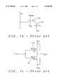
- FIG. 1b illustrates an embedded DRAM cell.
- the embedded DRAM cell has a pass transistor Mp 105 and a cell capacitor C c 102.
- the first plate of the cell capacitor C c 102 is connected to the drain of the pass transistor Mp 105.
- the second plate of the cell capacitor is generally connected to the substrate biasing voltage source V ss .
- the second plate of the cell capacitor may alternatively be connected to a biasing voltage source that is one half the voltage level of the power supply voltage source V DD .
- the source of the pass transistor Mp 105 is connected to a bit line voltage generator V BIT .
- the bit line voltage generator V BIT generates signals that have the appropriate voltage levels that are used to charge or discharge the cell capacitor C c 102.
- the voltage level of the power supply voltage source V DD is used to represent a logical 1 and the ground reference level represents a logical 0.
- the gate of the pass transistor Mp 105 is connected to the word line voltage generator V WORD .
- the word line voltage generator V WORD activates the pass transistor Mp 105 when brought to a voltage level greater than the threshold voltage level Vt of the pass transistor Mp 105. If bit line voltage generator V BIT and thus the source of the pass transistor Mp 105 is at the voltage level of the power supply voltage source V DD , the word line voltage generator has to have a voltage level that is from 1.5-2 times the voltage level of the power supply voltage source.
- FIG. 1c A basic logic circuit is shown in FIG. 1c.
- the N-channel MOS transistor M1 110 and the P-channel MOS transistor M2 115 are configured as a CMOS inverter.
- the inverter can be constructed as a driver or receiver within peripheral circuits of the logic core by appropriate design of the transistor parameters and geometry.
- the structure of a DRAM cell is shown in FIG. 1a.
- the pass transistor Mp 105 is formed on the semiconductor substrate 100 by first implanting an N-type material to a lightly doped concentration into the surface of the substrate 100 to form a deep N-well 125.
- a P-type material is then implanted into the surface of the semiconductor substrate 100 within the area of the deep N-well 125 to form the P-well 130.
- the N-type material is then diffused to highly doped concentration into the P-well 130 to form the source 135 and drain 140 of the pass transistor M p 105.
- the cell capacitor C c 120 is then formed by techniques known in the art, such as stacked capacitor or trench capacitor formation.
- the transistors M1 115 and M2 110 of the logic circuit are formed concurrently with the pass transistor M p 105.
- the N-type material is implanted to the lightly doped concentration to form the N-well 175.
- the N-type material is implanted to a highly doped concentration to form the source 155 and drain 160 of the N-channel transistor 110.
- the P-type material is implanted to a highly doped concentration into the surface of the semiconductor substrate 100 to form the source 180 and the drain 185 of the P-channel MOS transistor 115.
- a thin gate oxide is formed on the surface of the semiconductor substrate 100 in the areas 165 and 190 above the channel region between the source 155 and the drain 160 of the N-channel transistor 110, and the source 180 and the drain 185 of the P-channel transistor 115.
- the gate oxide 145 above the channel between the source 135 and the drain 140 of the pass transistor M p 105 is deposited as a thick gate oxide to prevent excess stress within the thick gate oxide 145. Having multiple thicknesses of the gate oxides 145, 165 and 190 complicates the fabrication process of an ASIC that includes embedded DRAM thus increasing cost. Further, having multiple steps of gate oxide formation causes a higher defect density with the gate oxide.
- the thick oxide is formed to a thickness of from approximately 70 ⁇ to approximately 150 ⁇ , while the thin oxide has a thickness of from approximately 30 ⁇ to approximately 70 ⁇ for the logic circuit and the peripheral circuits.
- the peripheral circuits have a higher operating voltage, and therefore require the thickness of the thin oxide and the thick oxide to be thicker than that of the logic circuit.
- U.S. Pat. No. 5,668,035 discusses a method for fabricating an ASIC with an embedded memory array and a logic core. The method is described for forming a thin gate oxide for the logic core, while providing a thicker oxide for the memory cells having a boosted word line architecture. The method avoids applying photoresist directly to the gate oxide, and thereby prevents contamination.
- a first gate oxide is formed on the device areas on the substrate.
- a first polysilicon layer is deposited and patterned leaving portions over the memory cell areas. The first gate oxide is removed over the logic core areas, and is replaced by a thinner second gate oxide.
- a second polysilicon layer is deposited and patterned to remain over the logic core areas.
- the first and second polysilicon layers having essentially equal thickness, are coated with an insulating layer.
- the FET gate electrodes for both the logic and memory cell areas are simultaneously patterned from the first and second polysilicon layers to complete the DRAM structure up to and including the gate electrodes.
- U.S. Pat. No. 5,702,988 describes a method of forming semiconductor logic devices and memory devices on a single semiconductor substrate.
- the memory devices that may be formed include nonvolatile memory, DRAM and/or SRAM.
- the method begins by forming triple-well structure of N-well regions, P-well regions, and P-well in N-well regions on a semiconductor substrate. Field isolation regions are then formed. A cell is formed for each memory device in the memory regions. A channel implant is performed in the substrate for each of the logic and memory devices. A gate and gate oxide is formed individually for each of the logic and memory devices. LDD (Lightly Doped Drain) active regions and heavily doped source/drain regions are formed adjacent to each gate. Additional memory structures are formed, such as a DRAM capacitor. An interlevel dielectric and contact openings therein are formed. One or more metal layers are subsequently deposited over the interlevel dielectric layer and in the openings to make contact to the contact regions.
- U.S. Pat. No. 5,712,201 (Lee et al.) teaches a semiconductor fabrication process in which both DRAM and logic device structures are integrated on a single silicon chip. The process features combining process steps for both device types, while using only a single level of polysilicon for both a high capacity DRAM cell, as well as for a CMOS logic core.
- the high capacity DRAM cell is composed of an overlying polysilicon storage gate structure, a thin dielectric layer, and an underlying doped semiconductor region.
- U.S. Pat. No. 5,547,893 (Sung) describes a method for simultaneously fabricating memory cells, CMOS devices, and bipolar devices on a semiconductor substrate using a minimum additional number of process steps and process complexity.
- the method of Sung simultaneously fabricates a CMOS DRAM and a vertical bipolar transistor with a low collector resistance and a N+ polysilicon emitter without using an epitaxy layer.
- U.S. Pat. No. 5,600,598 (Skaveland et al.) teaches an embedded DRAM within an ASIC process.
- Skaveland et al. has a structure for storage of charge that avoids charge leakage from the storage capacitor to the substrate, and eliminates the requirement for a continuous voltage V BB .
- the DRAM charge storage structure is comprised of a p-channel access FET in an n - doped well of a p - doped substrate, a p - channel charge storage capacitor, conductive apparatus connecting a plate of the capacitor to a drain of the FET, and apparatus for applying a word line voltage to a gate of the FET.
- Skaveland et al. further teaches a DRAM charge storage structure that is comprised of a charge storage capacitor structure connected between a high voltage source V and a source-drain circuit of a storage cell access FET, the gate of the storage cell access FET being connected to a word line.
- the cell access FET is comprised of first and second p doped regions separated by a channel and contained in an n - doped region of a p - doped substrate.
- the capacitor is comprised of an FET having a gate conductive region insulated from and disposed above the intrinsic n - doped channel region. The gate conductive region of the capacitor is connected to the second p doped region of the FET spaced from the conductive region.
- a third p doped region is contained in the n - doped channel region adjacent the edge of the conductive region.
- An n doped region is contained in the n - doped region spaced from the third p-doped region.
- a high voltage V pp is applied to the n doped region and to the third p doped region.
- the bit line is connected to the first p doped region. Voltage is applied from the word line to a gate of the cell access FET that is boosted from the word line voltage V dd .
- U.S. Pat. No. 5,214,603 (Dhong et al.) teaches a folded bit line DRAM cell that includes a trench capacitor and a planar-configured access transistor. The access transistor is stacked over the capacitor and has a first terminal connected to the capacitor. Dhong et al. further describes a folded bit line DRAM cell that includes a vertically oriented access transistor having one terminal formed on the upper extent of a contact to the trench capacitor, to provide optimum electrical connection to between the access transistor and the contact of the trench capacitor.
- U.S. Pat. No. 5,436,477 (Hashizume et al.) describes a DRAM memory cell where the transfer gate transistors are formed on a main surface of a semiconductor substrate.
- the transfer gate transistors have impurity regions for serving as source/drain regions.
- a first interlayer insulating film having a substantially flat upper surface is formed to cover the transfer gate transistors.
- the first interlayer insulating film is provided with contact holes reaching the impurity regions. Plugs are formed in the contact holes.
- Capacitors are only formed on the flat upper surface of the first interlayer insulating film. Lower electrodes of the capacitors and the plugs are electrically connected with each other through barrier layers.
- Adan U.S. Pat. No. 5,606,189 (Adan) describes a floating electrode capacitor (FEC) DRAM that occupies a small area on the substrate and which nevertheless has a great capacitance.
- Adan provides a dynamic RAM comprising (a) a pair of MOS transistors formed side by side on a substrate, (b) a trench formed in the substrate between Source/Drain active regions A and B adjacent to each other at one end of each of the MOS transistors, and (c) a stack capacitor comprising a first electrode layer connected to the impurity region A, capacitor insulating layer and a second electrode layer connected to the impurity region B the layers being formed one over another and embedded in the trench in the order mentioned.
- An object of this invention is to provide an array of embedded DRAM cells within an ASIC having a pass transistor with a gate oxide having a thickness equal to the thickness of the gate oxide of the logic core.
- an object of this invention to provide an embedded DRAM cell in an array embedded within an ASIC that is activated by signals having voltage levels equal to the voltage levels created by the logic core.
- an embedded DRAM cell is comprised of a cell capacitor to retain digital data as electrical charge and a pass transistor.
- the cell capacitor has a first plate connected to a biasing power supply voltage source.
- the pass transistors has a drain connected to a second plate of the cell capacitor, a source connected to bit line voltage generator, a gate connected to a word line generator, and a gate oxide.
- the gate oxide separates the gate from a channel region that separates the drain from the source.
- the gate oxide has a thickness that is equal to a thickness of gate oxide of either the peripheral circuits or the logic circuits of the logic core of the application specific integrated circuit.
- a signal provided by the word line voltage generator has voltage levels equal to voltage levels of signal provided by peripheral circuits within the logic core.
- a signal provided by the bit line voltage generator has voltage levels equal to voltage levels of signals provided by logic circuits within the logic core.
- the thickness of the gate oxide for the peripheral circuits and thus the gate oxide of the pass transistor is from approximately 30 ⁇ thick to approximately 70 ⁇ thick.
- the signals of the word line voltage generator have a high level of from approximately 3.1 volts to approximately 5.5 volts.
- the signals of the bit line voltage generator have a high level of from approximately 2.3 volts to approximately 2.6 volts.
- a signal provided by the word line voltage generator has voltage levels equal to voltage levels of signals provided by the logic circuits within the logic core.
- the signal provided by the bit line voltage generator has voltage levels equal to voltage levels of signals provided by the logic circuits within the logic core.
- the thickness of the gate oxide for the logic circuits and thus the gate oxide of the pass transistor is from approximately 30 ⁇ thick to approximately 70 ⁇ thick.
- the signals of the word line voltage generator have a high level of from approximately 1.5 volts to approximately 3.3 volts.
- the signals of the bit line voltage generator have a high level of from approximately 1.5 volts to approximately 3.3 volts.
- FIG. 1a is a cross sectional drawing illustrating the embedded DRAM cell and the fundamental logic circuit of an ASIC of the prior art.
- FIG. 1b is a schematic diagram of an embedded DRAM cell of the prior art.
- FIG. 1c is a schematic diagram of the logic circuit within an ASIC of the prior art.
- FIG. 2a is a cross sectional drawing illustrating the embedded DRAM cell and the logic circuit of an ASIC of this invention.
- FIG. 2b is a schematic diagram of an embedded DRAM cell of this invention.
- FIG. 3 is a schematic diagram of embedded DRAM array of this invention.
- the embedded DRAM cell of this invention has a pass transistor M p 205 and cell capacitor C c 220 as shown in FIGS. 2a and 2b.
- An N-type material is implanted into the surface of the semiconductor substrate 200 to a lightly doped concentration to form the deep N-well 225 and the N-well 175.
- a P-type material is then implanted to a lightly doped concentration within the area of the deep N-well 225 to form the P-well 230.
- the N-type material is again implanted into the surface, but to a highly doped concentration to form the source 235 and the drain 240 of the pass transistor M p 205 and the source 155 and drain 160 of the N-channel transistor 110.
- the P-type material is implanted to a highly doped concentration into the surface of semiconductor substrate 200 in the area of the N-well 175 to form the source 185 and drain 180 of the P-channel transistor 115.
- the N-channel transistor 110 and the P-channel transistor 115 form an inverter circuit.
- the inverter circuit is the fundamental circuit of the logic core of the ASIC as described in FIG. 1c.
- a thin gate oxide 245 is formed on the surface of the semiconductor substrate 200 in the channel region between the source 235 and the drain 240 of the pass transistor 205.
- the thin gate oxides 165 and 190 are concurrently formed on the surface of the semiconductor substrate 200 in the channel regions between the source 155 and the drain 160 of the N-channel transistor 110 and the source 185 and the drain 180 of the P-channel transistor 115.
- the thin gate oxides 165 and 195 are fabricated as described in FIG. 1a.
- the thickness of the gate oxide 245 is determined by the voltages of the signals applied to the source 235 by the bit line voltage generator V BIT and to the gate 250 by the word line voltage generator.
- the gate oxide has a thickness of from approximately 30 ⁇ to approximately 70 ⁇ . This thickness is equivalent to the thickness of peripheral circuits of the logic core.
- the voltage level of the signals applied by the bit line voltage generator V BIT to the source 235 of the pass transistor M p 205 are from approximately 1.5 volts to approximately 3.3 volts. These signal levels are equivalent to the signal levels of the logic circuits of the logic core.
- the voltage levels of signals applied by the word line voltage generator V WORD to the gate 250 of the pass transistor M p 205 is from approximately 1.5 volts to approximately 3.3 volts. These signal levels are equivalent to the signal levels of the peripheral circuits of the logic core.
- the second embodiment of this invention has a gate oxide thickness of from approximately 30 ⁇ to approximately 70 ⁇ . This thickness is equivalent to the thickness of the gate oxide of the logic circuits or the logic core.
- the voltage level of signals applied by the bit line voltage generator V BIT to the source 235 of the pass transistor M p 205 are from approximately 1.5 volts to approximately 3.3 volts. This voltage is equivalent to the voltage levels of the logic circuitry.
- the capacitance of the cell capacitor C c 220 must be increased or the number of cell capacitors C c 220 present on each bit line of an array as shown in FIG. 3 is decreased to allow the transfer of the charge representing the digital data to the bit line to be sufficient to be detected by the sense amplifier of the array.
- the voltage levels of the signals applied by the word line voltage generator V WORD are from approximately 1.5 Volts to approximately 3.3 volts. This voltage level is equivalent to the voltage levels of the logic circuitry of the logic core.
- the thinner gate oxide 245 will have a lower defect density since extra steps are not required to form the gate oxide 245.
- the embedded array of DRAM cells has multiple DRAM cells, CELL 11 400, CELL 12 402, CELL 13 404, CELL 14, 406, CELL 21 408, and CELL 31 410 arranged rows and columns.
- the bit line voltage generator V BIT 0 412 is connected to the bit line 420 which is connected to the sources of the pass transistors M p of the column of embedded DRAM cells CELL 11 400, CELL 21 408, and CELL 31 410.
- the sources of the pass transistors M p of the embedded DRAM cells CELL 12 402, CELL 13 404, and CELL 14 406 are respectively connected to the bit line voltage generators V BIT 1 414, V BIT 2 416, V BIT 3 418.
- the word line voltage generator V WORD 0 428 is connected to the gates of the pass transistor of the row of the embedded DRAM cells CELL 11 400, CELL 12 402, CELL 13 404, and CELL 14, 406. Likewise, the word line voltage generators V WORD 1 430 and V WORD 2 432 are respectively connected to the gates of the pass transistor M p of embedded DRAM cells CELL 21 408 and CELL 31 410.
- the bias voltage source V B is connected to the second plate of the cell capacitor C c of the embedded DRAM cell CELL 11 400, CELL 12 402, CELL 13 404, CELL 14, 406, CELL 21 408, and CELL 31 410 to provide the back bias for the cell capacitors C c .
- the bias voltage source V B is held to a constant voltage that is one half the voltage level of the power supply voltage source V DD .
- Each of the bit lines 420, 422, 424, and 426 is connected to the sense amplifiers SA1 440, SA2 442, SA3 444, and SA4 446.
- the sense amplifiers SA1 440, SA2 442, SA3 444, and SA4 446 detect the level of a charge present of a selected embedded DRAM cell from the embedded array of DRAM cells.
- Each of the bit line voltage generators V BIT 0 412, V BIT 1 414, V BIT 2 416, and V BIT 3 418 will create signals having voltage levels of the logic circuits of the logic core if the pass transistor M p of the embedded DRAM cells CELL 11 400, CELL 12 402, CELL 13 404, CELL 14, 406, CELL 21 408, and CELL 31 410 have a gate oxide thickness of the peripheral circuits of the logic core.
- each of the bit line generators V BIT 0 412, V BIT 1 414, V BIT 2 416, and V BIT 3 418 will create signals having voltage levels of the logic circuits less the differential voltage described above of the logic core, if the pass transistors M p of the of the embedded DRAM cells CELL 11 400, CELL 12 402, CELL 13 404, CELL 14, 406, CELL 21 408, and CELL 31 410 have a gate oxide thickness of the peripheral circuits of the logic core.
- Each of the word line voltage generators V WORD 0 428, V WORD 1 430, and V WORD 2 432 will create signals having voltage levels of the peripheral circuits of the logic core as described above, if the pass transistors M p of the embedded DRAM cells CELL 11 400, CELL 12 402, CELL 13 404, CELL 14, 406, CELL 21 408, and CELL 31 410 have a gate oxide thickness of the peripheral circuits of the logic core.
- each of the word line generators V WORD 0 428, V WORD 1 430, and V WORD 2 432 will create signals having voltage levels of the logic circuits of the logic core as described above, if the pass transistor M p of the embedded DRAM cells CELL 11 400, CELL 12 402, CELL 13 404, CELL 14, 406, CELL 21 408, and CELL 31 410 have a gate oxide thickness of the logic circuits of the logic core.
- the N-well 175 of FIG. 2a can be expanded to incorporate the source 155 and the drain 160 of the N-channel transistor 110.
- This "triple well" construction will require an implantation of the P-type material to a lightly doped concentration in the region of P-channel 110.
- the structure of the logic core will more closely resemble that of the pass transistor M p 205 of embedded DRAM cell.
Abstract
Embedded DRAM cells within an ASIC having a pass transistor with a gate oxide having a thickness equal to the thickness of the gate oxide of the logic core. This allows the embedded DRAM cell to be activated by signals having voltage levels equal to the voltage levels created by the logic core. If the gate oxide has a thickness that is equal to the gate oxide thickness of the peripheral circuits, a signal provided by the word line voltage generator has voltage levels equal to those provided by peripheral circuits, and signal provided by the bit line voltage generator has voltage levels equal to those provided by logic circuits within the logic core. If the gate oxide has a thickness that is equal to the thickness of the gate oxide of the logic circuits, a signal provided by the word line voltage generator has voltage levels equal to those provided by the logic circuits, and the bit line voltage generator has voltage levels equal to those provided by the logic circuits.
Description
1. Field of the Invention
This invention relates to integrated circuits containing logic circuits and embedded Dynamic Random Access Memory (DRAM). More particularly, this invention relates structures of pass transistors within the embedded DRAM such that the processing of the pass transistor is equivalent to that of transistors that form the logic core.
2. Description of the Related Art
Application Specific Integrated Circuits (ASIC) contain sections of circuitry that implement digital logic, provide peripheral circuits to interface to system function, memory, and analog functions. As DRAM has been embedded into an ASIC, the process for constructing the ASIC has become more complex.
Refer now to FIGS. 1a, 1b, and 1c for discussion of the structure of an ASIC containing a logic core and an embedded DRAM array. FIG. 1b illustrates an embedded DRAM cell. The embedded DRAM cell has a pass transistor Mp 105 and a cell capacitor Cc 102. The first plate of the cell capacitor Cc 102 is connected to the drain of the pass transistor Mp 105. The second plate of the cell capacitor is generally connected to the substrate biasing voltage source Vss. The second plate of the cell capacitor may alternatively be connected to a biasing voltage source that is one half the voltage level of the power supply voltage source VDD.
The source of the pass transistor Mp 105 is connected to a bit line voltage generator VBIT. The bit line voltage generator VBIT generates signals that have the appropriate voltage levels that are used to charge or discharge the cell capacitor Cc 102. Generally the voltage level of the power supply voltage source VDD is used to represent a logical 1 and the ground reference level represents a logical 0.
The gate of the pass transistor Mp 105 is connected to the word line voltage generator VWORD. The word line voltage generator VWORD activates the pass transistor Mp 105 when brought to a voltage level greater than the threshold voltage level Vt of the pass transistor Mp 105. If bit line voltage generator VBIT and thus the source of the pass transistor Mp 105 is at the voltage level of the power supply voltage source VDD, the word line voltage generator has to have a voltage level that is from 1.5-2 times the voltage level of the power supply voltage source.
A basic logic circuit is shown in FIG. 1c. The N-channel MOS transistor M1 110 and the P-channel MOS transistor M2 115 are configured as a CMOS inverter. By appropriate placement of additional N-channel and P-channel MOS transistors within the circuit, more complex logic functions can be created. Further, the inverter can be constructed as a driver or receiver within peripheral circuits of the logic core by appropriate design of the transistor parameters and geometry.
The structure of a DRAM cell is shown in FIG. 1a. The pass transistor Mp 105 is formed on the semiconductor substrate 100 by first implanting an N-type material to a lightly doped concentration into the surface of the substrate 100 to form a deep N-well 125. A P-type material is then implanted into the surface of the semiconductor substrate 100 within the area of the deep N-well 125 to form the P-well 130. The N-type material is then diffused to highly doped concentration into the P-well 130 to form the source 135 and drain 140 of the pass transistor M p 105.
The cell capacitor C c 120 is then formed by techniques known in the art, such as stacked capacitor or trench capacitor formation.
The transistors M1 115 and M2 110 of the logic circuit are formed concurrently with the pass transistor M p 105. The N-type material is implanted to the lightly doped concentration to form the N-well 175. The N-type material is implanted to a highly doped concentration to form the source 155 and drain 160 of the N-channel transistor 110.
The P-type material is implanted to a highly doped concentration into the surface of the semiconductor substrate 100 to form the source 180 and the drain 185 of the P-channel MOS transistor 115.
A thin gate oxide is formed on the surface of the semiconductor substrate 100 in the areas 165 and 190 above the channel region between the source 155 and the drain 160 of the N-channel transistor 110, and the source 180 and the drain 185 of the P-channel transistor 115.
Since the voltage level of the word line voltage generator VWORD is as much as twice the voltage level of the power supply voltage source VDD, the gate oxide 145 above the channel between the source 135 and the drain 140 of the pass transistor M p 105 is deposited as a thick gate oxide to prevent excess stress within the thick gate oxide 145. Having multiple thicknesses of the gate oxides 145, 165 and 190 complicates the fabrication process of an ASIC that includes embedded DRAM thus increasing cost. Further, having multiple steps of gate oxide formation causes a higher defect density with the gate oxide.
Typically, the thick oxide is formed to a thickness of from approximately 70 Å to approximately 150 Å, while the thin oxide has a thickness of from approximately 30 Å to approximately 70 Å for the logic circuit and the peripheral circuits. Generally the peripheral circuits have a higher operating voltage, and therefore require the thickness of the thin oxide and the thick oxide to be thicker than that of the logic circuit.
U.S. Pat. No. 5,668,035 (Fang et al.) discusses a method for fabricating an ASIC with an embedded memory array and a logic core. The method is described for forming a thin gate oxide for the logic core, while providing a thicker oxide for the memory cells having a boosted word line architecture. The method avoids applying photoresist directly to the gate oxide, and thereby prevents contamination. A first gate oxide is formed on the device areas on the substrate. A first polysilicon layer is deposited and patterned leaving portions over the memory cell areas. The first gate oxide is removed over the logic core areas, and is replaced by a thinner second gate oxide. A second polysilicon layer is deposited and patterned to remain over the logic core areas. The first and second polysilicon layers, having essentially equal thickness, are coated with an insulating layer. The FET gate electrodes for both the logic and memory cell areas are simultaneously patterned from the first and second polysilicon layers to complete the DRAM structure up to and including the gate electrodes.
U.S. Pat. No. 5,702,988 (Liang) describes a method of forming semiconductor logic devices and memory devices on a single semiconductor substrate. The memory devices that may be formed include nonvolatile memory, DRAM and/or SRAM. The method begins by forming triple-well structure of N-well regions, P-well regions, and P-well in N-well regions on a semiconductor substrate. Field isolation regions are then formed. A cell is formed for each memory device in the memory regions. A channel implant is performed in the substrate for each of the logic and memory devices. A gate and gate oxide is formed individually for each of the logic and memory devices. LDD (Lightly Doped Drain) active regions and heavily doped source/drain regions are formed adjacent to each gate. Additional memory structures are formed, such as a DRAM capacitor. An interlevel dielectric and contact openings therein are formed. One or more metal layers are subsequently deposited over the interlevel dielectric layer and in the openings to make contact to the contact regions.
U.S. Pat. No. 5,712,201 (Lee et al.) teaches a semiconductor fabrication process in which both DRAM and logic device structures are integrated on a single silicon chip. The process features combining process steps for both device types, while using only a single level of polysilicon for both a high capacity DRAM cell, as well as for a CMOS logic core. The high capacity DRAM cell is composed of an overlying polysilicon storage gate structure, a thin dielectric layer, and an underlying doped semiconductor region.
U.S. Pat. No. 5,547,893 (Sung) describes a method for simultaneously fabricating memory cells, CMOS devices, and bipolar devices on a semiconductor substrate using a minimum additional number of process steps and process complexity. The method of Sung simultaneously fabricates a CMOS DRAM and a vertical bipolar transistor with a low collector resistance and a N+ polysilicon emitter without using an epitaxy layer.
U.S. Pat. No. 5,600,598 (Skaveland et al.) teaches an embedded DRAM within an ASIC process. Skaveland et al. has a structure for storage of charge that avoids charge leakage from the storage capacitor to the substrate, and eliminates the requirement for a continuous voltage VBB. The DRAM charge storage structure is comprised of a p-channel access FET in an n- doped well of a p- doped substrate, a p- channel charge storage capacitor, conductive apparatus connecting a plate of the capacitor to a drain of the FET, and apparatus for applying a word line voltage to a gate of the FET.
Skaveland et al. further teaches a DRAM charge storage structure that is comprised of a charge storage capacitor structure connected between a high voltage source V and a source-drain circuit of a storage cell access FET, the gate of the storage cell access FET being connected to a word line. The cell access FET is comprised of first and second p doped regions separated by a channel and contained in an n- doped region of a p- doped substrate. The capacitor is comprised of an FET having a gate conductive region insulated from and disposed above the intrinsic n- doped channel region. The gate conductive region of the capacitor is connected to the second p doped region of the FET spaced from the conductive region. A third p doped region is contained in the n- doped channel region adjacent the edge of the conductive region. An n doped region is contained in the n- doped region spaced from the third p-doped region. A high voltage Vpp is applied to the n doped region and to the third p doped region. The bit line is connected to the first p doped region. Voltage is applied from the word line to a gate of the cell access FET that is boosted from the word line voltage Vdd.
U.S. Pat. No. 5,214,603 (Dhong et al.) teaches a folded bit line DRAM cell that includes a trench capacitor and a planar-configured access transistor. The access transistor is stacked over the capacitor and has a first terminal connected to the capacitor. Dhong et al. further describes a folded bit line DRAM cell that includes a vertically oriented access transistor having one terminal formed on the upper extent of a contact to the trench capacitor, to provide optimum electrical connection to between the access transistor and the contact of the trench capacitor.
U.S. Pat. No. 5,436,477 (Hashizume et al.) describes a DRAM memory cell where the transfer gate transistors are formed on a main surface of a semiconductor substrate. The transfer gate transistors have impurity regions for serving as source/drain regions. A first interlayer insulating film having a substantially flat upper surface is formed to cover the transfer gate transistors. The first interlayer insulating film is provided with contact holes reaching the impurity regions. Plugs are formed in the contact holes. Capacitors are only formed on the flat upper surface of the first interlayer insulating film. Lower electrodes of the capacitors and the plugs are electrically connected with each other through barrier layers.
U.S. Pat. No. 5,606,189 (Adan) describes a floating electrode capacitor (FEC) DRAM that occupies a small area on the substrate and which nevertheless has a great capacitance. Adan provides a dynamic RAM comprising (a) a pair of MOS transistors formed side by side on a substrate, (b) a trench formed in the substrate between Source/Drain active regions A and B adjacent to each other at one end of each of the MOS transistors, and (c) a stack capacitor comprising a first electrode layer connected to the impurity region A, capacitor insulating layer and a second electrode layer connected to the impurity region B the layers being formed one over another and embedded in the trench in the order mentioned.
An object of this invention is to provide an array of embedded DRAM cells within an ASIC having a pass transistor with a gate oxide having a thickness equal to the thickness of the gate oxide of the logic core.
Further, it is an object of this invention to provide an embedded DRAM cell in an array embedded within an ASIC that is activated by signals having voltage levels equal to the voltage levels created by the logic core.
To accomplish these and other objects an embedded DRAM cell is comprised of a cell capacitor to retain digital data as electrical charge and a pass transistor. The cell capacitor has a first plate connected to a biasing power supply voltage source. The pass transistors has a drain connected to a second plate of the cell capacitor, a source connected to bit line voltage generator, a gate connected to a word line generator, and a gate oxide. The gate oxide separates the gate from a channel region that separates the drain from the source. The gate oxide has a thickness that is equal to a thickness of gate oxide of either the peripheral circuits or the logic circuits of the logic core of the application specific integrated circuit.
If the gate oxide has a thickness that is equal to the gate oxide thickness of the peripheral circuits of the logic core, a signal provided by the word line voltage generator has voltage levels equal to voltage levels of signal provided by peripheral circuits within the logic core. A signal provided by the bit line voltage generator has voltage levels equal to voltage levels of signals provided by logic circuits within the logic core. The thickness of the gate oxide for the peripheral circuits and thus the gate oxide of the pass transistor is from approximately 30 Å thick to approximately 70 Å thick.
The signals of the word line voltage generator have a high level of from approximately 3.1 volts to approximately 5.5 volts. The signals of the bit line voltage generator have a high level of from approximately 2.3 volts to approximately 2.6 volts.
However, if the gate oxide has a thickness that is equal to the thickness of the gate oxide of the logic circuits, a signal provided by the word line voltage generator has voltage levels equal to voltage levels of signals provided by the logic circuits within the logic core. The signal provided by the bit line voltage generator has voltage levels equal to voltage levels of signals provided by the logic circuits within the logic core. The thickness of the gate oxide for the logic circuits and thus the gate oxide of the pass transistor is from approximately 30 Å thick to approximately 70 Å thick.
The signals of the word line voltage generator have a high level of from approximately 1.5 volts to approximately 3.3 volts. The signals of the bit line voltage generator have a high level of from approximately 1.5 volts to approximately 3.3 volts.
FIG. 1a is a cross sectional drawing illustrating the embedded DRAM cell and the fundamental logic circuit of an ASIC of the prior art.
FIG. 1b is a schematic diagram of an embedded DRAM cell of the prior art.
FIG. 1c is a schematic diagram of the logic circuit within an ASIC of the prior art.
FIG. 2a is a cross sectional drawing illustrating the embedded DRAM cell and the logic circuit of an ASIC of this invention.
FIG. 2b is a schematic diagram of an embedded DRAM cell of this invention.
FIG. 3 is a schematic diagram of embedded DRAM array of this invention.
The embedded DRAM cell of this invention has a pass transistor M p 205 and cell capacitor C c 220 as shown in FIGS. 2a and 2b. An N-type material is implanted into the surface of the semiconductor substrate 200 to a lightly doped concentration to form the deep N-well 225 and the N-well 175. A P-type material is then implanted to a lightly doped concentration within the area of the deep N-well 225 to form the P-well 230.
The N-type material is again implanted into the surface, but to a highly doped concentration to form the source 235 and the drain 240 of the pass transistor M p 205 and the source 155 and drain 160 of the N-channel transistor 110.
The P-type material is implanted to a highly doped concentration into the surface of semiconductor substrate 200 in the area of the N-well 175 to form the source 185 and drain 180 of the P-channel transistor 115.
The N-channel transistor 110 and the P-channel transistor 115 form an inverter circuit. The inverter circuit is the fundamental circuit of the logic core of the ASIC as described in FIG. 1c.
A thin gate oxide 245 is formed on the surface of the semiconductor substrate 200 in the channel region between the source 235 and the drain 240 of the pass transistor 205. The thin gate oxides 165 and 190 are concurrently formed on the surface of the semiconductor substrate 200 in the channel regions between the source 155 and the drain 160 of the N-channel transistor 110 and the source 185 and the drain 180 of the P-channel transistor 115. The thin gate oxides 165 and 195 are fabricated as described in FIG. 1a.
The thickness of the gate oxide 245 is determined by the voltages of the signals applied to the source 235 by the bit line voltage generator VBIT and to the gate 250 by the word line voltage generator.
In the first embodiment of this invention, the gate oxide has a thickness of from approximately 30 Å to approximately 70 Å. This thickness is equivalent to the thickness of peripheral circuits of the logic core. The voltage level of the signals applied by the bit line voltage generator VBIT to the source 235 of the pass transistor M p 205 are from approximately 1.5 volts to approximately 3.3 volts. These signal levels are equivalent to the signal levels of the logic circuits of the logic core. The voltage levels of signals applied by the word line voltage generator VWORD to the gate 250 of the pass transistor M p 205 is from approximately 1.5 volts to approximately 3.3 volts. These signal levels are equivalent to the signal levels of the peripheral circuits of the logic core.
The second embodiment of this invention has a gate oxide thickness of from approximately 30 Å to approximately 70 Å. This thickness is equivalent to the thickness of the gate oxide of the logic circuits or the logic core.
The voltage level of signals applied by the bit line voltage generator VBIT to the source 235 of the pass transistor M p 205 are from approximately 1.5 volts to approximately 3.3 volts. This voltage is equivalent to the voltage levels of the logic circuitry.
The capacitance of the cell capacitor C c 220 must be increased or the number of cell capacitors C c 220 present on each bit line of an array as shown in FIG. 3 is decreased to allow the transfer of the charge representing the digital data to the bit line to be sufficient to be detected by the sense amplifier of the array.
The voltage levels of the signals applied by the word line voltage generator VWORD are from approximately 1.5 Volts to approximately 3.3 volts. This voltage level is equivalent to the voltage levels of the logic circuitry of the logic core.
By having the voltage levels that activate the pass transistor M p 205 equal to the voltage levels of either the peripheral circuits or the logic circuits of the logic core, there is no added complexity for the process to fabricate the transistors of the ASIC including the embedded Dram than for the ASIC containing only a logic core. Further, the thinner gate oxide 245 will have a lower defect density since extra steps are not required to form the gate oxide 245.
Refer now to FIG. 3 for a discussion of an embedded array of DRAM cells within an ASIC. The embedded array of DRAM cells has multiple DRAM cells, CELL 11 400, CELL 12 402, CELL 13 404, CELL 14, 406, CELL 21 408, and CELL 31 410 arranged rows and columns. The bit line voltage generator VBIT 0 412 is connected to the bit line 420 which is connected to the sources of the pass transistors Mp of the column of embedded DRAM cells CELL 11 400, CELL 21 408, and CELL 31 410. Likewise, the sources of the pass transistors Mp of the embedded DRAM cells CELL 12 402, CELL 13 404, and CELL 14 406 are respectively connected to the bit line voltage generators V BIT 1 414, V BIT 2 416, V BIT 3 418.
The word line voltage generator VWORD 0 428 is connected to the gates of the pass transistor of the row of the embedded DRAM cells CELL 11 400, CELL 12 402, CELL 13 404, and CELL 14, 406. Likewise, the word line voltage generators V WORD 1 430 and V WORD 2 432 are respectively connected to the gates of the pass transistor Mp of embedded DRAM cells CELL 21 408 and CELL 31 410.
The bias voltage source VB is connected to the second plate of the cell capacitor Cc of the embedded DRAM cell CELL 11 400, CELL 12 402, CELL 13 404, CELL 14, 406, CELL 21 408, and CELL 31 410 to provide the back bias for the cell capacitors Cc. The bias voltage source VB is held to a constant voltage that is one half the voltage level of the power supply voltage source VDD.
Each of the bit lines 420, 422, 424, and 426 is connected to the sense amplifiers SA1 440, SA2 442, SA3 444, and SA4 446. The sense amplifiers SA1 440, SA2 442, SA3 444, and SA4 446 detect the level of a charge present of a selected embedded DRAM cell from the embedded array of DRAM cells.
Each of the bit line voltage generators VBIT 0 412, V BIT 1 414, V BIT 2 416, and V BIT 3 418 will create signals having voltage levels of the logic circuits of the logic core if the pass transistor Mp of the embedded DRAM cells CELL 11 400, CELL 12 402, CELL 13 404, CELL 14, 406, CELL 21 408, and CELL 31 410 have a gate oxide thickness of the peripheral circuits of the logic core. However, each of the bit line generators VBIT 0 412, V BIT 1 414, V BIT 2 416, and V BIT 3 418 will create signals having voltage levels of the logic circuits less the differential voltage described above of the logic core, if the pass transistors Mp of the of the embedded DRAM cells CELL 11 400, CELL 12 402, CELL 13 404, CELL 14, 406, CELL 21 408, and CELL 31 410 have a gate oxide thickness of the peripheral circuits of the logic core.
Each of the word line voltage generators VWORD 0 428, V WORD 1 430, and V WORD 2 432 will create signals having voltage levels of the peripheral circuits of the logic core as described above, if the pass transistors Mp of the embedded DRAM cells CELL 11 400, CELL 12 402, CELL 13 404, CELL 14, 406, CELL 21 408, and CELL 31 410 have a gate oxide thickness of the peripheral circuits of the logic core. However, each of the word line generators VWORD 0 428, V WORD 1 430, and V WORD 2 432 will create signals having voltage levels of the logic circuits of the logic core as described above, if the pass transistor Mp of the embedded DRAM cells CELL 11 400, CELL 12 402, CELL 13 404, CELL 14, 406, CELL 21 408, and CELL 31 410 have a gate oxide thickness of the logic circuits of the logic core.
It is well known in the art that the N-well 175 of FIG. 2a can be expanded to incorporate the source 155 and the drain 160 of the N-channel transistor 110. This "triple well" construction will require an implantation of the P-type material to a lightly doped concentration in the region of P-channel 110. Thus, the structure of the logic core will more closely resemble that of the pass transistor M p 205 of embedded DRAM cell.
While this invention has been particularly shown and described with reference to the preferred embodiments thereof, it will be understood by those skilled in the art that various changes in form and details may be made without departing from the spirit and scope of the invention.
Claims (13)
1. A method of forming an application specific integrated circuit containing an array of embedded DRAM cells and a logic core on a semiconductor substrate of a first conductivity type, comprising the steps of:
implanting a material of a second conductivity type into the surface of the semiconductor substrate to a lightly doped concentration to form primary wells;
implanting the material of the first conductivity type into the surface of the semiconductor substrate to a lightly doped concentration to form secondary wells within the primary wells in locations of said application specific integrated circuit containing the array of embedded DRAM cells;
implanting the material of the second conductivity type into the surface of the semiconductor substrate to a highly doped concentration to form sources and drains of transistors of a first channel type including a pass transistor of each embedded DRAM cell;
implanting the material of the first conductivity type to a highly doped concentration to form sources and drains of transistors of a second channel type;
forming a cell capacitor for each embedded DRAM cell;
forming a gate oxide over the channel area between the source and drain of transistors of logic circuits within the logic core;
forming a gate oxide over the channel area between the source and drains of transistors of peripheral circuits within the logic core;
forming a gate oxide over a channel area between the source and drain of each pass transistor of each embedded DRAM cell whereby a thickness of the gate oxide of the pass transistor of each embedded DRAM cell is equal to the thickness of the transistors of the logic core;
forming gate electrodes on the gate oxide of the pass transistors and the transistors of the logic core;
connecting a plurality of word line voltage generators to rows of pass transistors within the array of embedded DRAM cells; and
connecting a plurality of bit line voltage generators to columns of pass transistors within the array of embedded DRAM cells.
2. The method of claim 1 wherein a signal provided by each word line voltage generator has voltage levels equal to voltage levels of signal provided by peripheral circuits within said logic core.
3. The method of claim 2 wherein the thickness of the gate oxide is equal to the thickness of the gate oxide of the peripheral circuits within the logic core.
4. The method of claim 2 wherein a signal provided by each bit line voltage generator has voltage levels equal to voltage levels of signals provided by logic circuits within said logic core.
5. The method of claim 1 wherein the signal provided by each word line voltage generator has voltage levels equal to voltage levels of signals provided by the logic circuits within said logic core.
6. The method of claim 5 wherein the thickness of the gate oxide is equal to the thickness of the gate oxide of the logic circuits within said logic core.
7. The method of claim 6 wherein the signal provided by each bit line voltage generator has voltage levels equal to voltage levels of signals provided by the logic circuits within said logic core.
8. The method of claim 3 wherein the thickness of the gate oxide is from approximately 30 Å thick to approximately 70 Å thick.
9. The method of claim 6 wherein the thickness of the gate oxide is from approximately 30 Å thick to approximately 70 Å thick.
10. The method of claim 2 wherein the signals of each word line voltage generator have a high level of from approximately 1.5 volts to approximately 3.3 volts.
11. The method of claim 4 wherein the signals of each bit line voltage generator have a high level of from approximately 1.5 volts to approximately 3.3 volts.
12. The method of claim 5 wherein the signals of each word line voltage generator have a high level of from 1.5 volts to approximately 3.3 volts.
13. The method of claim 7 wherein the signals of each bit line voltage generator have a high level of from approximately 1.5 volts to approximately 3.3 volts.
Priority Applications (2)
| Application Number | Priority Date | Filing Date | Title |
|---|---|---|---|
| US09/195,653 US6136638A (en) | 1998-11-19 | 1998-11-19 | Process technology architecture of embedded DRAM |
| US09/670,328 US6600186B1 (en) | 1998-11-19 | 2000-09-27 | Process technology architecture of embedded DRAM |
Applications Claiming Priority (1)
| Application Number | Priority Date | Filing Date | Title |
|---|---|---|---|
| US09/195,653 US6136638A (en) | 1998-11-19 | 1998-11-19 | Process technology architecture of embedded DRAM |
Related Child Applications (1)
| Application Number | Title | Priority Date | Filing Date |
|---|---|---|---|
| US09/670,328 Division US6600186B1 (en) | 1998-11-19 | 2000-09-27 | Process technology architecture of embedded DRAM |
Publications (1)
| Publication Number | Publication Date |
|---|---|
| US6136638A true US6136638A (en) | 2000-10-24 |
Family
ID=22722211
Family Applications (2)
| Application Number | Title | Priority Date | Filing Date |
|---|---|---|---|
| US09/195,653 Expired - Lifetime US6136638A (en) | 1998-11-19 | 1998-11-19 | Process technology architecture of embedded DRAM |
| US09/670,328 Expired - Lifetime US6600186B1 (en) | 1998-11-19 | 2000-09-27 | Process technology architecture of embedded DRAM |
Family Applications After (1)
| Application Number | Title | Priority Date | Filing Date |
|---|---|---|---|
| US09/670,328 Expired - Lifetime US6600186B1 (en) | 1998-11-19 | 2000-09-27 | Process technology architecture of embedded DRAM |
Country Status (1)
| Country | Link |
|---|---|
| US (2) | US6136638A (en) |
Cited By (11)
| Publication number | Priority date | Publication date | Assignee | Title |
|---|---|---|---|---|
| US6261894B1 (en) * | 2000-11-03 | 2001-07-17 | International Business Machines Corporation | Method for forming dual workfunction high-performance support MOSFETs in EDRAM arrays |
| US6400626B1 (en) * | 1999-09-24 | 2002-06-04 | Clearspeed Technology Limited | Memory devices |
| US20020163935A1 (en) * | 2001-05-04 | 2002-11-07 | Terago Communications, Inc. | System and method for providing transformation of multi-protocol packets in a data stream |
| US20020163909A1 (en) * | 2001-05-04 | 2002-11-07 | Terago Communications, Inc. | Method and apparatus for providing multi-protocol, multi-stage, real-time frame classification |
| US20050036363A1 (en) * | 1996-05-24 | 2005-02-17 | Jeng-Jye Shau | High performance embedded semiconductor memory devices with multiple dimension first-level bit-lines |
| US20050133852A1 (en) * | 1996-05-24 | 2005-06-23 | Jeng-Jye Shau | High performance embedded semiconductor memory devices with multiple dimension first-level bit-lines |
| US20050195855A1 (en) * | 2001-05-04 | 2005-09-08 | Slt Logic Llc | System and method for policing multiple data flows and multi-protocol data flows |
| US20060087969A1 (en) * | 2001-05-04 | 2006-04-27 | Slt Logic Llc | System and method for hierarchical policing of flows and subflows of a data stream |
| US20070168829A1 (en) * | 1996-05-24 | 2007-07-19 | Jeng-Jye Shau | Methods to make DRAM fully compatible with SRAM |
| US20080116496A1 (en) * | 2006-11-21 | 2008-05-22 | Kuo-Chyuan Tzeng | Integrating a DRAM with an SRAM having butted contacts and resulting devices |
| US20100187587A1 (en) * | 2009-01-28 | 2010-07-29 | Chartered Semiconductor Manufacturing, Ltd. | Memory cell structure and method for fabrication thereof |
Families Citing this family (9)
| Publication number | Priority date | Publication date | Assignee | Title |
|---|---|---|---|---|
| US6532018B1 (en) * | 1999-04-19 | 2003-03-11 | Microsoft Corporation | Combined floating-point logic core and frame buffer |
| US7141468B2 (en) * | 2003-10-27 | 2006-11-28 | Texas Instruments Incorporated | Application of different isolation schemes for logic and embedded memory |
| US7095094B2 (en) * | 2004-09-29 | 2006-08-22 | Agere Systems Inc. | Multiple doping level bipolar junctions transistors and method for forming |
| US7499307B2 (en) * | 2005-06-24 | 2009-03-03 | Mosys, Inc. | Scalable embedded DRAM array |
| US7274618B2 (en) * | 2005-06-24 | 2007-09-25 | Monolithic System Technology, Inc. | Word line driver for DRAM embedded in a logic process |
| US8384155B2 (en) * | 2006-07-18 | 2013-02-26 | Ememory Technology Inc. | Semiconductor capacitor |
| US8754498B2 (en) * | 2009-10-27 | 2014-06-17 | Taiwan Semiconductor Manufacturing Co., Ltd. | Antifuse and method of making the antifuse |
| US8455936B2 (en) * | 2010-02-25 | 2013-06-04 | Avago Technologies General Ip (Singapore) Pte. Ltd. | Configurable memory sheet and package assembly |
| US8609457B2 (en) | 2011-05-03 | 2013-12-17 | Globalfoundries Inc. | Semiconductor device with DRAM bit lines made from same material as gate electrodes in non-memory regions of the device, and methods of making same |
Citations (11)
| Publication number | Priority date | Publication date | Assignee | Title |
|---|---|---|---|---|
| US5214603A (en) * | 1991-08-05 | 1993-05-25 | International Business Machines Corporation | Folded bitline, ultra-high density dynamic random access memory having access transistors stacked above trench storage capacitors |
| US5238860A (en) * | 1987-07-10 | 1993-08-24 | Kabushiki Kaisha Toshiba | Semiconductor device having different impurity concentration wells |
| US5436477A (en) * | 1993-06-24 | 1995-07-25 | Mitsubishi Denki Kabushiki Kaisha | Semiconductor memory device with high dielectric capacitor structure |
| US5547893A (en) * | 1995-12-27 | 1996-08-20 | Vanguard International Semiconductor Corp. | method for fabricating an embedded vertical bipolar transistor and a memory cell |
| US5600598A (en) * | 1994-12-14 | 1997-02-04 | Mosaid Technologies Incorporated | Memory cell and wordline driver for embedded DRAM in ASIC process |
| US5606189A (en) * | 1991-03-13 | 1997-02-25 | Sharp Kabushiki Kaisha | Dynamic RAM trench capacitor device with contact strap |
| US5668035A (en) * | 1996-06-10 | 1997-09-16 | Taiwan Semiconductor Manufacturing Company Ltd. | Method for fabricating a dual-gate dielectric module for memory with embedded logic technology |
| US5702988A (en) * | 1996-05-02 | 1997-12-30 | Taiwan Semiconductor Manufacturing Company, Ltd. | Blending integrated circuit technology |
| US5712201A (en) * | 1996-06-07 | 1998-01-27 | Taiwan Semiconductor Manufacturing Company, Ltd. | Fabrication method for integrating logic and single level polysilicon DRAM devices on the same semiconductor chip |
| US5789788A (en) * | 1993-11-22 | 1998-08-04 | Fujitsu Limited | Semiconductor device with first and second wells which have opposite conductivity types and a third well region formed on one of the first and second wells |
| US5872032A (en) * | 1997-11-03 | 1999-02-16 | Vanguard International Semiconductor Corporation | Fabrication method for a DRAM cell with bipolar charge amplification |
Family Cites Families (2)
| Publication number | Priority date | Publication date | Assignee | Title |
|---|---|---|---|---|
| JPH07142597A (en) * | 1993-11-12 | 1995-06-02 | Mitsubishi Electric Corp | Semiconductor memory device and manufacture thereof |
| JP2765544B2 (en) * | 1995-12-26 | 1998-06-18 | 日本電気株式会社 | Method for manufacturing semiconductor device |
-
1998
- 1998-11-19 US US09/195,653 patent/US6136638A/en not_active Expired - Lifetime
-
2000
- 2000-09-27 US US09/670,328 patent/US6600186B1/en not_active Expired - Lifetime
Patent Citations (11)
| Publication number | Priority date | Publication date | Assignee | Title |
|---|---|---|---|---|
| US5238860A (en) * | 1987-07-10 | 1993-08-24 | Kabushiki Kaisha Toshiba | Semiconductor device having different impurity concentration wells |
| US5606189A (en) * | 1991-03-13 | 1997-02-25 | Sharp Kabushiki Kaisha | Dynamic RAM trench capacitor device with contact strap |
| US5214603A (en) * | 1991-08-05 | 1993-05-25 | International Business Machines Corporation | Folded bitline, ultra-high density dynamic random access memory having access transistors stacked above trench storage capacitors |
| US5436477A (en) * | 1993-06-24 | 1995-07-25 | Mitsubishi Denki Kabushiki Kaisha | Semiconductor memory device with high dielectric capacitor structure |
| US5789788A (en) * | 1993-11-22 | 1998-08-04 | Fujitsu Limited | Semiconductor device with first and second wells which have opposite conductivity types and a third well region formed on one of the first and second wells |
| US5600598A (en) * | 1994-12-14 | 1997-02-04 | Mosaid Technologies Incorporated | Memory cell and wordline driver for embedded DRAM in ASIC process |
| US5547893A (en) * | 1995-12-27 | 1996-08-20 | Vanguard International Semiconductor Corp. | method for fabricating an embedded vertical bipolar transistor and a memory cell |
| US5702988A (en) * | 1996-05-02 | 1997-12-30 | Taiwan Semiconductor Manufacturing Company, Ltd. | Blending integrated circuit technology |
| US5712201A (en) * | 1996-06-07 | 1998-01-27 | Taiwan Semiconductor Manufacturing Company, Ltd. | Fabrication method for integrating logic and single level polysilicon DRAM devices on the same semiconductor chip |
| US5668035A (en) * | 1996-06-10 | 1997-09-16 | Taiwan Semiconductor Manufacturing Company Ltd. | Method for fabricating a dual-gate dielectric module for memory with embedded logic technology |
| US5872032A (en) * | 1997-11-03 | 1999-02-16 | Vanguard International Semiconductor Corporation | Fabrication method for a DRAM cell with bipolar charge amplification |
Cited By (26)
| Publication number | Priority date | Publication date | Assignee | Title |
|---|---|---|---|---|
| US20050133852A1 (en) * | 1996-05-24 | 2005-06-23 | Jeng-Jye Shau | High performance embedded semiconductor memory devices with multiple dimension first-level bit-lines |
| US20070168829A1 (en) * | 1996-05-24 | 2007-07-19 | Jeng-Jye Shau | Methods to make DRAM fully compatible with SRAM |
| US7064376B2 (en) | 1996-05-24 | 2006-06-20 | Jeng-Jye Shau | High performance embedded semiconductor memory devices with multiple dimension first-level bit-lines |
| US20050036363A1 (en) * | 1996-05-24 | 2005-02-17 | Jeng-Jye Shau | High performance embedded semiconductor memory devices with multiple dimension first-level bit-lines |
| US6400626B1 (en) * | 1999-09-24 | 2002-06-04 | Clearspeed Technology Limited | Memory devices |
| US6777733B2 (en) | 2000-11-03 | 2004-08-17 | International Business Machines Corporation | Method for forming dual workfunction high-performance support MOSFETs in EDRAM arrays |
| US20040180492A1 (en) * | 2000-11-03 | 2004-09-16 | International Business Machines Corporation | Method for forming dual workfunction high-performance support MOSFETs in EDRAM arrays |
| US6261894B1 (en) * | 2000-11-03 | 2001-07-17 | International Business Machines Corporation | Method for forming dual workfunction high-performance support MOSFETs in EDRAM arrays |
| US20060087969A1 (en) * | 2001-05-04 | 2006-04-27 | Slt Logic Llc | System and method for hierarchical policing of flows and subflows of a data stream |
| US20080151935A1 (en) * | 2001-05-04 | 2008-06-26 | Sarkinen Scott A | Method and apparatus for providing multi-protocol, multi-protocol, multi-stage, real-time frame classification |
| US6944168B2 (en) | 2001-05-04 | 2005-09-13 | Slt Logic Llc | System and method for providing transformation of multi-protocol packets in a data stream |
| US20060039372A1 (en) * | 2001-05-04 | 2006-02-23 | Slt Logic Llc | Method and apparatus for providing multi-protocol, multi-stage, real-time frame classification |
| US6904057B2 (en) | 2001-05-04 | 2005-06-07 | Slt Logic Llc | Method and apparatus for providing multi-protocol, multi-stage, real-time frame classification |
| US20020163909A1 (en) * | 2001-05-04 | 2002-11-07 | Terago Communications, Inc. | Method and apparatus for providing multi-protocol, multi-stage, real-time frame classification |
| US20060209840A1 (en) * | 2001-05-04 | 2006-09-21 | Slt Logic Llc | System and method for providing transformation of multi-protocol packets in a data stream |
| US20020163935A1 (en) * | 2001-05-04 | 2002-11-07 | Terago Communications, Inc. | System and method for providing transformation of multi-protocol packets in a data stream |
| US7978606B2 (en) | 2001-05-04 | 2011-07-12 | Slt Logic, Llc | System and method for policing multiple data flows and multi-protocol data flows |
| US20050195855A1 (en) * | 2001-05-04 | 2005-09-08 | Slt Logic Llc | System and method for policing multiple data flows and multi-protocol data flows |
| US7453892B2 (en) | 2001-05-04 | 2008-11-18 | Slt Logic, Llc | System and method for policing multiple data flows and multi-protocol data flows |
| US7539195B2 (en) | 2001-05-04 | 2009-05-26 | Slt Logic, Llc | System and method for providing transformation of multi-protocol packets in a data stream |
| US7688853B2 (en) | 2001-05-04 | 2010-03-30 | Slt Logic, Llc | System and method for hierarchical policing of flows and subflows of a data stream |
| US7835375B2 (en) | 2001-05-04 | 2010-11-16 | Slt Logic, Llc | Method and apparatus for providing multi-protocol, multi-stage, real-time frame classification |
| US7822048B2 (en) | 2001-05-04 | 2010-10-26 | Slt Logic Llc | System and method for policing multiple data flows and multi-protocol data flows |
| US20080116496A1 (en) * | 2006-11-21 | 2008-05-22 | Kuo-Chyuan Tzeng | Integrating a DRAM with an SRAM having butted contacts and resulting devices |
| US20100187587A1 (en) * | 2009-01-28 | 2010-07-29 | Chartered Semiconductor Manufacturing, Ltd. | Memory cell structure and method for fabrication thereof |
| US7999300B2 (en) * | 2009-01-28 | 2011-08-16 | Globalfoundries Singapore Pte. Ltd. | Memory cell structure and method for fabrication thereof |
Also Published As
| Publication number | Publication date |
|---|---|
| US6600186B1 (en) | 2003-07-29 |
Similar Documents
| Publication | Publication Date | Title |
|---|---|---|
| US6136638A (en) | Process technology architecture of embedded DRAM | |
| US4373248A (en) | Method of making high density semiconductor device such as floating gate electrically programmable ROM or the like | |
| KR900003908B1 (en) | Dynamic random access memory cell having double floor structure | |
| JP3808763B2 (en) | Semiconductor memory device and manufacturing method thereof | |
| US6913964B2 (en) | Method of fabricating a one transistor floating-body DRAM cell in bulk CMOS process with electrically isolated charge storage region | |
| US5025301A (en) | DRAM which uses MISFETS in the peripheral circuit | |
| US6686624B2 (en) | Vertical one-transistor floating-body DRAM cell in bulk CMOS process with electrically isolated charge storage region | |
| US6468855B2 (en) | Reduced topography DRAM cell fabricated using a modified logic process and method for operating same | |
| KR100297456B1 (en) | Common source transistor capacitor stack | |
| US6445026B1 (en) | Semiconductor device having a memory cell with a plurality of active elements and at least one passive element | |
| US5710072A (en) | Method of producing and arrangement containing self-amplifying dynamic MOS transistor memory cells | |
| US7638401B2 (en) | Memory device with surface-channel peripheral transistors | |
| US6531363B2 (en) | Method for manufacturing a semiconductor integrated circuit of triple well structure | |
| US5909400A (en) | Three device BICMOS gain cell | |
| US5998820A (en) | Fabrication method and structure for a DRAM cell with bipolar charge amplification | |
| US4493057A (en) | Method of making high density semiconductor device such as floating gate electrically programmable ROM or the like | |
| EP0145606A2 (en) | Semiconductor memory device | |
| US5909619A (en) | Method for forming a DRAM cell and array to store two-bit data | |
| US7894255B1 (en) | Thyristor based memory cell | |
| US4364075A (en) | CMOS Dynamic RAM cell and method of fabrication | |
| US4926223A (en) | Dynamic memory of the integrated circuit type | |
| US7894256B1 (en) | Thyristor based memory cell | |
| US5917247A (en) | Static type memory cell structure with parasitic capacitor | |
| US4706107A (en) | IC memory cells with reduced alpha particle influence | |
| US4152779A (en) | MOS ram cell having improved refresh time |
Legal Events
| Date | Code | Title | Description |
|---|---|---|---|
| AS | Assignment |
Owner name: TAIWAN SEMICONDUCTOR MANUFACTURING COMPANY, TAIWAN Free format text: ASSIGNMENT OF ASSIGNORS INTEREST;ASSIGNORS:LEE, JIN-YUAN;LIANG, MONG-SONG;REEL/FRAME:009597/0848 Effective date: 19981022 |
|
| STCF | Information on status: patent grant |
Free format text: PATENTED CASE |
|
| FPAY | Fee payment |
Year of fee payment: 4 |
|
| FPAY | Fee payment |
Year of fee payment: 8 |
|
| FPAY | Fee payment |
Year of fee payment: 12 |