US5990838A - Dual orthogonal monopole antenna system - Google Patents
Dual orthogonal monopole antenna system Download PDFInfo
- Publication number
- US5990838A US5990838A US08/660,964 US66096496A US5990838A US 5990838 A US5990838 A US 5990838A US 66096496 A US66096496 A US 66096496A US 5990838 A US5990838 A US 5990838A
- Authority
- US
- United States
- Prior art keywords
- antenna
- monopole
- antenna system
- antennas
- coupled
- Prior art date
- Legal status (The legal status is an assumption and is not a legal conclusion. Google has not performed a legal analysis and makes no representation as to the accuracy of the status listed.)
- Expired - Lifetime
Links
Images


Classifications
-
- H—ELECTRICITY
- H01—ELECTRIC ELEMENTS
- H01Q—ANTENNAS, i.e. RADIO AERIALS
- H01Q9/00—Electrically-short antennas having dimensions not more than twice the operating wavelength and consisting of conductive active radiating elements
- H01Q9/04—Resonant antennas
- H01Q9/30—Resonant antennas with feed to end of elongated active element, e.g. unipole
- H01Q9/40—Element having extended radiating surface
-
- H—ELECTRICITY
- H01—ELECTRIC ELEMENTS
- H01Q—ANTENNAS, i.e. RADIO AERIALS
- H01Q1/00—Details of, or arrangements associated with, antennas
- H01Q1/36—Structural form of radiating elements, e.g. cone, spiral, umbrella; Particular materials used therewith
- H01Q1/38—Structural form of radiating elements, e.g. cone, spiral, umbrella; Particular materials used therewith formed by a conductive layer on an insulating support
-
- H—ELECTRICITY
- H01—ELECTRIC ELEMENTS
- H01Q—ANTENNAS, i.e. RADIO AERIALS
- H01Q21/00—Antenna arrays or systems
- H01Q21/29—Combinations of different interacting antenna units for giving a desired directional characteristic
-
- H—ELECTRICITY
- H01—ELECTRIC ELEMENTS
- H01Q—ANTENNAS, i.e. RADIO AERIALS
- H01Q3/00—Arrangements for changing or varying the orientation or the shape of the directional pattern of the waves radiated from an antenna or antenna system
- H01Q3/24—Arrangements for changing or varying the orientation or the shape of the directional pattern of the waves radiated from an antenna or antenna system varying the orientation by switching energy from one active radiating element to another, e.g. for beam switching
Definitions
- the present invention is related to co-pending U.S. patent application Ser. No. 08/660,985, invented by Lawrence W. Burns, entitled ANTENNA SCANNING SYSTEM WITH LOW FREQUENCY DITHERING, filed on the same day as the present application, and owned at the time of invention and currently by the same assignee, now U.S. Pat. No. 5,835,855.
- the present invention relates to antenna systems for wireless communication devices, and more particularly to a simplified, low cost antenna system providing spatial diversity to combat multipath effects in communication systems.
- the antenna diversity can be accomplished in the form of frequency diversity, time diversity, or spatial diversity.
- frequency diversity the system switches between frequencies to combat multipath interference.
- time diversity systems the signal is transmitted or received at two different times, which works well in a rapidly changing environment.
- spatial diversity systems two or more antennas are placed at physically different locations combat multipath interference. The spatial diversity approach is probably the most common technique.
- a ceramic patch antenna comprises a ceramic substrate 10, a metalized patch 11 formed on one surface of the substrate 10, and a bottom side ground plane 13.
- a feed hole 12 couples the metalized patch 11 to the receiver/transmitter using the antenna as shown in FIG. 2.
- FIG. 2 is a side view of the ceramic patch antenna showing the metalized patch 11, the ceramic substrate 10, and the bottom ground plane 13.
- the feed hole 12 includes a solder fillet 14, connecting to a center wire of a coaxial cable 15, and also includes a solder fillet 16 which is coupled to the ground plane 13 and the shield of the coaxial cable 15.
- the ceramic patch antennas relying on high dielectric constant materials have a very high Q. This makes the antenna narrow band, and subject to manufacturing variations, and hence yield losses.
- the patch antennas are directive with maximum radiation perpendicular to the face of the patch itself, with a null perpendicular to the ground plane. Having gain directivity is fine for locations where many patches can be used to cover all angles. However, it is best avoided in remote units where orientation of the antenna cannot be controlled.
- One way to avoid the use of ceramic antennas is to fabricate the antenna on the same printed circuit board as the electronics.
- the board material has a much lower dielectric constant than ceramic, resulting in physically large antennas.
- the configuration results in a difficult RF feed configuration, since the input of the antenna is on the bottom in the middle of the ground plane, making it difficult to connect a 50 ohm trace or other matched impedance lead, to the bottom side without breaking continuity on the ground plane.
- FIG. 3 An alternative which partially eliminates the feed arrangement problem is a printed dipole antenna on the board.
- the printed dipole includes first dipole element 20, a second dipole element 21, which are arranged to establish an antenna length ⁇ /2, where ⁇ is the wavelength of the nominal center frequency for the antenna in free space.
- a balun 23 is required to implement an optimal feed arrangement between a 50 ohm unbalanced line 24, and the 75 ohm balanced dipole connection.
- the dipole antenna system is fabricated on the printed circuit board 25.
- the unbalanced 50 ohm line 24 is coupled to the transmitter power amplifier or into the receiver.
- the objects of a wireless antenna arrangement include the following:
- the antenna can be fabricated on the same low cost circuit board as the rest of the electronics.
- the antenna is matched to 50 ohms so that the matching circuits are not required.
- the feed for each antenna is a 50 ohm unbalanced line.
- the antennas in the system are electrically isolated from each other, so that true spatial diversity can be achieved.
- the present invention provides an antenna system suitable for use in wireless communication systems which achieves the objectives outlined above.
- the antenna system is based on a pair of monopole antennas, which are electrically isolated from each other and are arranged generally orthogonally.
- a feed circuit is coupled to the first and second monopole antennas, which connects them to a host system.
- a ground plane conductor extends generally between the feed circuits for first and second monopole antennas to improve isolation.
- the monopole antennas are formed on a printed circuit board.
- the antenna system formed on first and second dielectric layers.
- a ground plane conductive film is disposed between the dielectric layers.
- the first monopole antenna is formed on an outside surface of the first dielectric layer, and the second monopole antenna is formed on the outside surface of the second dielectric layer. (Both antennae could be formed on same surface.)
- the second monopole antenna is arranged generally orthogonally to the first monopole antenna.
- the feed circuit is coupled to the first and second monopole antennas to connect them to electronics on the printed circuit board.
- the first and second monopole antennas comprise impedance matched microstrips, and the feed circuit comprises a first impedance matched unbalanced line coupled to the first monopole antenna, and a second impedance matched unbalanced line coupled to the second monopole antenna.
- the ground plane conductive film includes a first member having an edge near the first and second monopole antennas, the edge including a first section generally orthogonal to one end of the first monopole antenna, and a second section generally orthogonal to one end of the second monopole antenna.
- a second member of the ground plane conductive film may be coupled to the first member and extend generally between the two antennas to improve isolation.
- Tuning stubs may be used in association with the ground plane conductive film and with the first and second monopole antennas.
- the first and second monopole antennas comprise essentially straight microstrips having a length of about one quarter wavelength at a nominal center frequency for the antenna system.
- the microstrips may be essentially straight for a majority of their length, and have an elbow to accommodate a narrow form factor, such as a PCMCIA form factor for a printed circuit board.
- the elbow has negligible impact on antenna-antenna isolation.
- the present invention can also be characterized as an antenna system for communications device, which includes a circuit board with circuitry providing communications functions and a shield coupled to the circuit board and shielding the circuitry.
- the antenna system comprises a first dielectric layer coupled to the circuit board and extending outside the shield, having an outside surface and an inside surface.
- a second dielectric layer is coupled to the circuit board and extends outside the shield, having an outside surface and an inside surface.
- a ground plane conductive film is coupled to the circuitry and extends outside the shield between the inside surfaces of the first and second dielectric layers.
- a first monopole antenna extends outside the shield, and comprises an impedance matched microstrip on the outside surface of the first dielectric layer.
- a second monopole antenna extends outside the shield and comprises an impedance matched microstrip on the outside surface of the second dielectric layer, and is arranged generally orthogonally to the first monopole antenna.
- a feed circuit including a first impedance matched unbalanced line coupled to the first monopole antenna and a second impedance matched unbalanced line coupled to the second monopole antenna, connects the first and second monopole antennas to the circuitry of the communications device on the circuit board.
- a switch is coupled to the feed circuit to selectively connect the first and second monopole antennas to the circuitry to combat the effects of multipath interference.
- a pair of electrically isolated monopoles can be fabricated on a multilayer printed circuit board.
- the board consists of two layers of dielectric with metalization on top, and between the two dielectric layers.
- the middle metal layer forms a ground plane.
- the monopole antennas are printed on the top and bottom layers of the board, at right angles to each other.
- the orthogonal arrangement creates field patterns which are orthogonal to each other.
- each antenna is oriented in such a way that there is minimal coupling between the elements. This results in a high degree of isolation.
- the antennas can be adapted to fit into small form factor printed circuit boards.
- the ends of each monopole antenna can be slightly bent to conform to the edge of the board.
- Tuning stubs can be added to optimize antenna characteristics.
- a ground trace can be inserted between the two elements to further increase isolation between them.
- FIG. 1 illustrates a prior art ceramic patch antenna.
- FIG. 2 is a side view of the prior art ceramic patch antenna.
- FIG. 3 is an illustration of a prior art dipole antenna arrangement.
- FIG. 4 is a top view of the antenna arrangement according to the present invention.
- FIG. 5 is a bottom view of the antenna arrangement of FIG. 4.
- FIG. 6 is an expanded view of a preferred embodiment of the antenna system of the present invention.
- FIG. 7 illustrates the circuit board shielding structure according to the present invention.
- FIG. 8 is an end view of the circuit board structure of FIG. 7.
- FIG. 9 illustrates an alternative embodiment of the dual monopole antenna system of the present invention.
- FIG. 10 illustrates yet another alternative embodiment of the dual monopole antenna system of the present invention.
- FIG. 11 illustrates the control circuitry for managing antenna diversity according to the present invention.
- FIG. 12 is a timing waveform for one control sequence for the dual antenna system according to the present invention.
- FIG. 13 is a timing waveform for an alternative control sequence for the dual antenna system of the present invention.
- FIG. 14 is a schematic diagram of a switch which can be used in the system of FIG. 11.
- FIG. 15 is a timing waveform illustrating operation of the switch of FIG. 11.
- FIG. 16 illustrates a Wilkinson coupler which can be used for the summing junction for the system of FIG. 11.
- FIG. 17 is a schematic diagram of an alternative switching system for use with the antennas of the present invention.
- FIG. 18 is a simplified block diagram of an alternative switch arrangement for use on a printed circuit board according to the present invention.
- FIG. 19 illustrates the positioning of the signal line inside the printed circuit board in the system of FIG. 18.
- FIG. 20 shows a top view of the layout of the signal line used in the system of FIG. 18.
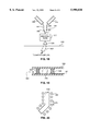
- FIGS. 4-17 A detailed description of preferred embodiments of the present invention is provided with reference to FIGS. 4-17, in which FIGS. 4 and 5 illustrate the basic concept.
- FIG. 4 shows the top view of a pair of orthogonal monopole antennas fabricated on a low cost printed circuit board according to the present invention.
- the dielectric layers are not shown for clarity. Rather, the three metalization layers are illustrated, including the first element 50 on the bottom surface of the device, the second element 51 on the top surface of the board, and the ground plane 53 disposed generally between the feed element 55 for the first element 50 and the feed element 54 for the second element 51.
- a first dielectric layer, not shown, is between the first element 50 and the ground plane 53
- a second dielectric, not shown is between the second element 51 and the ground plane 53
- a 50 ohm feed 54 is coupled to the second element 51 as shown in the figure.
- a 50 ohm feed 55 represented by the dashed lines, is coupled to the first element 50 on the bottom side.
- FIG. 5 shows a bottom view of the device, of FIG. 4.
- the first element 50 is found on the right side of the figure.
- the 50 ohm feed 55 overlays the ground plane 53.
- the second element 51 is found on the right side.
- the dielectric layers are not shown in FIG. 5.
- the monopole antennas such as the second element 51, comprise microstrips formed on the dielectric layer, which extend about ⁇ /4 beyond region generally 57 on the edge 58 of the ground plane 53, whereon ⁇ is the wavelength of the nominal center frequency for the communications device using the antenna.
- a 50 ohm feed which comprises an unbalanced microstrip extends from the antenna element 51, for connection to circuitry on the printed circuit board.
- the ground plane includes a triangular end region defined by the edge, generally 58.
- This triangular end region defined by the edge 58 includes a section 57 which is generally perpendicular to the second element 51 and a section 59 which is generally perpendicular to the first element 50.
- the impedance of the microstrip antenna elements 50 and 51, and the microstrip feed elements 54 and 55, is defined by the thickness of the dielectric, its dielectric constant, and the width of the line which defines the microstrip. This provides for matched impedance elements adapted for connection to standard transmission lines without matching circuits.
- the feed elements comprise 50 ohm matched feed lines, and the microstrip antennas are matched impedance microstrips for connection to the 50 ohm lines. This eliminates the need for matching networks on the printed circuit board.
- the ground plane 53 includes a generally triangular end section defined by the edge 58 and the regions 57 and 59. This shape is not necessarily triangular, however it is preferable that the regions 57 and 59 be generally orthogonal to one end of the respective antenna elements 50 and 51.
- perpendicular antennas isolated from one another by a combination of features is provided.
- the isolation is provided by using matched impedance feed lines, using the three layer circuit board structure and by the ground plane disposed generally between the antennas. Also, the isolation is enhanced by the orthogonal arrangement of the antennas.
- FIG. 6 illustrates an expanded view of a preferred embodiment of the present invention which has been designed to fit within the PCMCIA form factor for printed circuit boards.
- the edge of the printed circuit board is generally represented by the line 100.
- a first monopole element 101 is formed on the outside surface of a bottom layer of dielectric.
- a ground trace 102 is formed between the layers of the dielectric. Alternatively, the ground trace 102 could be placed on one or both of the outside surfaces of the dielectric and connected by vias to the ground plane.
- the ground plane 103 is formed in between the top and bottom layers of dielectric as described above with respect to FIGS. 4 and 5.
- a second monopole element 104 is formed on the outside surface of the top layer of the dielectric.
- a similar ground trace, not shown, is formed on the outside surface of the bottom layer of dielectric.
- the monopole element 104 is coupled to an unbalanced impedance matched feed line 106 which comprises a microstrip formed on the outside surface of the top layer of dielectric.
- a similar feed line generally 107 is formed connecting the element 101 to the circuitry, and formed on the outside surface of the bottom dielectric layer.
- Tuning stubs generally 108 and 109 are formed adjacent to the ends of the monopole elements 101 and 104, respectively.
- the monopole elements 101 and 104 are generally straight microstrips along the majority of their length, but have an elbow, 110, 111 near the end of the element to accommodate the form factor of the circuit board 100.
- a tip segment of the microstrip antenna generally 112 for element 101, and 113 for element 104, stand parallel to the sides, generally 114 and 115 of the printed circuit board 100. Because of the elbow structure, isolation of the antennas, due to the orthogonal relationship, is reduced. Thus, the ground trace 102 is added to improve that isolation.
- the ground plane 103 is coupled to the circuitry on the circuit board 100, by means of vias, generally 116. Also, a shield structure, not shown in FIG. 6, extends to a shield line 117.
- the shield comprises a conductive material which is coupled to the ground plane by means of the vias 116, shielding the circuitry on the circuit board 100 from the antenna structure.
- FIG. 7 illustrates a side view of the communications device assembly which includes the antenna structure of the present invention.
- a shield metal covering 120 is provided for a top side of the device, and a metal covering 121 is provided for the bottom side.
- Circuitry is mounted on the circuit board inside the shield structure.
- the ground vias 116 contact the shields 120 and 121 when the structure is assembled.
- the antenna system includes a first dielectric layer 125 and a second dielectric layer 126 which are coupled to the circuit board inside the shield, and extend beyond the shield.
- metalization 128 is provided to establish the ground trace 102 and the antenna element 104 of FIG. 6.
- the inside surface 129 of the first dielectric layer is coupled to the ground plane metalization 130.
- the inside surface 131 of the bottom layer 126 of dielectric is coupled to the ground plane 130.
- the outside surface 132 of the bottom layer of dielectric 126 carries metalization 133 for the antenna element 101 and a ground trace, not shown, in FIG. 6.
- the shield structure including metal 120 and plastic extension 140, and metal 121 and plastic extension 141 are snapped over the circuit board assembly and antenna system to enclosed the device.
- the plastic will be transparent to the RF wavelengths used by the communications device.
- FIG. 7 shows the tip of a printed circuit board, generally 139, which includes the antenna system of the present invention.
- An end view of the assembly of FIG. 7 is provided in FIG. 8.
- the shield member 120 and 121 are designed to connect with the three layer circuit board structure 139 at the positions of the vias 116, shown in FIGS. 6 and 7.
- layers 2-5 of a 6-layer printed circuit board PCB are fused to create, ineffect, 3 layers. Cut out regions 150 for the top layer and 151 for the bottom layer on the shield structure 120 and 121 provide for passage of the unbalanced feed lines 106 and 107 inside the shield from the antenna structure outside.
- a buried signal line can be used as described below with respect to FIGS. 18 through 20.
- FIGS. 9 and 10 illustrate variations in the layout of the dual monopole antenna system of the present invention to illustrate certain optional features.
- FIG. 9 illustrates a layout which includes monopole elements 160 and 161 arranged generally orthogonally to one another. These monopole elements include the elbows, generally 162 and 163, and tuning stubs, generally 164 and 165, shown in FIG. 6. However, no ground trace 102 is utilized in this embodiment.
- FIG. 10 illustrates yet an alternative approach.
- a first monopole antenna 170 including an elbow 171 is provided.
- a second monopole antenna 172 including elbow 173 is arranged generally orthogonally to the first monopole antenna 170.
- a ground plane 174 having the characteristics described above with reference to FIGS. 4 and 5 is included.
- tuning stubs generally 175 and 176 used near the ends of the monopole elements 170 and 172, such that the effective length of the monopole elements can be tuned as needed.
- a ground trace 177 is included on the outside surfaces of the dielectric layers.
- vias, generally 178, are included in the ground traces which couple the ground traces on the top and bottom together.
- a plurality of tuning stubs 179 is used in association with the ground traces 177 for optimizing performance of the system.
- tuning stubs 180 and tuning stubs 181 for use in connection with the ground plane 174 are added.
- FIGS. 11-17 illustrate the circuitry used for selecting an active one or a combination of active antennas for the communications device.
- FIG. 11 a conceptual schematic diagram of one approach to selecting an active antenna is illustrated.
- a first antenna 210 and a second antenna 211 are provided.
- Each antenna is coupled to a switch S1 and S2, respectively.
- the switches are coupled to a summing junction 212.
- the output of the summing junction is provided on line 213 to the rest of the communications device or transceiver.
- a switch driver 214 controls the switches S1 and S2, so that the active antenna can be changed to take optimum advantage of spatial diversity for the device.
- an intelligent switch driver actively determines the antenna receiving the best signal, and selects that antenna as the active device.
- the intelligent switch driver may comprise software in the processor driving the transceiver which uses the antennas that executes an algorithm to improve antenna performance using so-called selection diversity. According to selection diversity, the dynamic algorithm determines which antenna is receiving the signal best, and controls the switch to optimize the use of the antenna diversity.
- the switch driver 212 automatically switches between antennas independent of other processing.
- This automatic dithering between antennas is suitable for low-cost, low traffic uses.
- the timing wave forms, according to this low frequency dithering aspect of the present invention can take the shapes shown in FIGS. 12 and 13.
- FIG. 12 a four state antenna system is provided.
- the oscillating driver 214 periodically switches the antenna system through the four states automatically.
- one period for the oscillating switch driver 214 is a 100 millisecond cycle, generally 220.
- cycle 220 there is a first state, generally 221, in which both switches are on, a second state, generally 222, during which switch S1 is on and switch S2 is off, a third state, generally 223, during which both switches are on, and a fourth state, generally 224, during which switch S2 is on and switch S1 is off.
- This cycle 220 continuously and automatically repeats to ensure spatial diversity in the receiving system.
- transition T the transitions, such as transition T, are relatively gradual, so that the switches turn off slowly.
- the transition time T is substantially greater than the characteristic packet reception time of the system.
- the maximum packet length is about 1.22 milliseconds.
- the transition time T for such a system would range from 2 to 10 milliseconds.
- the gradual transition T allows for a "fade" effect as the state changes, so that packets being transmitted or received during the change are less likely to be lost.
- the cycle time 220 is on the order of 100 milliseconds or less, so that within the human reaction time, the best state of the antenna system will be provided for communicating a given packet. Thus, if the packet transmitted during a state during which poor reception occurs, it will be retried during a following state, within a period of time which is not noticeable by human operators.
- each of the states is substantially longer than the maximum packet length in the communication system. This ensures that during any given state, a number of packets can be transmitted successfully before a less desirable antenna configuration is switched to.
- the period of oscillating switch driver is substantially greater than the maximum packet length, preferably each state during the period 220 is greater than 10 times the maximum packet length.
- the four state cycle 220 offers in effect three antenna configurations to combat multipath effects with spatial diversity.
- a "array antenna” is set up which has spatial characteristics which appear offset to region between the two antennas.
- each cycle generally 230, has two states, state 231, during which switch S1 is on, and state 232, during which S2 is on.
- the cycle time is on the order of 100 milliseconds or less.
- the packet length is much shorter than the dwell time on each antenna position. For example, if the period of the digital oscillator is equal to 100 milliseconds and the packet length is only 1.2 milliseconds, as in the case of Ethernet, many packets can be transmitted during each antenna configuration state. If both states are such that neither antenna is in a multipath null, then no packets are dropped. If one antenna position is in a null, then the probability of the other position being in a null is vanishingly small. The period of less than about 100 milliseconds. If one position is in a null, there will be an interruption in the link, but the user will not perceive the delay due to the fact that one tenth of a second is very short in terms of human reaction times. In addition, the switching on and off is done relatively gradually. This is done so that the receiver sees no switching impulses, and so that the antenna environment changes gradually with respect to packet length.
- FIG. 14 illustrates a monolithic microwave integrated circuit design, which could be used for the switches S1 and S2 in an integrated circuit embodiment of the present invention.
- the switch is based on three MESFET transistors, Q1, Q2, and Q3.
- the oscillating switch driver supplies a control signal on line 250, having a shape, such as illustrated for switch S1 or switch S2 in FIG. 12 or FIG. 13.
- the control signal is supplied through buffer 251 to the gate of transistor Q1 across line 252.
- the output of the buffer 251 is connected to an inverter 253.
- the output of the inverter 253 is connected across line 254 to the gates of transistors Q2 and Q3.
- the drain of transistor Q1 is connected to PORT1 which would be connected to the feed for an antenna, such as antenna 210 of FIG. 11.
- the source of transistor Q1 is connected to PORT2, which is connected to the summing junction 212 of the circuit of FIG. 11.
- the drain of transistor Q2 is connected to PORT2, and the emitter of transistor Q2 is connected through a capacitor 255 to ground.
- the drain of transistor Q3 is connected to PORT1, and the emitter of transistor Q3 is connected to a capacitor 256 to ground.
- Each of the transistors Q1, Q2, and Q3 has a resistor, R1, R2, R3 connected across its source and drain, and a resistor R4, R5, R6 connected from the source to a bias potential VBIAS.
- the voltage VBIAS is essentially one diode drop below the power supply level V DD for the circuit.
- FIG. 15 is a timing diagram for operation of the switch of FIG. 14.
- the control signal is shown at trace 260
- the output of the buffer 251 is shown at trace 261
- the output of the inverter 253 is shown at trace 262.
- the switch provides a gradual switching from a first open state to a closed state, determined by the slope of the transition, generally 263, on the control signal 260.
- transistor Q1 slowly turns on, directly connecting PORT1 to PORT2.
- transistors Q3 and Q4 slowly turn off in response to the output of the inverter, disconnecting PORT1 and PORT2 from ground.
- the transistor Q1 turns off as the control signal drops, while transistors Q3 and Q2 turn on.
- FIG. 16 illustrates a preferred embodiment of the summing junction 212 of FIG. 11.
- a Wilkinson coupler is utilized to connect the outputs of the switches to a single ended unbalanced line to the circuitry of the communications device.
- the output of switch S1 is supplied on line 270 to a 50 ohm microstrip 271.
- the 50 ohm microstrip 271 is coupled to a 70 ohm microstrip 272 which is about ⁇ /4 long, where ⁇ is the wavelength of the nominal center frequency of the communications device.
- the 70 ohm microstrip 272 is coupled to a 50 ohm microstrip 273 which provides the output on line 274.
- the input from the second switch is provided on line 275 to a 50 ohm microstrip 276.
- the 50 ohm microstrip 276 is connected to a 70 ohm microstrip 277 which is about ⁇ /4 long, which is in turn coupled to the rnicrostrip 273.
- a resistor 278 is coupled between the ends of the microstrips 271 and 276 adjacent the connections to the 70 ohm microstrips 272 and 277. This is a 100 ohm resistor in the embodiment illustrated, used for isolation of the two inputs.
- FIG. 17 An alternative system can be implemented using a monolithic microwave integrated circuit switch as shown in FIG. 17.
- This switch is useful, for instance, when the antennas are controlled so that one is on or the other is selected, and never both at the same time. Furthermore, this switch would be useful if the switching between antennas is controlled by the host processor in response to the quality of the signals received on the antennas, rather than automatically as described above with reference to FIGS. 12-13.
- FIG. 17 is a switch based on four MESFET transistors Q10, Q11, Q12, and Q13.
- the antennas are connected to PORT1 and PORT2, respectively.
- the output of the switching circuit is applied to the common node 284.
- a control signal is received on line 280 and supplied to buffer 281.
- the output of the buffer is applied on line 282 to the gates of transistors Q10 and Q12.
- the output of the buffer is applied to inverter 283.
- the output of the inverter 283 is applied to the gates of transistors Q11 and Q13.
- Transistor Q10 has its drain connected to PORT1, and its source connected to the common node 284.
- Transistor Q11 has its drain connected to PORT2 and its source connected to the common node 284.
- Transistor Q13 has its drain connected to PORT1 and its source connected through capacitor 285 to ground.
- Transistor Q12 has its drain connected to PORT2 and its source connected across capacitor 286 to around.
- Each ofthe transistors Q10-Q13 has a resistor R10, R11, R12, and R13 connected across its drain and source.
- the common node 284 is connected across resistor R14 to the potential VBIAS which is about one diode drop below the supply voltage V DD .
- the drains of transistors Q12 and Q13 are coupled across transistors R15 and R16, respectively to the bias potential VBIAS. In operation, when the control signal on line 280 is high, transistors Q10 and Q12 are on.
- transistors Q11 and Q13 are on, connecting PORT2 to the common node 284, and pulling PORT1 to AC ground.
- the common node 284 is connected to the circuitry of the communication device directly, so no summing junction, such as that illustrated in FIG. 16, is required.
- the two antennas of the system are connected to a summing junction through a pair of switches.
- the switches can be intelligently controlled or controlled by a free running, oscillating digital logic circuit which produces the waveform shown in FIGS. 12 or 13.
- FIGS. 18 through 20 show an alternative embodiment for positioning the dual orthogonal antennas outside of the shield structure in a printed circuit board embodiment like that shown in FIG. 7.
- a signal line 309 is buried between the layers of dielectric (125 and 126 of FIG. 7) and connected to the circuits inside the shield structure. Therefore, no notches (150-151 in FIG. 8) are necessary in the shield structure.
- first and second orthogonal microstrip antennas 300 and 301 are formed on the outside surfaces of the dielectric as discussed above.
- the ground plane and other structures for the orthogonal monopoles are not shown in FIG. 18 for simplicity.
- the antennas are intended to have the structure discussed above, for instance with reference to FIG. 6.
- the first antenna 300 has feed line 302 which is connected to a first pole 303 of switch 304.
- the second antenna 301 has a feed line 305 connected to the second pole 306 of the switch 304.
- the switch supplies the selected signal through a bandpass filter 307 to a signal line via 308 on the surface of the board.
- the signal line via 308 connects to the signal line represented by the dotted lines 309, which is formed in the metalization between the layers of dielectric.
- the shield barrier is illustrated by the line 310 in FIG. 18.
- the signal line 309 provides a means for providing a signal from node 308 into the circuitry within the shield.
- the switch 304 can be implemented using a very small monolithic microwave integrated circuit (MMIC) with techniques known in the art.
- MMIC monolithic microwave integrated circuit
- the filter 307 can also be a small surface mounted device. This structure can be mounted on the outside surface of one of the dielectric layers.
- FIG. 19 shows the buried signal line 309 in the dielectric structure.
- a top ground plane 320 and a bottom ground plane 321 are shown.
- the dielectric layers are formed generally in the region 322.
- Vias 323 and 324 are formed along the sides of the signal line 309.
- the height and width of the signal line 309 are adjusted to establish a 50 ohm strip line for a short run.
- the strip line is centered within the structure to improve the impedance characteristics.
- the signal line 309 is laid out in top view as shown in FIG. 20.
- the signal line 309 has vias generally 330 arrayed along the side of the signal line in a "picket fence" arrangement. The space in between the vias is about one tenth of the wavelength of the center frequency to shield the buried strip line.
- a preferred system may provide for a buried signal line which reduces the manufacturing costs of the shielding structures for the system according to the present invention, with an antenna switch MMIC and bandpass filter placed outside the shield.
- an improved antenna system for a communications device allows for low cost manufacture while maintaining spatial diversity on a small device, such as within the PCMCIA form factor.
- the antenna system is based on orthogonally disposed isolated monopoles fabricated on multilayer printed circuit board. Tests of the return loss of elements configured as shown in FIG. 6 illustrate a very good return loss and isolation between the antennas over frequency. The return loss has been measured at below 15 dB for an untuned trace, and below 27 dB for a tuned trace across the 2.4 to 2.485 GHz ISM band. This implies an excellent 50 ohm match with a very low loss feed. Furthermore, isolation is better than 15 dB for both the top and bottom traces, implying little interaction between each element. The bandwidth for both antennas is much wider than the ISM band itself Thus, normal manufacturing tolerances will have little effect on antenna performance.
- an efficient antenna system which is physically small and can be fabricated on a low cost printed circuit board.
- the bandwidth is wide enough to account for manufacturing tolerances without degrading performance.
- the system includes impedance matched elements, so that no matching circuits are required; and provides a 50 ohm unbalanced line feed for each antenna simplifying connection to the circuitry which relies on the antennas.
- each antenna is electrically isolated from the other, so that true spatial diversity can be achieved.
Abstract
Description
Claims (45)
Priority Applications (1)
| Application Number | Priority Date | Filing Date | Title |
|---|---|---|---|
| US08/660,964 US5990838A (en) | 1996-06-12 | 1996-06-12 | Dual orthogonal monopole antenna system |
Applications Claiming Priority (1)
| Application Number | Priority Date | Filing Date | Title |
|---|---|---|---|
| US08/660,964 US5990838A (en) | 1996-06-12 | 1996-06-12 | Dual orthogonal monopole antenna system |
Publications (1)
| Publication Number | Publication Date |
|---|---|
| US5990838A true US5990838A (en) | 1999-11-23 |
Family
ID=24651640
Family Applications (1)
| Application Number | Title | Priority Date | Filing Date |
|---|---|---|---|
| US08/660,964 Expired - Lifetime US5990838A (en) | 1996-06-12 | 1996-06-12 | Dual orthogonal monopole antenna system |
Country Status (1)
| Country | Link |
|---|---|
| US (1) | US5990838A (en) |
Cited By (152)
| Publication number | Priority date | Publication date | Assignee | Title |
|---|---|---|---|---|
| US6107970A (en) * | 1998-10-07 | 2000-08-22 | Ericsson Inc. | Integral antenna assembly and housing for electronic device |
| US6222503B1 (en) * | 1997-01-10 | 2001-04-24 | William Gietema | System and method of integrating and concealing antennas, antenna subsystems and communications subsystems |
| US6295462B1 (en) * | 1997-12-19 | 2001-09-25 | Nec Corporation | Portable radio information terminal |
| WO2001078192A2 (en) * | 2000-04-05 | 2001-10-18 | Research In Motion Limited | Multi-feed antenna sytem |
| US6433742B1 (en) | 2000-10-19 | 2002-08-13 | Magis Networks, Inc. | Diversity antenna structure for wireless communications |
| US6456245B1 (en) | 2000-12-13 | 2002-09-24 | Magis Networks, Inc. | Card-based diversity antenna structure for wireless communications |
| US6456242B1 (en) | 2001-03-05 | 2002-09-24 | Magis Networks, Inc. | Conformal box antenna |
| US20020140615A1 (en) * | 1999-09-20 | 2002-10-03 | Carles Puente Baliarda | Multilevel antennae |
| US6549170B1 (en) | 2002-01-16 | 2003-04-15 | Accton Technology Corporation | Integrated dual-polarized printed monopole antenna |
| US20030112190A1 (en) * | 2000-04-19 | 2003-06-19 | Baliarda Carles Puente | Advanced multilevel antenna for motor vehicles |
| US6624790B1 (en) | 2002-05-08 | 2003-09-23 | Accton Technology Corporation | Integrated dual-band printed monopole antenna |
| US20030210199A1 (en) * | 2000-09-08 | 2003-11-13 | 3Com Corporation | Extendable planar diversity antenna |
| US6664930B2 (en) | 2001-04-12 | 2003-12-16 | Research In Motion Limited | Multiple-element antenna |
| US20040036655A1 (en) * | 2002-08-22 | 2004-02-26 | Robert Sainati | Multi-layer antenna structure |
| US20040051669A1 (en) * | 2000-07-10 | 2004-03-18 | Tomas Rutfors | Antenna arrangement and a portable radio communication device |
| US6725057B1 (en) * | 1999-05-10 | 2004-04-20 | Koninklijke Philips Electronics N.V. | Personal communications apparatus |
| US20040075613A1 (en) * | 2002-06-21 | 2004-04-22 | Perry Jarmuszewski | Multiple-element antenna with parasitic coupler |
| US6791500B2 (en) | 2002-12-12 | 2004-09-14 | Research In Motion Limited | Antenna with near-field radiation control |
| US20040183726A1 (en) * | 2003-03-18 | 2004-09-23 | Theobold David M. | Multichannel access point with collocated isolated antennas |
| US20040192226A1 (en) * | 2003-03-31 | 2004-09-30 | Motorola, Inc. | Miniature vertically polarized multiple frequency band antenna and method of providing an antenna for a wireless device |
| US6812897B2 (en) | 2002-12-17 | 2004-11-02 | Research In Motion Limited | Dual mode antenna system for radio transceiver |
| US20040227680A1 (en) * | 2003-05-14 | 2004-11-18 | Geyi Wen | Antenna with multiple-band patch and slot structures |
| WO2004105182A1 (en) * | 2003-05-19 | 2004-12-02 | Antenova Limited | Dual band antenna system with diversity |
| US20050001769A1 (en) * | 2003-06-12 | 2005-01-06 | Yihong Qi | Multiple-element antenna with floating antenna element |
| US20050017906A1 (en) * | 2003-07-24 | 2005-01-27 | Man Ying Tong | Floating conductor pad for antenna performance stabilization and noise reduction |
| US6870507B2 (en) | 2001-02-07 | 2005-03-22 | Fractus S.A. | Miniature broadband ring-like microstrip patch antenna |
| US6876320B2 (en) | 2001-11-30 | 2005-04-05 | Fractus, S.A. | Anti-radar space-filling and/or multilevel chaff dispersers |
| US20050078042A1 (en) * | 2003-09-22 | 2005-04-14 | Thales Plc | Antenna |
| US20050116869A1 (en) * | 2003-10-28 | 2005-06-02 | Siegler Michael J. | Multi-band antenna structure |
| US20050128162A1 (en) * | 2003-12-10 | 2005-06-16 | Matsushita Electric Industrail Co., Ltd. | Antenna |
| US20050140551A1 (en) * | 2003-12-30 | 2005-06-30 | Heiko Kaluzni | High performance low cost monopole antenna for wireless applications |
| US20050184922A1 (en) * | 2004-02-24 | 2005-08-25 | Fujitsu Limited | Control device for antenna matching circuit |
| US6937191B2 (en) | 1999-10-26 | 2005-08-30 | Fractus, S.A. | Interlaced multiband antenna arrays |
| US6937206B2 (en) | 2001-04-16 | 2005-08-30 | Fractus, S.A. | Dual-band dual-polarized antenna array |
| US20050195124A1 (en) * | 2002-09-10 | 2005-09-08 | Carles Puente Baliarda | Coupled multiband antennas |
| JP2005347958A (en) * | 2004-06-01 | 2005-12-15 | Toshiba Corp | Antenna device |
| US20060044193A1 (en) * | 2003-06-09 | 2006-03-02 | Susumu Fukushima | Antenna and electronic device using the same |
| US20060050000A1 (en) * | 2003-12-19 | 2006-03-09 | Sony Corporation | Antenna device, radio device, and electronic instrument |
| US7071879B2 (en) | 2004-06-01 | 2006-07-04 | Ems Technologies Canada, Ltd. | Dielectric-resonator array antenna system |
| US7148850B2 (en) | 2000-01-19 | 2006-12-12 | Fractus, S.A. | Space-filling miniature antennas |
| EP1744262A3 (en) * | 2003-11-13 | 2007-03-28 | Hospira, Inc. | System for maintaining drug information and communicating with medication delivery devices |
| US7202818B2 (en) | 2001-10-16 | 2007-04-10 | Fractus, S.A. | Multifrequency microstrip patch antenna with parasitic coupled elements |
| US7215287B2 (en) | 2001-10-16 | 2007-05-08 | Fractus S.A. | Multiband antenna |
| US20070152894A1 (en) * | 2002-12-22 | 2007-07-05 | Fractus, S.A. | Multi-band monopole antenna for a mobile communications device |
| US7245196B1 (en) | 2000-01-19 | 2007-07-17 | Fractus, S.A. | Fractal and space-filling transmission lines, resonators, filters and passive network elements |
| US20070213598A1 (en) * | 2003-11-13 | 2007-09-13 | Howard Gary A | System for maintaining drug information and communicating with medication delivery devices |
| US20070233049A1 (en) * | 2006-03-28 | 2007-10-04 | Hospira, Inc. | Medication administration and management system and method |
| US20070247255A1 (en) * | 2004-08-18 | 2007-10-25 | Victor Shtrom | Reducing stray capacitance in antenna element switching |
| US20070257846A1 (en) * | 2004-05-13 | 2007-11-08 | Geyi Wen | Antenna with multiple-band patch and slot structures |
| US20070285317A1 (en) * | 2006-06-13 | 2007-12-13 | Compal Electronics, Inc. | Modulized antenna structure |
| US7312762B2 (en) | 2001-10-16 | 2007-12-25 | Fractus, S.A. | Loaded antenna |
| JP2008503941A (en) * | 2004-06-17 | 2008-02-07 | インターデイジタル テクノロジー コーポレーション | Low profile smart antenna for wireless applications and related methods |
| US20080139136A1 (en) * | 2005-06-24 | 2008-06-12 | Victor Shtrom | Multiple-Input Multiple-Output Wireless Antennas |
| US20080200870A1 (en) * | 2005-04-11 | 2008-08-21 | Hospira, Inc. | System for guiding a user during programming of a medical device |
| US20080198082A1 (en) * | 2005-05-13 | 2008-08-21 | Fractus, S.A. | Antenna Diversity System and Slot Antenna Component |
| US7417588B2 (en) | 2004-01-30 | 2008-08-26 | Fractus, S.A. | Multi-band monopole antennas for mobile network communications devices |
| US20080204331A1 (en) * | 2007-01-08 | 2008-08-28 | Victor Shtrom | Pattern Shaping of RF Emission Patterns |
| US7423592B2 (en) | 2004-01-30 | 2008-09-09 | Fractus, S.A. | Multi-band monopole antennas for mobile communications devices |
| WO2007127087A3 (en) * | 2006-04-28 | 2008-10-16 | Ruckus Wireless Inc | Multiband omnidirectional planar antenna apparatus with selectable elements |
| US20080266199A1 (en) * | 2005-10-14 | 2008-10-30 | Zlatoljub Milosavljevic | Adjustable antenna and methods |
| US7498999B2 (en) | 2004-11-22 | 2009-03-03 | Ruckus Wireless, Inc. | Circuit board having a peripheral antenna apparatus with selectable antenna elements and selectable phase shifting |
| US7498996B2 (en) | 2004-08-18 | 2009-03-03 | Ruckus Wireless, Inc. | Antennas with polarization diversity |
| WO2009030038A1 (en) * | 2007-09-04 | 2009-03-12 | Sierra Wireless, Inc. | Antenna configurations for compact device wireless communication |
| US7511680B2 (en) | 2004-08-18 | 2009-03-31 | Ruckus Wireless, Inc. | Minimized antenna apparatus with selectable elements |
| US7511675B2 (en) | 2000-10-26 | 2009-03-31 | Advanced Automotive Antennas, S.L. | Antenna system for a motor vehicle |
| US7525486B2 (en) | 2004-11-22 | 2009-04-28 | Ruckus Wireless, Inc. | Increased wireless coverage patterns |
| US20090115670A1 (en) * | 2007-09-04 | 2009-05-07 | Sierra Wireless, Inc. | Antenna Configurations for Compact Device Wireless Communication |
| US20090121948A1 (en) * | 2007-09-04 | 2009-05-14 | Sierra Wireless, Inc. | Antenna Configurations for Compact Device Wireless Communication |
| US20090122847A1 (en) * | 2007-09-04 | 2009-05-14 | Sierra Wireless, Inc. | Antenna Configurations for Compact Device Wireless Communication |
| US20090124215A1 (en) * | 2007-09-04 | 2009-05-14 | Sierra Wireless, Inc. | Antenna Configurations for Compact Device Wireless Communication |
| US20090262028A1 (en) * | 2005-07-21 | 2009-10-22 | Josep Mumbru | Handheld device with two antennas, and method of enhancing the isolation between the antennas |
| US7639106B2 (en) | 2006-04-28 | 2009-12-29 | Ruckus Wireless, Inc. | PIN diode network for multiband RF coupling |
| EP1988600A3 (en) * | 2007-04-30 | 2010-03-03 | Telefonaktiebolaget LM Ericsson (publ) | Antenna with a pivotally adjustable structure |
| US20100087224A1 (en) * | 2008-10-02 | 2010-04-08 | Samsung Electronics Co., Ltd. | Multi-standby portable terminal |
| US20100245191A1 (en) * | 2006-05-30 | 2010-09-30 | Broadcom Corporation | Multiple mode rf transceiver and antenna structure |
| US20100265141A1 (en) * | 2008-04-21 | 2010-10-21 | Ralink Technology Corporation | Antenna and wireless transceiver using the same |
| US7880683B2 (en) | 2004-08-18 | 2011-02-01 | Ruckus Wireless, Inc. | Antennas with polarization diversity |
| US7965252B2 (en) | 2004-08-18 | 2011-06-21 | Ruckus Wireless, Inc. | Dual polarization antenna array with increased wireless coverage |
| US8031129B2 (en) | 2004-08-18 | 2011-10-04 | Ruckus Wireless, Inc. | Dual band dual polarization antenna array |
| US8049671B2 (en) | 2007-09-04 | 2011-11-01 | Sierra Wireless, Inc. | Antenna configurations for compact device wireless communication |
| US8068068B2 (en) | 2005-06-24 | 2011-11-29 | Ruckus Wireless, Inc. | Coverage antenna apparatus with selectable horizontal and vertical polarization elements |
| US20120169560A1 (en) * | 2009-10-30 | 2012-07-05 | Laird Technologies, Inc. | Omnidirectional multi-band antennas |
| US8217843B2 (en) | 2009-03-13 | 2012-07-10 | Ruckus Wireless, Inc. | Adjustment of radiation patterns utilizing a position sensor |
| US20120206301A1 (en) * | 2009-09-24 | 2012-08-16 | Taoglas Group Holdings | Multi-angle ultra wideband antenna with surface mount technology methods of assembly and kits therefor |
| US20130207877A1 (en) * | 2012-02-14 | 2013-08-15 | Victor Shtrom | Radio frequency antenna array with spacing element |
| US20140078018A1 (en) * | 2012-09-14 | 2014-03-20 | Acer Incorporated | Communication device and antenna system with high isolation |
| US8698675B2 (en) | 2009-05-12 | 2014-04-15 | Ruckus Wireless, Inc. | Mountable antenna elements for dual band antenna |
| US8738103B2 (en) | 2006-07-18 | 2014-05-27 | Fractus, S.A. | Multiple-body-configuration multimedia and smartphone multifunction wireless devices |
| US8756668B2 (en) | 2012-02-09 | 2014-06-17 | Ruckus Wireless, Inc. | Dynamic PSK for hotspots |
| TWI449258B (en) * | 2010-10-05 | 2014-08-11 | Univ Nat Sun Yat Sen | Mimo mobile communication device |
| US20140225800A1 (en) * | 2013-02-12 | 2014-08-14 | Qualcomm Incorporated | Apparatus and methods to improve antenna isolation |
| US8854273B2 (en) | 2011-06-28 | 2014-10-07 | Industrial Technology Research Institute | Antenna and communication device thereof |
| US9019165B2 (en) | 2004-08-18 | 2015-04-28 | Ruckus Wireless, Inc. | Antenna with selectable elements for use in wireless communications |
| US9077084B2 (en) | 2012-04-03 | 2015-07-07 | Industrial Technology Research Institute | Multi-band multi-antenna system and communication device thereof |
| US9092610B2 (en) | 2012-04-04 | 2015-07-28 | Ruckus Wireless, Inc. | Key assignment for a brand |
| CN104852129A (en) * | 2014-02-19 | 2015-08-19 | 日本安特尼株式会社 | Antenna device |
| US9407012B2 (en) | 2010-09-21 | 2016-08-02 | Ruckus Wireless, Inc. | Antenna with dual polarization and mountable antenna elements |
| US9570799B2 (en) | 2012-09-07 | 2017-02-14 | Ruckus Wireless, Inc. | Multiband monopole antenna apparatus with ground plane aperture |
| US9634403B2 (en) | 2012-02-14 | 2017-04-25 | Ruckus Wireless, Inc. | Radio frequency emission pattern shaping |
| US9755314B2 (en) | 2001-10-16 | 2017-09-05 | Fractus S.A. | Loaded antenna |
| US9960478B2 (en) | 2014-07-24 | 2018-05-01 | Fractus Antennas, S.L. | Slim booster bars for electronic devices |
| US9971871B2 (en) | 2011-10-21 | 2018-05-15 | Icu Medical, Inc. | Medical device update system |
| US10022498B2 (en) | 2011-12-16 | 2018-07-17 | Icu Medical, Inc. | System for monitoring and delivering medication to a patient and method of using the same to minimize the risks associated with automated therapy |
| US10042986B2 (en) | 2013-11-19 | 2018-08-07 | Icu Medical, Inc. | Infusion pump automation system and method |
| US10103449B2 (en) | 2015-12-08 | 2018-10-16 | Industrial Technology Research Institute | Antenna array |
| US10166328B2 (en) | 2013-05-29 | 2019-01-01 | Icu Medical, Inc. | Infusion system which utilizes one or more sensors and additional information to make an air determination regarding the infusion system |
| US10230161B2 (en) | 2013-03-15 | 2019-03-12 | Arris Enterprises Llc | Low-band reflector for dual band directional antenna |
| US10238801B2 (en) | 2009-04-17 | 2019-03-26 | Icu Medical, Inc. | System and method for configuring a rule set for medical event management and responses |
| US10238799B2 (en) | 2014-09-15 | 2019-03-26 | Icu Medical, Inc. | Matching delayed infusion auto-programs with manually entered infusion programs |
| US10242060B2 (en) | 2006-10-16 | 2019-03-26 | Icu Medical, Inc. | System and method for comparing and utilizing activity information and configuration information from multiple medical device management systems |
| US10263336B1 (en) | 2017-12-08 | 2019-04-16 | Industrial Technology Research Institute | Multi-band multi-antenna array |
| DE102018128238A1 (en) | 2017-11-14 | 2019-05-16 | Ford Global Technologies, Llc | DETECTION SYSTEM OF MOBILE DEVICES IN A VEHICLE CABIN |
| US10311972B2 (en) | 2013-11-11 | 2019-06-04 | Icu Medical, Inc. | Medical device system performance index |
| US10314974B2 (en) | 2014-06-16 | 2019-06-11 | Icu Medical, Inc. | System for monitoring and delivering medication to a patient and method of using the same to minimize the risks associated with automated therapy |
| US10333213B2 (en) | 2016-12-06 | 2019-06-25 | Silicon Laboratories Inc. | Apparatus with improved antenna isolation and associated methods |
| US10333843B2 (en) | 2013-03-06 | 2019-06-25 | Icu Medical, Inc. | Medical device communication method |
| US10342917B2 (en) | 2014-02-28 | 2019-07-09 | Icu Medical, Inc. | Infusion system and method which utilizes dual wavelength optical air-in-line detection |
| US10367266B2 (en) | 2016-12-27 | 2019-07-30 | Industrial Technology Research Institute | Multi-antenna communication device |
| US10430761B2 (en) | 2011-08-19 | 2019-10-01 | Icu Medical, Inc. | Systems and methods for a graphical interface including a graphical representation of medical data |
| US10434246B2 (en) | 2003-10-07 | 2019-10-08 | Icu Medical, Inc. | Medication management system |
| US10469589B2 (en) | 2017-11-14 | 2019-11-05 | Ford Global Technologies, Llc | Vehicle cabin mobile device sensor system |
| US10463788B2 (en) | 2012-07-31 | 2019-11-05 | Icu Medical, Inc. | Patient care system for critical medications |
| US10578474B2 (en) | 2012-03-30 | 2020-03-03 | Icu Medical, Inc. | Air detection system and method for detecting air in a pump of an infusion system |
| US10596316B2 (en) | 2013-05-29 | 2020-03-24 | Icu Medical, Inc. | Infusion system and method of use which prevents over-saturation of an analog-to-digital converter |
| US10635784B2 (en) | 2007-12-18 | 2020-04-28 | Icu Medical, Inc. | User interface improvements for medical devices |
| US10656894B2 (en) | 2017-12-27 | 2020-05-19 | Icu Medical, Inc. | Synchronized display of screen content on networked devices |
| US10692595B2 (en) | 2018-07-26 | 2020-06-23 | Icu Medical, Inc. | Drug library dynamic version management |
| US10741280B2 (en) | 2018-07-17 | 2020-08-11 | Icu Medical, Inc. | Tagging pump messages with identifiers that facilitate restructuring |
| US10765799B2 (en) | 2013-09-20 | 2020-09-08 | Icu Medical, Inc. | Fail-safe drug infusion therapy system |
| US10784593B1 (en) * | 2018-08-02 | 2020-09-22 | United States Of America As Represented By The Administrator Of The National Aeronautics And Space Administration | Dual-band and wideband patch antenna |
| US10850024B2 (en) | 2015-03-02 | 2020-12-01 | Icu Medical, Inc. | Infusion system, device, and method having advanced infusion features |
| US10861592B2 (en) | 2018-07-17 | 2020-12-08 | Icu Medical, Inc. | Reducing infusion pump network congestion by staggering updates |
| US10873349B1 (en) * | 2019-06-20 | 2020-12-22 | Motorola Solutions, Inc. | Portable communication device with antenna radiation pattern control |
| US10874793B2 (en) | 2013-05-24 | 2020-12-29 | Icu Medical, Inc. | Multi-sensor infusion system for detecting air or an occlusion in the infusion system |
| US10898641B2 (en) | 2014-04-30 | 2021-01-26 | Icu Medical, Inc. | Patient care system with conditional alarm forwarding |
| US11135360B1 (en) | 2020-12-07 | 2021-10-05 | Icu Medical, Inc. | Concurrent infusion with common line auto flush |
| CN113875088A (en) * | 2019-03-18 | 2021-12-31 | 弗雷德里克·奈卜克 | Ultra-wideband (UWB) link configuration method and system |
| US11246985B2 (en) | 2016-05-13 | 2022-02-15 | Icu Medical, Inc. | Infusion pump system and method with common line auto flush |
| US11276942B2 (en) | 2019-12-27 | 2022-03-15 | Industrial Technology Research Institute | Highly-integrated multi-antenna array |
| US11278671B2 (en) | 2019-12-04 | 2022-03-22 | Icu Medical, Inc. | Infusion pump with safety sequence keypad |
| US11309070B2 (en) | 2018-07-26 | 2022-04-19 | Icu Medical, Inc. | Drug library manager with customized worksheets |
| US11328805B2 (en) | 2018-07-17 | 2022-05-10 | Icu Medical, Inc. | Reducing infusion pump network congestion by staggering updates |
| US11324888B2 (en) | 2016-06-10 | 2022-05-10 | Icu Medical, Inc. | Acoustic flow sensor for continuous medication flow measurements and feedback control of infusion |
| US11344673B2 (en) | 2014-05-29 | 2022-05-31 | Icu Medical, Inc. | Infusion system and pump with configurable closed loop delivery rate catch-up |
| US11344668B2 (en) | 2014-12-19 | 2022-05-31 | Icu Medical, Inc. | Infusion system with concurrent TPN/insulin infusion |
| US11571508B2 (en) | 2013-08-30 | 2023-02-07 | Icu Medical, Inc. | System and method of monitoring and managing a remote infusion regimen |
| US11574737B2 (en) | 2016-07-14 | 2023-02-07 | Icu Medical, Inc. | Multi-communication path selection and security system for a medical device |
| US11587669B2 (en) | 2018-07-17 | 2023-02-21 | Icu Medical, Inc. | Passing authentication token to authorize access to rest calls via web sockets |
| US11605468B2 (en) | 2015-05-26 | 2023-03-14 | Icu Medical, Inc. | Infusion pump system and method with multiple drug library editor source capability |
| US11664595B1 (en) | 2021-12-15 | 2023-05-30 | Industrial Technology Research Institute | Integrated wideband antenna |
| US11862868B2 (en) | 2021-12-20 | 2024-01-02 | Industrial Technology Research Institute | Multi-feed antenna |
| US11883361B2 (en) | 2020-07-21 | 2024-01-30 | Icu Medical, Inc. | Fluid transfer devices and methods of use |
Citations (18)
| Publication number | Priority date | Publication date | Assignee | Title |
|---|---|---|---|---|
| US3798548A (en) * | 1971-09-08 | 1974-03-19 | Ameco Inc | Discrete cable television distribution system |
| US3803617A (en) * | 1972-04-14 | 1974-04-09 | Nasa | High efficiency multifrequency feed |
| US4072951A (en) * | 1976-11-10 | 1978-02-07 | The United States Of America As Represented By The Secretary Of The Navy | Notch fed twin electric micro-strip dipole antennas |
| GB2048571A (en) * | 1979-05-03 | 1980-12-10 | Marconi Co Ltd | Circularly polarised antenna array |
| US4371877A (en) * | 1980-04-23 | 1983-02-01 | U.S. Philips Corporation | Thin-structure aerial |
| US4761822A (en) * | 1985-08-23 | 1988-08-02 | Libera Developments Ltd. | Burst-mode two-way radio communications system |
| US4792810A (en) * | 1985-07-23 | 1988-12-20 | Sony Corporation | Microwave antenna |
| US4814882A (en) * | 1986-09-30 | 1989-03-21 | Kabushiki Kaisha Toshiba | Monitor television apparatus |
| US4969211A (en) * | 1985-05-13 | 1990-11-06 | Plessey Overseas Limited | Transceiver interference cancellation system |
| US4983987A (en) * | 1987-10-10 | 1991-01-08 | The General Electric Company, P.L.C. | Antenna |
| US5061944A (en) * | 1989-09-01 | 1991-10-29 | Lockheed Sanders, Inc. | Broad-band high-directivity antenna |
| US5164942A (en) * | 1990-09-06 | 1992-11-17 | Ncr Corporation | Antenna control for a wireless local area network station |
| US5276920A (en) * | 1990-01-18 | 1994-01-04 | Nokia Mobile Phones Ltd. | Antenna selection switch for a diversity antenna |
| US5335010A (en) * | 1991-02-08 | 1994-08-02 | U.S. Philips Corporation | Antenna diversity receiving system with antenna switching during line periods and signal quality evaluation during line blanking intervals |
| US5394160A (en) * | 1991-09-04 | 1995-02-28 | Nec Corporation | Portable radio with coplanar ground and atenna conductive films formed on the inner surface of the case |
| US5507035A (en) * | 1993-04-30 | 1996-04-09 | International Business Machines Corporation | Diversity transmission strategy in mobile/indoor cellula radio communications |
| US5525967A (en) * | 1993-11-01 | 1996-06-11 | Azizi; S. Massoud | System and method for tracking and locating an object |
| US5548834A (en) * | 1993-08-03 | 1996-08-20 | Alcatel N.V. | Radio telecommunication system with a multi-sensor receiver station and a plurality of emitter stations transmitting data packets |
-
1996
- 1996-06-12 US US08/660,964 patent/US5990838A/en not_active Expired - Lifetime
Patent Citations (18)
| Publication number | Priority date | Publication date | Assignee | Title |
|---|---|---|---|---|
| US3798548A (en) * | 1971-09-08 | 1974-03-19 | Ameco Inc | Discrete cable television distribution system |
| US3803617A (en) * | 1972-04-14 | 1974-04-09 | Nasa | High efficiency multifrequency feed |
| US4072951A (en) * | 1976-11-10 | 1978-02-07 | The United States Of America As Represented By The Secretary Of The Navy | Notch fed twin electric micro-strip dipole antennas |
| GB2048571A (en) * | 1979-05-03 | 1980-12-10 | Marconi Co Ltd | Circularly polarised antenna array |
| US4371877A (en) * | 1980-04-23 | 1983-02-01 | U.S. Philips Corporation | Thin-structure aerial |
| US4969211A (en) * | 1985-05-13 | 1990-11-06 | Plessey Overseas Limited | Transceiver interference cancellation system |
| US4792810A (en) * | 1985-07-23 | 1988-12-20 | Sony Corporation | Microwave antenna |
| US4761822A (en) * | 1985-08-23 | 1988-08-02 | Libera Developments Ltd. | Burst-mode two-way radio communications system |
| US4814882A (en) * | 1986-09-30 | 1989-03-21 | Kabushiki Kaisha Toshiba | Monitor television apparatus |
| US4983987A (en) * | 1987-10-10 | 1991-01-08 | The General Electric Company, P.L.C. | Antenna |
| US5061944A (en) * | 1989-09-01 | 1991-10-29 | Lockheed Sanders, Inc. | Broad-band high-directivity antenna |
| US5276920A (en) * | 1990-01-18 | 1994-01-04 | Nokia Mobile Phones Ltd. | Antenna selection switch for a diversity antenna |
| US5164942A (en) * | 1990-09-06 | 1992-11-17 | Ncr Corporation | Antenna control for a wireless local area network station |
| US5335010A (en) * | 1991-02-08 | 1994-08-02 | U.S. Philips Corporation | Antenna diversity receiving system with antenna switching during line periods and signal quality evaluation during line blanking intervals |
| US5394160A (en) * | 1991-09-04 | 1995-02-28 | Nec Corporation | Portable radio with coplanar ground and atenna conductive films formed on the inner surface of the case |
| US5507035A (en) * | 1993-04-30 | 1996-04-09 | International Business Machines Corporation | Diversity transmission strategy in mobile/indoor cellula radio communications |
| US5548834A (en) * | 1993-08-03 | 1996-08-20 | Alcatel N.V. | Radio telecommunication system with a multi-sensor receiver station and a plurality of emitter stations transmitting data packets |
| US5525967A (en) * | 1993-11-01 | 1996-06-11 | Azizi; S. Massoud | System and method for tracking and locating an object |
Non-Patent Citations (12)
| Title |
|---|
| Adachi, et al., "Unified Analysis of Postdetection Diversity for Binary Digital FM Mobile Radio," IEEE Transactions on Vehicular Technology, vol. 37, No. 4, pp. 189-198, Nov. 1988. |
| Adachi, et al., Unified Analysis of Postdetection Diversity for Binary Digital FM Mobile Radio, IEEE Transactions on Vehicular Technology, vol. 37, No. 4, pp. 189 198, Nov. 1988. * |
| Adachi, Fumiyuki, "Selection and Scanning Diversity Effects in a Digital FM Land Mobile Radio With Limiter Discriminator Detection," TNAS. IECE of Japan, vol. 64-E, pp. 398-405, Jun. 6, 1981. |
| Adachi, Fumiyuki, Selection and Scanning Diversity Effects in a Digital FM Land Mobile Radio With Limiter Discriminator Detection, TNAS. IECE of Japan, vol. 64 E, pp. 398 405, Jun. 6, 1981. * |
| Feher, Kamilo, "Diversity Techniques for Mobile-Wireless Radio Systems," Wireless Digital Communication--Modulation and Spread Spectrum Applications, Ch. 7, pp. 333-340 (1995). |
| Feher, Kamilo, Diversity Techniques for Mobile Wireless Radio Systems, Wireless Digital Communication Modulation and Spread Spectrum Applications, Ch. 7, pp. 333 340 (1995). * |
| Parsons, et al., "Mobile Communication Systems," Halsted Press, pp. 189-243, (1989). |
| Parsons, et al., "Single-Receiver Diversity Systems," IEEE Transactions on Communications, vol. Com-21, pp. 1276-1280, Nov. 1973. |
| Parsons, et al., Mobile Communication Systems, Halsted Press, pp. 189 243, (1989). * |
| Parsons, et al., Single Receiver Diversity Systems, IEEE Transactions on Communications, vol. Com 21, pp. 1276 1280, Nov. 1973. * |
| Villard, Jr., et al., "A Mode-Averaging Diversity Combiner," IEEE Transactions on Antennas and Propagation, vol. AP-20, No. 4, pp. 463-469, Jul. 1972. |
| Villard, Jr., et al., A Mode Averaging Diversity Combiner, IEEE Transactions on Antennas and Propagation, vol. AP 20, No. 4, pp. 463 469, Jul. 1972. * |
Cited By (341)
| Publication number | Priority date | Publication date | Assignee | Title |
|---|---|---|---|---|
| US6222503B1 (en) * | 1997-01-10 | 2001-04-24 | William Gietema | System and method of integrating and concealing antennas, antenna subsystems and communications subsystems |
| US6295462B1 (en) * | 1997-12-19 | 2001-09-25 | Nec Corporation | Portable radio information terminal |
| US6107970A (en) * | 1998-10-07 | 2000-08-22 | Ericsson Inc. | Integral antenna assembly and housing for electronic device |
| US6725057B1 (en) * | 1999-05-10 | 2004-04-20 | Koninklijke Philips Electronics N.V. | Personal communications apparatus |
| US8009111B2 (en) | 1999-09-20 | 2011-08-30 | Fractus, S.A. | Multilevel antennae |
| US9761934B2 (en) | 1999-09-20 | 2017-09-12 | Fractus, S.A. | Multilevel antennae |
| US8154463B2 (en) | 1999-09-20 | 2012-04-10 | Fractus, S.A. | Multilevel antennae |
| US8154462B2 (en) | 1999-09-20 | 2012-04-10 | Fractus, S.A. | Multilevel antennae |
| US9000985B2 (en) | 1999-09-20 | 2015-04-07 | Fractus, S.A. | Multilevel antennae |
| US20020140615A1 (en) * | 1999-09-20 | 2002-10-03 | Carles Puente Baliarda | Multilevel antennae |
| US8941541B2 (en) | 1999-09-20 | 2015-01-27 | Fractus, S.A. | Multilevel antennae |
| US9362617B2 (en) | 1999-09-20 | 2016-06-07 | Fractus, S.A. | Multilevel antennae |
| US10056682B2 (en) | 1999-09-20 | 2018-08-21 | Fractus, S.A. | Multilevel antennae |
| US8330659B2 (en) | 1999-09-20 | 2012-12-11 | Fractus, S.A. | Multilevel antennae |
| US8976069B2 (en) | 1999-09-20 | 2015-03-10 | Fractus, S.A. | Multilevel antennae |
| US9240632B2 (en) | 1999-09-20 | 2016-01-19 | Fractus, S.A. | Multilevel antennae |
| US9054421B2 (en) | 1999-09-20 | 2015-06-09 | Fractus, S.A. | Multilevel antennae |
| US6937191B2 (en) | 1999-10-26 | 2005-08-30 | Fractus, S.A. | Interlaced multiband antenna arrays |
| US7557768B2 (en) | 1999-10-26 | 2009-07-07 | Fractus, S.A. | Interlaced multiband antenna arrays |
| US8228256B2 (en) | 1999-10-26 | 2012-07-24 | Fractus, S.A. | Interlaced multiband antenna arrays |
| US7932870B2 (en) | 1999-10-26 | 2011-04-26 | Fractus, S.A. | Interlaced multiband antenna arrays |
| US8896493B2 (en) | 1999-10-26 | 2014-11-25 | Fractus, S.A. | Interlaced multiband antenna arrays |
| US9905940B2 (en) | 1999-10-26 | 2018-02-27 | Fractus, S.A. | Interlaced multiband antenna arrays |
| US7250918B2 (en) | 1999-10-26 | 2007-07-31 | Fractus, S.A. | Interlaced multiband antenna arrays |
| US8610627B2 (en) | 2000-01-19 | 2013-12-17 | Fractus, S.A. | Space-filling miniature antennas |
| US8207893B2 (en) | 2000-01-19 | 2012-06-26 | Fractus, S.A. | Space-filling miniature antennas |
| US10355346B2 (en) | 2000-01-19 | 2019-07-16 | Fractus, S.A. | Space-filling miniature antennas |
| US8471772B2 (en) | 2000-01-19 | 2013-06-25 | Fractus, S.A. | Space-filling miniature antennas |
| US7148850B2 (en) | 2000-01-19 | 2006-12-12 | Fractus, S.A. | Space-filling miniature antennas |
| US20080011509A1 (en) * | 2000-01-19 | 2008-01-17 | Baliarda Carles P | Fractal and space-filling transmission lines, resonators, filters and passive network elements |
| US7245196B1 (en) | 2000-01-19 | 2007-07-17 | Fractus, S.A. | Fractal and space-filling transmission lines, resonators, filters and passive network elements |
| US7554490B2 (en) | 2000-01-19 | 2009-06-30 | Fractus, S.A. | Space-filling miniature antennas |
| US7164386B2 (en) | 2000-01-19 | 2007-01-16 | Fractus, S.A. | Space-filling miniature antennas |
| US8558741B2 (en) | 2000-01-19 | 2013-10-15 | Fractus, S.A. | Space-filling miniature antennas |
| US7202822B2 (en) | 2000-01-19 | 2007-04-10 | Fractus, S.A. | Space-filling miniature antennas |
| US8212726B2 (en) | 2000-01-19 | 2012-07-03 | Fractus, Sa | Space-filling miniature antennas |
| US7538641B2 (en) | 2000-01-19 | 2009-05-26 | Fractus, S.A. | Fractal and space-filling transmission lines, resonators, filters and passive network elements |
| US9331382B2 (en) | 2000-01-19 | 2016-05-03 | Fractus, S.A. | Space-filling miniature antennas |
| WO2001078192A3 (en) * | 2000-04-05 | 2002-02-07 | Research In Motion Ltd | Multi-feed antenna sytem |
| US6781548B2 (en) | 2000-04-05 | 2004-08-24 | Research In Motion Limited | Electrically connected multi-feed antenna system |
| WO2001078192A2 (en) * | 2000-04-05 | 2001-10-18 | Research In Motion Limited | Multi-feed antenna sytem |
| US20020044093A1 (en) * | 2000-04-05 | 2002-04-18 | Geyi Wen | Electrically connected multi-feed antenna system |
| US20030112190A1 (en) * | 2000-04-19 | 2003-06-19 | Baliarda Carles Puente | Advanced multilevel antenna for motor vehicles |
| US6809692B2 (en) | 2000-04-19 | 2004-10-26 | Advanced Automotive Antennas, S.L. | Advanced multilevel antenna for motor vehicles |
| US20040051669A1 (en) * | 2000-07-10 | 2004-03-18 | Tomas Rutfors | Antenna arrangement and a portable radio communication device |
| US20030210199A1 (en) * | 2000-09-08 | 2003-11-13 | 3Com Corporation | Extendable planar diversity antenna |
| US6933896B2 (en) * | 2000-09-08 | 2005-08-23 | 3Com Corporation | Extendable planar diversity antenna |
| US6433742B1 (en) | 2000-10-19 | 2002-08-13 | Magis Networks, Inc. | Diversity antenna structure for wireless communications |
| US7511675B2 (en) | 2000-10-26 | 2009-03-31 | Advanced Automotive Antennas, S.L. | Antenna system for a motor vehicle |
| US6456245B1 (en) | 2000-12-13 | 2002-09-24 | Magis Networks, Inc. | Card-based diversity antenna structure for wireless communications |
| US6870507B2 (en) | 2001-02-07 | 2005-03-22 | Fractus S.A. | Miniature broadband ring-like microstrip patch antenna |
| US6456242B1 (en) | 2001-03-05 | 2002-09-24 | Magis Networks, Inc. | Conformal box antenna |
| US6950071B2 (en) | 2001-04-12 | 2005-09-27 | Research In Motion Limited | Multiple-element antenna |
| US6664930B2 (en) | 2001-04-12 | 2003-12-16 | Research In Motion Limited | Multiple-element antenna |
| US20040004574A1 (en) * | 2001-04-12 | 2004-01-08 | Geyi Wen | Multiple-element antenna |
| US6937206B2 (en) | 2001-04-16 | 2005-08-30 | Fractus, S.A. | Dual-band dual-polarized antenna array |
| US9755314B2 (en) | 2001-10-16 | 2017-09-05 | Fractus S.A. | Loaded antenna |
| US7439923B2 (en) | 2001-10-16 | 2008-10-21 | Fractus, S.A. | Multiband antenna |
| US8723742B2 (en) | 2001-10-16 | 2014-05-13 | Fractus, S.A. | Multiband antenna |
| US7202818B2 (en) | 2001-10-16 | 2007-04-10 | Fractus, S.A. | Multifrequency microstrip patch antenna with parasitic coupled elements |
| US8228245B2 (en) | 2001-10-16 | 2012-07-24 | Fractus, S.A. | Multiband antenna |
| US7215287B2 (en) | 2001-10-16 | 2007-05-08 | Fractus S.A. | Multiband antenna |
| US7541997B2 (en) | 2001-10-16 | 2009-06-02 | Fractus, S.A. | Loaded antenna |
| US7920097B2 (en) | 2001-10-16 | 2011-04-05 | Fractus, S.A. | Multiband antenna |
| US7312762B2 (en) | 2001-10-16 | 2007-12-25 | Fractus, S.A. | Loaded antenna |
| US6876320B2 (en) | 2001-11-30 | 2005-04-05 | Fractus, S.A. | Anti-radar space-filling and/or multilevel chaff dispersers |
| US6549170B1 (en) | 2002-01-16 | 2003-04-15 | Accton Technology Corporation | Integrated dual-polarized printed monopole antenna |
| US6624790B1 (en) | 2002-05-08 | 2003-09-23 | Accton Technology Corporation | Integrated dual-band printed monopole antenna |
| US20050200537A1 (en) * | 2002-06-21 | 2005-09-15 | Research In Motion Limited | Multiple-element antenna with parasitic coupler |
| US6891506B2 (en) | 2002-06-21 | 2005-05-10 | Research In Motion Limited | Multiple-element antenna with parasitic coupler |
| US20040075613A1 (en) * | 2002-06-21 | 2004-04-22 | Perry Jarmuszewski | Multiple-element antenna with parasitic coupler |
| US7183984B2 (en) | 2002-06-21 | 2007-02-27 | Research In Motion Limited | Multiple-element antenna with parasitic coupler |
| US20040036655A1 (en) * | 2002-08-22 | 2004-02-26 | Robert Sainati | Multi-layer antenna structure |
| US7315289B2 (en) | 2002-09-10 | 2008-01-01 | Fractus, S.A. | Coupled multiband antennas |
| US10135138B2 (en) | 2002-09-10 | 2018-11-20 | Fractus, S.A. | Coupled multiband antennas |
| US20080129630A1 (en) * | 2002-09-10 | 2008-06-05 | Carles Puente Baliarda | Coupled multiband antennas |
| US20050195124A1 (en) * | 2002-09-10 | 2005-09-08 | Carles Puente Baliarda | Coupled multiband antennas |
| US10734723B2 (en) | 2002-09-10 | 2020-08-04 | Fractus, S. A. | Couple multiband antennas |
| US10468770B2 (en) | 2002-09-10 | 2019-11-05 | Fractus, S.A. | Coupled multiband antennas |
| US8994604B2 (en) | 2002-09-10 | 2015-03-31 | Fractus, S.A. | Coupled multiband antennas |
| US7541991B2 (en) | 2002-12-12 | 2009-06-02 | Research In Motion Limited | Antenna with near-field radiation control |
| US20050040996A1 (en) * | 2002-12-12 | 2005-02-24 | Yihong Qi | Antenna with near-field radiation control |
| US8525743B2 (en) | 2002-12-12 | 2013-09-03 | Blackberry Limited | Antenna with near-field radiation control |
| US7253775B2 (en) | 2002-12-12 | 2007-08-07 | Research In Motion Limited | Antenna with near-field radiation control |
| US7961154B2 (en) | 2002-12-12 | 2011-06-14 | Research In Motion Limited | Antenna with near-field radiation control |
| US6791500B2 (en) | 2002-12-12 | 2004-09-14 | Research In Motion Limited | Antenna with near-field radiation control |
| US8339323B2 (en) | 2002-12-12 | 2012-12-25 | Research In Motion Limited | Antenna with near-field radiation control |
| US8223078B2 (en) | 2002-12-12 | 2012-07-17 | Research In Motion Limited | Antenna with near-field radiation control |
| US20090009419A1 (en) * | 2002-12-12 | 2009-01-08 | Yihong Qi | Antenna with near-field radiation control |
| US8125397B2 (en) | 2002-12-12 | 2012-02-28 | Research In Motion Limited | Antenna with near-field radiation control |
| US6812897B2 (en) | 2002-12-17 | 2004-11-02 | Research In Motion Limited | Dual mode antenna system for radio transceiver |
| US8456365B2 (en) | 2002-12-22 | 2013-06-04 | Fractus, S.A. | Multi-band monopole antennas for mobile communications devices |
| US7675470B2 (en) | 2002-12-22 | 2010-03-09 | Fractus, S.A. | Multi-band monopole antenna for a mobile communications device |
| US7403164B2 (en) | 2002-12-22 | 2008-07-22 | Fractus, S.A. | Multi-band monopole antenna for a mobile communications device |
| US7411556B2 (en) | 2002-12-22 | 2008-08-12 | Fractus, S.A. | Multi-band monopole antenna for a mobile communications device |
| US8674887B2 (en) | 2002-12-22 | 2014-03-18 | Fractus, S.A. | Multi-band monopole antenna for a mobile communications device |
| US20070152894A1 (en) * | 2002-12-22 | 2007-07-05 | Fractus, S.A. | Multi-band monopole antenna for a mobile communications device |
| US8253633B2 (en) | 2002-12-22 | 2012-08-28 | Fractus, S.A. | Multi-band monopole antenna for a mobile communications device |
| US8259016B2 (en) | 2002-12-22 | 2012-09-04 | Fractus, S.A. | Multi-band monopole antenna for a mobile communications device |
| US20040183726A1 (en) * | 2003-03-18 | 2004-09-23 | Theobold David M. | Multichannel access point with collocated isolated antennas |
| US6933909B2 (en) | 2003-03-18 | 2005-08-23 | Cisco Technology, Inc. | Multichannel access point with collocated isolated antennas |
| US20040192226A1 (en) * | 2003-03-31 | 2004-09-30 | Motorola, Inc. | Miniature vertically polarized multiple frequency band antenna and method of providing an antenna for a wireless device |
| US7369086B2 (en) * | 2003-03-31 | 2008-05-06 | Freescale Semiconductor, Inc. | Miniature vertically polarized multiple frequency band antenna and method of providing an antenna for a wireless device |
| US20040227680A1 (en) * | 2003-05-14 | 2004-11-18 | Geyi Wen | Antenna with multiple-band patch and slot structures |
| US7256741B2 (en) | 2003-05-14 | 2007-08-14 | Research In Motion Limited | Antenna with multiple-band patch and slot structures |
| US7023387B2 (en) | 2003-05-14 | 2006-04-04 | Research In Motion Limited | Antenna with multiple-band patch and slot structures |
| WO2004105182A1 (en) * | 2003-05-19 | 2004-12-02 | Antenova Limited | Dual band antenna system with diversity |
| US20060044193A1 (en) * | 2003-06-09 | 2006-03-02 | Susumu Fukushima | Antenna and electronic device using the same |
| US7205945B2 (en) * | 2003-06-09 | 2007-04-17 | Matsushita Electric Industrial Co., Ltd. | Antenna and electronic device using the same |
| US20050001769A1 (en) * | 2003-06-12 | 2005-01-06 | Yihong Qi | Multiple-element antenna with floating antenna element |
| US7400300B2 (en) | 2003-06-12 | 2008-07-15 | Research In Motion Limited | Multiple-element antenna with floating antenna element |
| US20070176835A1 (en) * | 2003-06-12 | 2007-08-02 | Yihong Qi | Multiple-element antenna with floating antenna element |
| US20080246668A1 (en) * | 2003-06-12 | 2008-10-09 | Yihong Qi | Multiple-element antenna with floating antenna element |
| US8018386B2 (en) | 2003-06-12 | 2011-09-13 | Research In Motion Limited | Multiple-element antenna with floating antenna element |
| US7148846B2 (en) | 2003-06-12 | 2006-12-12 | Research In Motion Limited | Multiple-element antenna with floating antenna element |
| US6980173B2 (en) | 2003-07-24 | 2005-12-27 | Research In Motion Limited | Floating conductor pad for antenna performance stabilization and noise reduction |
| US20050017906A1 (en) * | 2003-07-24 | 2005-01-27 | Man Ying Tong | Floating conductor pad for antenna performance stabilization and noise reduction |
| US20050078042A1 (en) * | 2003-09-22 | 2005-04-14 | Thales Plc | Antenna |
| US7239283B2 (en) * | 2003-09-22 | 2007-07-03 | Thales Plc | Antenna |
| US10434246B2 (en) | 2003-10-07 | 2019-10-08 | Icu Medical, Inc. | Medication management system |
| US7088299B2 (en) * | 2003-10-28 | 2006-08-08 | Dsp Group Inc. | Multi-band antenna structure |
| US20050116869A1 (en) * | 2003-10-28 | 2005-06-02 | Siegler Michael J. | Multi-band antenna structure |
| US11235100B2 (en) | 2003-11-13 | 2022-02-01 | Icu Medical, Inc. | System for maintaining drug information and communicating with medication delivery devices |
| US20070213598A1 (en) * | 2003-11-13 | 2007-09-13 | Howard Gary A | System for maintaining drug information and communicating with medication delivery devices |
| EP1744262A3 (en) * | 2003-11-13 | 2007-03-28 | Hospira, Inc. | System for maintaining drug information and communicating with medication delivery devices |
| US8380536B2 (en) | 2003-11-13 | 2013-02-19 | Hospira, Inc. | System for maintaining drug information and communicating with medication delivery devices |
| US8065161B2 (en) | 2003-11-13 | 2011-11-22 | Hospira, Inc. | System for maintaining drug information and communicating with medication delivery devices |
| US9572923B2 (en) | 2003-11-13 | 2017-02-21 | Hospira, Inc. | System for maintaining drug information and communicating with medication delivery devices |
| US20050128162A1 (en) * | 2003-12-10 | 2005-06-16 | Matsushita Electric Industrail Co., Ltd. | Antenna |
| CN100349323C (en) * | 2003-12-10 | 2007-11-14 | 松下电器产业株式会社 | Antenna |
| US7027000B2 (en) * | 2003-12-10 | 2006-04-11 | Matsushita Electric Industrial Co., Ltd. | Antenna |
| US20060050000A1 (en) * | 2003-12-19 | 2006-03-09 | Sony Corporation | Antenna device, radio device, and electronic instrument |
| US7327319B2 (en) * | 2003-12-19 | 2008-02-05 | Sony Corporation | Antenna device, radio device, and electronic instrument |
| US20050140551A1 (en) * | 2003-12-30 | 2005-06-30 | Heiko Kaluzni | High performance low cost monopole antenna for wireless applications |
| US7064717B2 (en) * | 2003-12-30 | 2006-06-20 | Advanced Micro Devices, Inc. | High performance low cost monopole antenna for wireless applications |
| US7423592B2 (en) | 2004-01-30 | 2008-09-09 | Fractus, S.A. | Multi-band monopole antennas for mobile communications devices |
| US7417588B2 (en) | 2004-01-30 | 2008-08-26 | Fractus, S.A. | Multi-band monopole antennas for mobile network communications devices |
| US7277677B2 (en) * | 2004-02-24 | 2007-10-02 | Fujitsu Limited | Control device for antenna matching circuit |
| US20050184922A1 (en) * | 2004-02-24 | 2005-08-25 | Fujitsu Limited | Control device for antenna matching circuit |
| US7369089B2 (en) | 2004-05-13 | 2008-05-06 | Research In Motion Limited | Antenna with multiple-band patch and slot structures |
| US20070257846A1 (en) * | 2004-05-13 | 2007-11-08 | Geyi Wen | Antenna with multiple-band patch and slot structures |
| US7071879B2 (en) | 2004-06-01 | 2006-07-04 | Ems Technologies Canada, Ltd. | Dielectric-resonator array antenna system |
| JP2005347958A (en) * | 2004-06-01 | 2005-12-15 | Toshiba Corp | Antenna device |
| JP2008503941A (en) * | 2004-06-17 | 2008-02-07 | インターデイジタル テクノロジー コーポレーション | Low profile smart antenna for wireless applications and related methods |
| US7652632B2 (en) | 2004-08-18 | 2010-01-26 | Ruckus Wireless, Inc. | Multiband omnidirectional planar antenna apparatus with selectable elements |
| US7965252B2 (en) | 2004-08-18 | 2011-06-21 | Ruckus Wireless, Inc. | Dual polarization antenna array with increased wireless coverage |
| US8860629B2 (en) | 2004-08-18 | 2014-10-14 | Ruckus Wireless, Inc. | Dual band dual polarization antenna array |
| US10181655B2 (en) | 2004-08-18 | 2019-01-15 | Arris Enterprises Llc | Antenna with polarization diversity |
| US9019165B2 (en) | 2004-08-18 | 2015-04-28 | Ruckus Wireless, Inc. | Antenna with selectable elements for use in wireless communications |
| US8314749B2 (en) | 2004-08-18 | 2012-11-20 | Ruckus Wireless, Inc. | Dual band dual polarization antenna array |
| US7498996B2 (en) | 2004-08-18 | 2009-03-03 | Ruckus Wireless, Inc. | Antennas with polarization diversity |
| US9837711B2 (en) | 2004-08-18 | 2017-12-05 | Ruckus Wireless, Inc. | Antenna with selectable elements for use in wireless communications |
| US7511680B2 (en) | 2004-08-18 | 2009-03-31 | Ruckus Wireless, Inc. | Minimized antenna apparatus with selectable elements |
| US20070247255A1 (en) * | 2004-08-18 | 2007-10-25 | Victor Shtrom | Reducing stray capacitance in antenna element switching |
| US7696946B2 (en) | 2004-08-18 | 2010-04-13 | Ruckus Wireless, Inc. | Reducing stray capacitance in antenna element switching |
| US8031129B2 (en) | 2004-08-18 | 2011-10-04 | Ruckus Wireless, Inc. | Dual band dual polarization antenna array |
| US9077071B2 (en) | 2004-08-18 | 2015-07-07 | Ruckus Wireless, Inc. | Antenna with polarization diversity |
| US7880683B2 (en) | 2004-08-18 | 2011-02-01 | Ruckus Wireless, Inc. | Antennas with polarization diversity |
| US7525486B2 (en) | 2004-11-22 | 2009-04-28 | Ruckus Wireless, Inc. | Increased wireless coverage patterns |
| US9379456B2 (en) | 2004-11-22 | 2016-06-28 | Ruckus Wireless, Inc. | Antenna array |
| US7498999B2 (en) | 2004-11-22 | 2009-03-03 | Ruckus Wireless, Inc. | Circuit board having a peripheral antenna apparatus with selectable antenna elements and selectable phase shifting |
| US9093758B2 (en) | 2004-12-09 | 2015-07-28 | Ruckus Wireless, Inc. | Coverage antenna apparatus with selectable horizontal and vertical polarization elements |
| US9270029B2 (en) | 2005-01-21 | 2016-02-23 | Ruckus Wireless, Inc. | Pattern shaping of RF emission patterns |
| US10056693B2 (en) | 2005-01-21 | 2018-08-21 | Ruckus Wireless, Inc. | Pattern shaping of RF emission patterns |
| US7896842B2 (en) | 2005-04-11 | 2011-03-01 | Hospira, Inc. | System for guiding a user during programming of a medical device |
| US20080200870A1 (en) * | 2005-04-11 | 2008-08-21 | Hospira, Inc. | System for guiding a user during programming of a medical device |
| US20080198082A1 (en) * | 2005-05-13 | 2008-08-21 | Fractus, S.A. | Antenna Diversity System and Slot Antenna Component |
| US8531337B2 (en) | 2005-05-13 | 2013-09-10 | Fractus, S.A. | Antenna diversity system and slot antenna component |
| US20080139136A1 (en) * | 2005-06-24 | 2008-06-12 | Victor Shtrom | Multiple-Input Multiple-Output Wireless Antennas |
| US7646343B2 (en) | 2005-06-24 | 2010-01-12 | Ruckus Wireless, Inc. | Multiple-input multiple-output wireless antennas |
| US8068068B2 (en) | 2005-06-24 | 2011-11-29 | Ruckus Wireless, Inc. | Coverage antenna apparatus with selectable horizontal and vertical polarization elements |
| US7675474B2 (en) | 2005-06-24 | 2010-03-09 | Ruckus Wireless, Inc. | Horizontal multiple-input multiple-output wireless antennas |
| US8836606B2 (en) | 2005-06-24 | 2014-09-16 | Ruckus Wireless, Inc. | Coverage antenna apparatus with selectable horizontal and vertical polarization elements |
| US9577346B2 (en) | 2005-06-24 | 2017-02-21 | Ruckus Wireless, Inc. | Vertical multiple-input multiple-output wireless antennas |
| US8704720B2 (en) | 2005-06-24 | 2014-04-22 | Ruckus Wireless, Inc. | Coverage antenna apparatus with selectable horizontal and vertical polarization elements |
| US8362960B2 (en) | 2005-07-21 | 2013-01-29 | Fractus, S.A. | Handheld device with two antennas, and method of enhancing the isolation between the antennas |
| US20090262028A1 (en) * | 2005-07-21 | 2009-10-22 | Josep Mumbru | Handheld device with two antennas, and method of enhancing the isolation between the antennas |
| US8115686B2 (en) | 2005-07-21 | 2012-02-14 | Fractus, S.A. | Handheld device with two antennas, and method of enhancing the isolation between the antennas |
| US8810458B2 (en) | 2005-07-21 | 2014-08-19 | Fractus, S.A. | Handheld device with two antennas, and method of enhancing the isolation between the antennas |
| US20080266199A1 (en) * | 2005-10-14 | 2008-10-30 | Zlatoljub Milosavljevic | Adjustable antenna and methods |
| US8473017B2 (en) * | 2005-10-14 | 2013-06-25 | Pulse Finland Oy | Adjustable antenna and methods |
| US8560345B2 (en) | 2006-03-28 | 2013-10-15 | Hospira, Inc. | Medication administration and management system and method |
| US8768719B2 (en) | 2006-03-28 | 2014-07-01 | Hospira, Inc. | Medication administration and management system and method |
| US20070233520A1 (en) * | 2006-03-28 | 2007-10-04 | Hospira, Inc. | Medication administration and management system and method |
| US20070233049A1 (en) * | 2006-03-28 | 2007-10-04 | Hospira, Inc. | Medication administration and management system and method |
| US20070233521A1 (en) * | 2006-03-28 | 2007-10-04 | Hospira, Inc. | Medication administration and management system and method |
| US20070233050A1 (en) * | 2006-03-28 | 2007-10-04 | Hospira, Inc. | Medication administration and management system and method |
| US20070233035A1 (en) * | 2006-03-28 | 2007-10-04 | Hospira, Inc. | Medication administration and management system and method |
| US20070233281A1 (en) * | 2006-03-28 | 2007-10-04 | Hospira, Inc. | Medication administration and management system and method |
| US8655676B2 (en) | 2006-03-28 | 2014-02-18 | Hospira, Inc. | Medication administration and management system and method |
| CN101461093B (en) * | 2006-04-28 | 2013-11-20 | 鲁库斯无线公司 | Multiband omnidirectional planar antenna apparatus with selectable elements |
| US7639106B2 (en) | 2006-04-28 | 2009-12-29 | Ruckus Wireless, Inc. | PIN diode network for multiband RF coupling |
| WO2007127087A3 (en) * | 2006-04-28 | 2008-10-16 | Ruckus Wireless Inc | Multiband omnidirectional planar antenna apparatus with selectable elements |
| US8391927B2 (en) * | 2006-05-30 | 2013-03-05 | Broadcom Corporation | Multiple mode RF transceiver and antenna structure |
| US20100245191A1 (en) * | 2006-05-30 | 2010-09-30 | Broadcom Corporation | Multiple mode rf transceiver and antenna structure |
| US20070285317A1 (en) * | 2006-06-13 | 2007-12-13 | Compal Electronics, Inc. | Modulized antenna structure |
| US7561111B2 (en) * | 2006-06-13 | 2009-07-14 | Compal Electronics, Inc. | Modulized antenna structure |
| US8738103B2 (en) | 2006-07-18 | 2014-05-27 | Fractus, S.A. | Multiple-body-configuration multimedia and smartphone multifunction wireless devices |
| US9099773B2 (en) | 2006-07-18 | 2015-08-04 | Fractus, S.A. | Multiple-body-configuration multimedia and smartphone multifunction wireless devices |
| US11735810B2 (en) | 2006-07-18 | 2023-08-22 | Fractus, S.A. | Multiple-body-configuration multimedia and smartphone multifunction wireless devices |
| US9899727B2 (en) | 2006-07-18 | 2018-02-20 | Fractus, S.A. | Multiple-body-configuration multimedia and smartphone multifunction wireless devices |
| US11349200B2 (en) | 2006-07-18 | 2022-05-31 | Fractus, S.A. | Multiple-body-configuration multimedia and smartphone multifunction wireless devices |
| US10644380B2 (en) | 2006-07-18 | 2020-05-05 | Fractus, S.A. | Multiple-body-configuration multimedia and smartphone multifunction wireless devices |
| US11031677B2 (en) | 2006-07-18 | 2021-06-08 | Fractus, S.A. | Multiple-body-configuration multimedia and smartphone multifunction wireless devices |
| US10242060B2 (en) | 2006-10-16 | 2019-03-26 | Icu Medical, Inc. | System and method for comparing and utilizing activity information and configuration information from multiple medical device management systems |
| US11194810B2 (en) | 2006-10-16 | 2021-12-07 | Icu Medical, Inc. | System and method for comparing and utilizing activity information and configuration information from multiple device management systems |
| US20080204331A1 (en) * | 2007-01-08 | 2008-08-28 | Victor Shtrom | Pattern Shaping of RF Emission Patterns |
| US7893882B2 (en) | 2007-01-08 | 2011-02-22 | Ruckus Wireless, Inc. | Pattern shaping of RF emission patterns |
| US8686905B2 (en) | 2007-01-08 | 2014-04-01 | Ruckus Wireless, Inc. | Pattern shaping of RF emission patterns |
| EP1988600A3 (en) * | 2007-04-30 | 2010-03-03 | Telefonaktiebolaget LM Ericsson (publ) | Antenna with a pivotally adjustable structure |
| US8049671B2 (en) | 2007-09-04 | 2011-11-01 | Sierra Wireless, Inc. | Antenna configurations for compact device wireless communication |
| US7916090B2 (en) | 2007-09-04 | 2011-03-29 | Sierra Wireless, Inc. | Antenna configurations for compact device wireless communication |
| US8059046B2 (en) | 2007-09-04 | 2011-11-15 | Sierra Wireless, Inc. | Antenna configurations for compact device wireless communication |
| US7952528B2 (en) | 2007-09-04 | 2011-05-31 | Sierra Wireless, Inc. | Antenna configurations for compact device wireless communication |
| US20090124215A1 (en) * | 2007-09-04 | 2009-05-14 | Sierra Wireless, Inc. | Antenna Configurations for Compact Device Wireless Communication |
| US20090115673A1 (en) * | 2007-09-04 | 2009-05-07 | Sierra Wireless, Inc. | Antenna Configurations for Compact Device Wireless Communication |
| US20090115670A1 (en) * | 2007-09-04 | 2009-05-07 | Sierra Wireless, Inc. | Antenna Configurations for Compact Device Wireless Communication |
| US20090122847A1 (en) * | 2007-09-04 | 2009-05-14 | Sierra Wireless, Inc. | Antenna Configurations for Compact Device Wireless Communication |
| US20090121948A1 (en) * | 2007-09-04 | 2009-05-14 | Sierra Wireless, Inc. | Antenna Configurations for Compact Device Wireless Communication |
| WO2009030038A1 (en) * | 2007-09-04 | 2009-03-12 | Sierra Wireless, Inc. | Antenna configurations for compact device wireless communication |
| US10635784B2 (en) | 2007-12-18 | 2020-04-28 | Icu Medical, Inc. | User interface improvements for medical devices |
| US20100265141A1 (en) * | 2008-04-21 | 2010-10-21 | Ralink Technology Corporation | Antenna and wireless transceiver using the same |
| US8212727B2 (en) * | 2008-04-21 | 2012-07-03 | Ralink Technology Corporation | Antenna and wireless transceiver using the same |
| US20100087224A1 (en) * | 2008-10-02 | 2010-04-08 | Samsung Electronics Co., Ltd. | Multi-standby portable terminal |
| US8774856B2 (en) * | 2008-10-02 | 2014-07-08 | Samsung Electronics Co., Ltd. | Multi-standby portable terminal |
| US8723741B2 (en) | 2009-03-13 | 2014-05-13 | Ruckus Wireless, Inc. | Adjustment of radiation patterns utilizing a position sensor |
| US8217843B2 (en) | 2009-03-13 | 2012-07-10 | Ruckus Wireless, Inc. | Adjustment of radiation patterns utilizing a position sensor |
| US11654237B2 (en) | 2009-04-17 | 2023-05-23 | Icu Medical, Inc. | System and method for configuring a rule set for medical event management and responses |
| US11013861B2 (en) | 2009-04-17 | 2021-05-25 | Icu Medical, Inc. | System and method for configuring a rule set for medical event management and responses |
| US10238801B2 (en) | 2009-04-17 | 2019-03-26 | Icu Medical, Inc. | System and method for configuring a rule set for medical event management and responses |
| US8698675B2 (en) | 2009-05-12 | 2014-04-15 | Ruckus Wireless, Inc. | Mountable antenna elements for dual band antenna |
| US9419344B2 (en) | 2009-05-12 | 2016-08-16 | Ruckus Wireless, Inc. | Mountable antenna elements for dual band antenna |
| US10224621B2 (en) | 2009-05-12 | 2019-03-05 | Arris Enterprises Llc | Mountable antenna elements for dual band antenna |
| US20120206301A1 (en) * | 2009-09-24 | 2012-08-16 | Taoglas Group Holdings | Multi-angle ultra wideband antenna with surface mount technology methods of assembly and kits therefor |
| US20120169560A1 (en) * | 2009-10-30 | 2012-07-05 | Laird Technologies, Inc. | Omnidirectional multi-band antennas |
| US8866685B2 (en) * | 2009-10-30 | 2014-10-21 | Laird Technologies, Inc. | Omnidirectional multi-band antennas |
| US9407012B2 (en) | 2010-09-21 | 2016-08-02 | Ruckus Wireless, Inc. | Antenna with dual polarization and mountable antenna elements |
| TWI449258B (en) * | 2010-10-05 | 2014-08-11 | Univ Nat Sun Yat Sen | Mimo mobile communication device |
| US8854273B2 (en) | 2011-06-28 | 2014-10-07 | Industrial Technology Research Institute | Antenna and communication device thereof |
| US10430761B2 (en) | 2011-08-19 | 2019-10-01 | Icu Medical, Inc. | Systems and methods for a graphical interface including a graphical representation of medical data |
| US11004035B2 (en) | 2011-08-19 | 2021-05-11 | Icu Medical, Inc. | Systems and methods for a graphical interface including a graphical representation of medical data |
| US11599854B2 (en) | 2011-08-19 | 2023-03-07 | Icu Medical, Inc. | Systems and methods for a graphical interface including a graphical representation of medical data |
| US9971871B2 (en) | 2011-10-21 | 2018-05-15 | Icu Medical, Inc. | Medical device update system |
| US11626205B2 (en) | 2011-10-21 | 2023-04-11 | Icu Medical, Inc. | Medical device update system |
| US11376361B2 (en) | 2011-12-16 | 2022-07-05 | Icu Medical, Inc. | System for monitoring and delivering medication to a patient and method of using the same to minimize the risks associated with automated therapy |
| US10022498B2 (en) | 2011-12-16 | 2018-07-17 | Icu Medical, Inc. | System for monitoring and delivering medication to a patient and method of using the same to minimize the risks associated with automated therapy |
| US8756668B2 (en) | 2012-02-09 | 2014-06-17 | Ruckus Wireless, Inc. | Dynamic PSK for hotspots |
| US9226146B2 (en) | 2012-02-09 | 2015-12-29 | Ruckus Wireless, Inc. | Dynamic PSK for hotspots |
| US9634403B2 (en) | 2012-02-14 | 2017-04-25 | Ruckus Wireless, Inc. | Radio frequency emission pattern shaping |
| US20130207877A1 (en) * | 2012-02-14 | 2013-08-15 | Victor Shtrom | Radio frequency antenna array with spacing element |
| US10734737B2 (en) | 2012-02-14 | 2020-08-04 | Arris Enterprises Llc | Radio frequency emission pattern shaping |
| US10186750B2 (en) * | 2012-02-14 | 2019-01-22 | Arris Enterprises Llc | Radio frequency antenna array with spacing element |
| US11933650B2 (en) | 2012-03-30 | 2024-03-19 | Icu Medical, Inc. | Air detection system and method for detecting air in a pump of an infusion system |
| US10578474B2 (en) | 2012-03-30 | 2020-03-03 | Icu Medical, Inc. | Air detection system and method for detecting air in a pump of an infusion system |
| US9077084B2 (en) | 2012-04-03 | 2015-07-07 | Industrial Technology Research Institute | Multi-band multi-antenna system and communication device thereof |
| US9092610B2 (en) | 2012-04-04 | 2015-07-28 | Ruckus Wireless, Inc. | Key assignment for a brand |
| US10463788B2 (en) | 2012-07-31 | 2019-11-05 | Icu Medical, Inc. | Patient care system for critical medications |
| US11623042B2 (en) | 2012-07-31 | 2023-04-11 | Icu Medical, Inc. | Patient care system for critical medications |
| US9570799B2 (en) | 2012-09-07 | 2017-02-14 | Ruckus Wireless, Inc. | Multiband monopole antenna apparatus with ground plane aperture |
| US9077085B2 (en) * | 2012-09-14 | 2015-07-07 | Acer Incorporated | Communication device and antenna system with high isolation |
| US20140078018A1 (en) * | 2012-09-14 | 2014-03-20 | Acer Incorporated | Communication device and antenna system with high isolation |
| US20140225800A1 (en) * | 2013-02-12 | 2014-08-14 | Qualcomm Incorporated | Apparatus and methods to improve antenna isolation |
| US11470000B2 (en) | 2013-03-06 | 2022-10-11 | Icu Medical, Inc. | Medical device communication method |
| US10333843B2 (en) | 2013-03-06 | 2019-06-25 | Icu Medical, Inc. | Medical device communication method |
| US10230161B2 (en) | 2013-03-15 | 2019-03-12 | Arris Enterprises Llc | Low-band reflector for dual band directional antenna |
| US10874793B2 (en) | 2013-05-24 | 2020-12-29 | Icu Medical, Inc. | Multi-sensor infusion system for detecting air or an occlusion in the infusion system |
| US10596316B2 (en) | 2013-05-29 | 2020-03-24 | Icu Medical, Inc. | Infusion system and method of use which prevents over-saturation of an analog-to-digital converter |
| US10166328B2 (en) | 2013-05-29 | 2019-01-01 | Icu Medical, Inc. | Infusion system which utilizes one or more sensors and additional information to make an air determination regarding the infusion system |
| US11433177B2 (en) | 2013-05-29 | 2022-09-06 | Icu Medical, Inc. | Infusion system which utilizes one or more sensors and additional information to make an air determination regarding the infusion system |
| US11596737B2 (en) | 2013-05-29 | 2023-03-07 | Icu Medical, Inc. | Infusion system and method of use which prevents over-saturation of an analog-to-digital converter |
| US11571508B2 (en) | 2013-08-30 | 2023-02-07 | Icu Medical, Inc. | System and method of monitoring and managing a remote infusion regimen |
| US10765799B2 (en) | 2013-09-20 | 2020-09-08 | Icu Medical, Inc. | Fail-safe drug infusion therapy system |
| US11501877B2 (en) | 2013-11-11 | 2022-11-15 | Icu Medical, Inc. | Medical device system performance index |
| US10311972B2 (en) | 2013-11-11 | 2019-06-04 | Icu Medical, Inc. | Medical device system performance index |
| US10042986B2 (en) | 2013-11-19 | 2018-08-07 | Icu Medical, Inc. | Infusion pump automation system and method |
| US11037668B2 (en) | 2013-11-19 | 2021-06-15 | Icu Medical, Inc. | Infusion pump automation system and method |
| US11763927B2 (en) | 2013-11-19 | 2023-09-19 | Icu Medical, Inc. | Infusion pump automation system and method |
| CN104852129B (en) * | 2014-02-19 | 2018-10-12 | 日本安特尼株式会社 | Antenna assembly |
| CN104852129A (en) * | 2014-02-19 | 2015-08-19 | 日本安特尼株式会社 | Antenna device |
| JP2015154471A (en) * | 2014-02-19 | 2015-08-24 | 日本アンテナ株式会社 | antenna device |
| US10342917B2 (en) | 2014-02-28 | 2019-07-09 | Icu Medical, Inc. | Infusion system and method which utilizes dual wavelength optical air-in-line detection |
| US10898641B2 (en) | 2014-04-30 | 2021-01-26 | Icu Medical, Inc. | Patient care system with conditional alarm forwarding |
| US11628246B2 (en) | 2014-04-30 | 2023-04-18 | Icu Medical, Inc. | Patient care system with conditional alarm forwarding |
| US11344673B2 (en) | 2014-05-29 | 2022-05-31 | Icu Medical, Inc. | Infusion system and pump with configurable closed loop delivery rate catch-up |
| US10314974B2 (en) | 2014-06-16 | 2019-06-11 | Icu Medical, Inc. | System for monitoring and delivering medication to a patient and method of using the same to minimize the risks associated with automated therapy |
| US10646651B2 (en) | 2014-06-16 | 2020-05-12 | Icu Medical, Inc. | System for monitoring and delivering medication to a patient and method of using the same to minimize the risks associated with automated therapy |
| US11628254B2 (en) | 2014-06-16 | 2023-04-18 | Icu Medical, Inc. | System for monitoring and delivering medication to a patient and method of using the same to minimize the risks associated with automated therapy |
| US9960478B2 (en) | 2014-07-24 | 2018-05-01 | Fractus Antennas, S.L. | Slim booster bars for electronic devices |
| US11349195B2 (en) | 2014-07-24 | 2022-05-31 | Ignion, S.L. | Slim booster bars for electronic devices |
| US10236561B2 (en) | 2014-07-24 | 2019-03-19 | Fractus Antennas, S.L. | Slim booster bars for electronic devices |
| US10799632B2 (en) | 2014-09-15 | 2020-10-13 | Icu Medical, Inc. | Matching delayed infusion auto-programs with manually entered infusion programs |
| US11574721B2 (en) | 2014-09-15 | 2023-02-07 | Icu Medical, Inc. | Matching delayed infusion auto-programs with manually entered infusion programs |
| US10238799B2 (en) | 2014-09-15 | 2019-03-26 | Icu Medical, Inc. | Matching delayed infusion auto-programs with manually entered infusion programs |
| US11289183B2 (en) | 2014-09-15 | 2022-03-29 | Icu Medical, Inc. | Matching delayed infusion auto-programs with manually entered infusion programs |
| US11344668B2 (en) | 2014-12-19 | 2022-05-31 | Icu Medical, Inc. | Infusion system with concurrent TPN/insulin infusion |
| US10850024B2 (en) | 2015-03-02 | 2020-12-01 | Icu Medical, Inc. | Infusion system, device, and method having advanced infusion features |
| US11605468B2 (en) | 2015-05-26 | 2023-03-14 | Icu Medical, Inc. | Infusion pump system and method with multiple drug library editor source capability |
| US10103449B2 (en) | 2015-12-08 | 2018-10-16 | Industrial Technology Research Institute | Antenna array |
| US11246985B2 (en) | 2016-05-13 | 2022-02-15 | Icu Medical, Inc. | Infusion pump system and method with common line auto flush |
| US11324888B2 (en) | 2016-06-10 | 2022-05-10 | Icu Medical, Inc. | Acoustic flow sensor for continuous medication flow measurements and feedback control of infusion |
| US11574737B2 (en) | 2016-07-14 | 2023-02-07 | Icu Medical, Inc. | Multi-communication path selection and security system for a medical device |
| US10333213B2 (en) | 2016-12-06 | 2019-06-25 | Silicon Laboratories Inc. | Apparatus with improved antenna isolation and associated methods |
| US10367266B2 (en) | 2016-12-27 | 2019-07-30 | Industrial Technology Research Institute | Multi-antenna communication device |
| DE102018128238A1 (en) | 2017-11-14 | 2019-05-16 | Ford Global Technologies, Llc | DETECTION SYSTEM OF MOBILE DEVICES IN A VEHICLE CABIN |
| US10469589B2 (en) | 2017-11-14 | 2019-11-05 | Ford Global Technologies, Llc | Vehicle cabin mobile device sensor system |
| US10476967B2 (en) | 2017-11-14 | 2019-11-12 | Ford Global Technologies, Llc | Vehicle cabin mobile device detection system |
| US10263336B1 (en) | 2017-12-08 | 2019-04-16 | Industrial Technology Research Institute | Multi-band multi-antenna array |
| US11868161B2 (en) | 2017-12-27 | 2024-01-09 | Icu Medical, Inc. | Synchronized display of screen content on networked devices |
| US11029911B2 (en) | 2017-12-27 | 2021-06-08 | Icu Medical, Inc. | Synchronized display of screen content on networked devices |
| US10656894B2 (en) | 2017-12-27 | 2020-05-19 | Icu Medical, Inc. | Synchronized display of screen content on networked devices |
| US11670416B2 (en) | 2018-07-17 | 2023-06-06 | Icu Medical, Inc. | Tagging pump messages with identifiers that facilitate restructuring |
| US11139058B2 (en) | 2018-07-17 | 2021-10-05 | Icu Medical, Inc. | Reducing file transfer between cloud environment and infusion pumps |
| US11923076B2 (en) | 2018-07-17 | 2024-03-05 | Icu Medical, Inc. | Converting pump messages in new pump protocol to standardized dataset messages |
| US11881297B2 (en) | 2018-07-17 | 2024-01-23 | Icu Medical, Inc. | Reducing infusion pump network congestion by staggering updates |
| US11483403B2 (en) | 2018-07-17 | 2022-10-25 | Icu Medical, Inc. | Maintaining clinical messaging during network instability |
| US11483402B2 (en) | 2018-07-17 | 2022-10-25 | Icu Medical, Inc. | Maintaining clinical messaging during an internet outage |
| US11373753B2 (en) | 2018-07-17 | 2022-06-28 | Icu Medical, Inc. | Converting pump messages in new pump protocol to standardized dataset messages |
| US11152109B2 (en) | 2018-07-17 | 2021-10-19 | Icu Medical, Inc. | Detecting missing messages from clinical environment |
| US11152110B2 (en) | 2018-07-17 | 2021-10-19 | Icu Medical, Inc. | Tagging pump messages with identifiers that facilitate restructuring |
| US11152108B2 (en) | 2018-07-17 | 2021-10-19 | Icu Medical, Inc. | Passing authentication token to authorize access to rest calls via web sockets |
| US11587669B2 (en) | 2018-07-17 | 2023-02-21 | Icu Medical, Inc. | Passing authentication token to authorize access to rest calls via web sockets |
| US11594326B2 (en) | 2018-07-17 | 2023-02-28 | Icu Medical, Inc. | Detecting missing messages from clinical environment |
| US10861592B2 (en) | 2018-07-17 | 2020-12-08 | Icu Medical, Inc. | Reducing infusion pump network congestion by staggering updates |
| US11328805B2 (en) | 2018-07-17 | 2022-05-10 | Icu Medical, Inc. | Reducing infusion pump network congestion by staggering updates |
| US11783935B2 (en) | 2018-07-17 | 2023-10-10 | Icu Medical, Inc. | Health checks for infusion pump communications systems |
| US10950339B2 (en) | 2018-07-17 | 2021-03-16 | Icu Medical, Inc. | Converting pump messages in new pump protocol to standardized dataset messages |
| US10964428B2 (en) | 2018-07-17 | 2021-03-30 | Icu Medical, Inc. | Merging messages into cache and generating user interface using the cache |
| US11328804B2 (en) | 2018-07-17 | 2022-05-10 | Icu Medical, Inc. | Health checks for infusion pump communications systems |
| US10741280B2 (en) | 2018-07-17 | 2020-08-11 | Icu Medical, Inc. | Tagging pump messages with identifiers that facilitate restructuring |
| US11309070B2 (en) | 2018-07-26 | 2022-04-19 | Icu Medical, Inc. | Drug library manager with customized worksheets |
| US10692595B2 (en) | 2018-07-26 | 2020-06-23 | Icu Medical, Inc. | Drug library dynamic version management |
| US11437132B2 (en) | 2018-07-26 | 2022-09-06 | Icu Medical, Inc. | Drug library dynamic version management |
| US10784593B1 (en) * | 2018-08-02 | 2020-09-22 | United States Of America As Represented By The Administrator Of The National Aeronautics And Space Administration | Dual-band and wideband patch antenna |
| CN113875088A (en) * | 2019-03-18 | 2021-12-31 | 弗雷德里克·奈卜克 | Ultra-wideband (UWB) link configuration method and system |
| US10873349B1 (en) * | 2019-06-20 | 2020-12-22 | Motorola Solutions, Inc. | Portable communication device with antenna radiation pattern control |
| US11278671B2 (en) | 2019-12-04 | 2022-03-22 | Icu Medical, Inc. | Infusion pump with safety sequence keypad |
| US11276942B2 (en) | 2019-12-27 | 2022-03-15 | Industrial Technology Research Institute | Highly-integrated multi-antenna array |
| US11883361B2 (en) | 2020-07-21 | 2024-01-30 | Icu Medical, Inc. | Fluid transfer devices and methods of use |
| US11135360B1 (en) | 2020-12-07 | 2021-10-05 | Icu Medical, Inc. | Concurrent infusion with common line auto flush |
| US11664595B1 (en) | 2021-12-15 | 2023-05-30 | Industrial Technology Research Institute | Integrated wideband antenna |
| US11862868B2 (en) | 2021-12-20 | 2024-01-02 | Industrial Technology Research Institute | Multi-feed antenna |
Similar Documents
| Publication | Publication Date | Title |
|---|---|---|
| US5990838A (en) | Dual orthogonal monopole antenna system | |
| EP0623967B1 (en) | Antenna apparatus | |
| EP0787371B1 (en) | Printed antenna | |
| EP1109251B1 (en) | Antenna unit and communication device using the same | |
| US7477204B2 (en) | Printed circuit board based smart antenna | |
| KR100441727B1 (en) | Dielectric antenna including filter, dielectric antenna including duplexer and radio apparatus | |
| US5760746A (en) | Surface mounting antenna and communication apparatus using the same antenna | |
| EP0526643B1 (en) | Antenna device | |
| US5532708A (en) | Single compact dual mode antenna | |
| US6100849A (en) | Surface mount antenna and communication apparatus using the same | |
| KR100574014B1 (en) | Broadband slot array antenna | |
| JP3438016B2 (en) | Multi-frequency resonant inverted-F antenna | |
| JPH10303640A (en) | Antenna system | |
| US6259416B1 (en) | Wideband slot-loop antennas for wireless communication systems | |
| US7088302B2 (en) | Device for receiving and/or emitting electromagnetic waves with radiation diversity | |
| US5835855A (en) | Antenna scanning system with low frequency dithering | |
| EP0474490B1 (en) | Antenna assembly | |
| EP1145366B1 (en) | A broadband microstrip-waveguide junction | |
| JP3002252B2 (en) | Planar antenna | |
| JP2004128600A (en) | Variable-directivity dielectric antenna | |
| JP3006399B2 (en) | Dual band antenna | |
| WO2020240917A1 (en) | 3-way splitter | |
| JP4480570B2 (en) | Dielectric resonator antenna, wiring board, and electronic device | |
| JP2000101344A (en) | Local oscillator and antenna unit | |
| JP3159480B2 (en) | Antenna matching device |
Legal Events
| Date | Code | Title | Description |
|---|---|---|---|
| AS | Assignment |
Owner name: 3COM CORPORATION, CALIFORNIA Free format text: ASSIGNMENT OF ASSIGNORS INTEREST;ASSIGNORS:BURNS, LAWRENCE W.;WOO, CHONG L.;REEL/FRAME:008051/0456 Effective date: 19960604 |
|
| STCF | Information on status: patent grant |
Free format text: PATENTED CASE |
|
| FPAY | Fee payment |
Year of fee payment: 4 |
|
| FPAY | Fee payment |
Year of fee payment: 8 |
|
| FEPP | Fee payment procedure |
Free format text: PAYER NUMBER DE-ASSIGNED (ORIGINAL EVENT CODE: RMPN); ENTITY STATUS OF PATENT OWNER: LARGE ENTITY Free format text: PAYOR NUMBER ASSIGNED (ORIGINAL EVENT CODE: ASPN); ENTITY STATUS OF PATENT OWNER: LARGE ENTITY |
|
| AS | Assignment |
Owner name: HEWLETT-PACKARD COMPANY, CALIFORNIA Free format text: MERGER;ASSIGNOR:3COM CORPORATION;REEL/FRAME:024630/0820 Effective date: 20100428 |
|
| AS | Assignment |
Owner name: HEWLETT-PACKARD COMPANY, CALIFORNIA Free format text: CORRECTIVE ASSIGNMENT TO CORRECT THE SEE ATTACHED;ASSIGNOR:3COM CORPORATION;REEL/FRAME:025039/0844 Effective date: 20100428 |
|
| FPAY | Fee payment |
Year of fee payment: 12 |
|
| AS | Assignment |
Owner name: HEWLETT-PACKARD DEVELOPMENT COMPANY, L.P., TEXAS Free format text: ASSIGNMENT OF ASSIGNORS INTEREST;ASSIGNOR:HEWLETT-PACKARD COMPANY;REEL/FRAME:027329/0044 Effective date: 20030131 |
|
| AS | Assignment |
Owner name: HEWLETT-PACKARD DEVELOPMENT COMPANY, L.P., TEXAS Free format text: CORRECTIVE ASSIGNMENT PREVIUOSLY RECORDED ON REEL 027329 FRAME 0001 AND 0044;ASSIGNOR:HEWLETT-PACKARD COMPANY;REEL/FRAME:028911/0846 Effective date: 20111010 |
|
| AS | Assignment |
Owner name: HEWLETT PACKARD ENTERPRISE DEVELOPMENT LP, TEXAS Free format text: ASSIGNMENT OF ASSIGNORS INTEREST;ASSIGNOR:HEWLETT-PACKARD DEVELOPMENT COMPANY, L.P.;REEL/FRAME:037079/0001 Effective date: 20151027 |