US5923893A - Method and apparatus for interfacing a processor to a coprocessor - Google Patents
Method and apparatus for interfacing a processor to a coprocessor Download PDFInfo
- Publication number
- US5923893A US5923893A US08/924,137 US92413797A US5923893A US 5923893 A US5923893 A US 5923893A US 92413797 A US92413797 A US 92413797A US 5923893 A US5923893 A US 5923893A
- Authority
- US
- United States
- Prior art keywords
- coprocessor
- instruction
- processor
- interface
- bus
- Prior art date
- Legal status (The legal status is an assumption and is not a legal conclusion. Google has not performed a legal analysis and makes no representation as to the accuracy of the status listed.)
- Expired - Fee Related
Links
Images


Classifications
-
- G—PHYSICS
- G06—COMPUTING; CALCULATING OR COUNTING
- G06F—ELECTRIC DIGITAL DATA PROCESSING
- G06F9/00—Arrangements for program control, e.g. control units
- G06F9/06—Arrangements for program control, e.g. control units using stored programs, i.e. using an internal store of processing equipment to receive or retain programs
- G06F9/30—Arrangements for executing machine instructions, e.g. instruction decode
- G06F9/30098—Register arrangements
- G06F9/3012—Organisation of register space, e.g. banked or distributed register file
-
- G—PHYSICS
- G06—COMPUTING; CALCULATING OR COUNTING
- G06F—ELECTRIC DIGITAL DATA PROCESSING
- G06F9/00—Arrangements for program control, e.g. control units
- G06F9/06—Arrangements for program control, e.g. control units using stored programs, i.e. using an internal store of processing equipment to receive or retain programs
- G06F9/30—Arrangements for executing machine instructions, e.g. instruction decode
- G06F9/38—Concurrent instruction execution, e.g. pipeline, look ahead
- G06F9/3861—Recovery, e.g. branch miss-prediction, exception handling
-
- G—PHYSICS
- G06—COMPUTING; CALCULATING OR COUNTING
- G06F—ELECTRIC DIGITAL DATA PROCESSING
- G06F9/00—Arrangements for program control, e.g. control units
- G06F9/06—Arrangements for program control, e.g. control units using stored programs, i.e. using an internal store of processing equipment to receive or retain programs
- G06F9/30—Arrangements for executing machine instructions, e.g. instruction decode
- G06F9/38—Concurrent instruction execution, e.g. pipeline, look ahead
- G06F9/3877—Concurrent instruction execution, e.g. pipeline, look ahead using a slave processor, e.g. coprocessor
- G06F9/3879—Concurrent instruction execution, e.g. pipeline, look ahead using a slave processor, e.g. coprocessor for non-native instruction execution, e.g. executing a command; for Java instruction set
- G06F9/3881—Arrangements for communication of instructions and data
Definitions
- the present invention relates in general to a data processing system having a processor and at least one coprocessor, and, more particularly, to a method and apparatus for interfacing the processor to the coprocessor.
- coprocessors are dedicated usually single purpose processors that operate at the direction of a processor.
- math coprocessors One of the traditional uses of coprocessors was as math coprocessors to selectively provide floating point capabilities to architectures that did not directly support such.
- math coprocessors are the Intel 8087 and 80287.
- Some other potential uses or types of coprocessors include: multiply-accumulators, modulator/demodulators (modems), digital signal processors (DSP), vitturbi calculators, cryptographic processors, image processors, and vector processors.
- the alternative implementation has been to loosely couple the coprocessor to the primary processor. This did have the advantage of abstracting and isolating the operation of the coprocessor from the primary processor, and thus substantially lessening the effort required to integrate a new coprocessor with an existing processor. However, this invariably came at a price. Loss of performance is one problem of this approach. One problem with taking the type of performance hit resulting from this loose coupling is that the break-even point for invoking such a coprocessor is increased correspondingly. Thus, many otherwise attractive applications for coprocessors are not cost effective. Additionally, such an approach often requires use of a bus, with all of the corresponding additional circuitry and chip area.
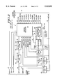
- FIG. 1 is a block diagram illustrates one embodiment of a data processing system, in accordance with the present invention
- FIG. 2 is a block diagram that illustrates a portion of processor of FIG. 1;
- FIG. 3 is a block diagram that illustrates one embodiment of a portion of coprocessor of FIG. 1;
- FIG. 4 is a timing diagram that illustrates a register snooping operation, in accordance with the present invention
- FIG. 5 is a timing diagram that illustrates the basic instruction interface operation for instruction handshaking
- FIG. 6 is a timing diagram that illustrates the Instruction interface operation when the H -- BUSY* signal is used to control coprocessor interface instruction execution;
- FIG. 7 is a timing diagram that illustrates instruction discard
- FIG. 8 is a timing diagram that illustrates an example of instruction pipeline stall
- FIG. 9 is a timing diagram that illustrates an example of back-to-back execution with no stalls
- FIG. 10 is a timing diagram that illustrates back-to-back operation with internal pipeline stalls
- FIG. 11 is a timing diagram that illustrates back-to-back coprocessor interface 30 instructions with H -- BUSY* stalls;
- FIG. 12 is a timing diagram that illustrates an example of the H -- EXCP* signal being asserted by a coprocessor in response to the decode and attempted execution of a coprocessor interface opcode;
- FIG. 13 is a timing diagram that illustrates an example of the H -- EXCP* signal being asserted by a coprocessor in response to the decode and attempted execution of a coprocessor interface opcode when the coprocessor interface instruction is discarded;
- FIG. 14 is a timing diagram that illustrates an example where H -- BUSY* has been asserted to delay the execution of an coprocessor interface opcode
- FIG. 15 is a timing diagram that illustrates an example of register transfers associated with the H -- CALL primitive.
- FIG. 16 is a timing diagram that illustrates an example of register transfers associated with the H -- RET primitive
- FIG. 17 is a timing diagram that illustrates the sequencing of an H -- LD transfer to the coprocessor interface
- FIG. 18 is a timing diagram that illustrates the protocol when a memory access results in an access exception
- FIG. 19 is a timing diagram that illustrates an example of a transfer associated with the H -- ST primitive
- FIG. 20 is a timing diagram that illustrates an example of a transfer with delayed store data
- FIG. 21 is a timing diagram that illustrates the protocol signals when the store results in an access error
- FIG. 22 illustrates an instruction format for the H -- CALL primitive, in accordance with the present invention
- FIG. 23 illustrates an instruction format for the H -- RET primitive, in accordance with the present invention
- FIG. 24 illustrates an instruction format for the H -- EXEC primitive, in accordance with the present invention.
- FIG. 25 illustrates an instruction format for the H -- LD instruction, in accordance with the present invention.
- FIG. 26 illustrates an instruction format for the H -- ST instruction, in accordance with the present invention.
- bus will be used to refer to a plurality of signals or conductors which may be used to transfer one or more various types of information, such as data, addresses, control, or status.
- assert and “negate” will be used when referring to the rendering of a signal, status bit, or similar apparatus into its logically true or logically false state, respectively. If the logically true state is a logic level one, the logically false state will be a logic level zero. And if the logically true state is a logic level zero, the logically false state will be a logic level one.
- FIG. 1 is a block diagram that illustrates one embodiment of a data processing system 10 includes a processor 12, a coprocessor 14, a coprocessor 16, a memory 18, other modules 20 and external bus interface 22 which are all bidirectionally coupled by way of bus 28. Alternate embodiments of the present invention may have only one coprocessor 14, two coprocessors 14 and 16 or even more coprocessors (not shown). External bus interface 22 is bidirectionally coupled to external bus 26 by way of integrated circuit terminals 35. Memory 24 is bidirectionally coupled to external bus 26. Processor 12 may optionally be coupled external to data processing system 10 by way of integrated circuit terminals 31. Coprocessor 14 may optionally be coupled external to data processing system 10 by way of integrated circuit terminals 32.
- Memory 18 may optionally be coupled external to data processing system 10 by way of integrated circuit terminals 32.
- Other modules 20 may optionally be coupled external to data processing system 10 by way of integrated circuit terminals 34.
- Processor 12 is bidirectionally coupled to both coprocessor 14 and coprocessor 16 by way of coprocessor interface 30.
- FIG. 2 is a block diagram that illustrates a portion of processor 12 of FIG. 1.
- processor 12 includes control circuitry 40, instruction decode circuitry 42, instruction pipe 44, registers 46, arithmetic logic unit (ALU) 48, latching multiplexer (MUX) 50, latching multiplexer (MUX) 52, and multiplexer (MUX) 54.
- coprocessor interface 30 includes signals 60-71.
- Clock signal 60 is generated by control circuitry 40.
- Coprocessor operation signals 61 are generated by control circuitry 40 and are provided to coprocessors 14 and 16.
- Supervisor mode signal 62 is generated by control circuitry 40 and is provided to coprocessors 14 and 16.
- Decode signal 63 is generated by control circuitry 40 and is provided to coprocessor 14 and 16.
- Coprocessor busy signal 64 is received by control circuitry 40 from coprocessor 14 or coprocessor 16.
- Execute signal 65 is generated by control circuitry 40 and is provided to coprocessors 14 and 16.
- Exception signal 66 is received by control circuitry 40 from coprocessor 14 or coprocessor 16.
- Register write (REGWR*) signal 67 is generated by control circuitry 40 and is provided to coprocessors 14 and 16.
- Register signals (REG ⁇ 4:0 ⁇ ) 68 are generated by control circuitry 40 and are provided to coprocessors 14 and 16.
- Error signal (H -- ERR*) 69 is generated by control circuitry 40 and is provided to coprocessors 14 and 16.
- Data strobe signal (H -- DS*) 70 is generated by control circuitry 40 and is provided to coprocessors 14 and 16.
- Data acknowledge signal (H -- DA*) 71 is received by control circuitry 40 from coprocessor 14 or coprocessor 16.
- Hardware data ports signal (HDP ⁇ 31:0 ⁇ 72 which are also considered part of coprocessor interface 30 are bi-directional between coprocessors 14 and 16 and internal circuitry within processor 12.
- a plurality of signals are provided to or from bus 28 in order to load or store data in memory 18 and/or memory 24.
- these signals include a transfer request signal (TREQ*) 73 that is generated by control circuitry 40 and provided to bus 28.
- Transfer error acknowledge signal (TEA*) 74 is provided to control circuitry 40 by way of bus 28.
- Transfer acknowledge signal (TA*) 75 is provided to control circuitry 40 by way of bus 28.
- Instructions are provided from bus 28 to instruction pipe 44 by way of conductors 76.
- Data is provided to MUX 54 by way of conductors 76.
- Drive Data signal 79 enables tristate buffer 95 to provide data from latching MUX 52 by way of conductors 88 and 76.
- Address Select signal 78 enables latching MUX 50 to provide addresses to bus 28 by way of conductors 77.
- Another input to MUX 54 is provided by the HDP signal (HDP ⁇ 31:0 ⁇ ) 72.
- Another input to MUX 54 is provided by way of the ALU result conductors 86.
- the output of MUX 54, result signals 83, are provided to registers 46 and to the input of tristate buffer 96.
- Drive HDP signal 82 enables tristate buffer 96 to drive result signals 83 on the HDP signals 72.
- the output of tristate buffer 96 is also coupled to the input of latching MUX 52. Alternate embodiments of the present invention may include any number of registers in registers 46. Result signals 83 are provided as an input to latching MUX 50.
- Result signals 83 are provided to registers 46 by way of MUX 54.
- Result Select signal (RESULT -- SELECT) 81 selects which input of MUX 54 is to be driven on result conductors 83.
- Source select signal (SOURCE -- SELECT) 80 is provided to latching MUX 52 to select which signal shall be driven to tristate buffer 95 on conductors 88.
- Control circuitry 40 provides control information and receives status information from registers 46 by way of conductors 91.
- Control circuitry 40 provides control signals and receives status signals from arithmetic logic unit 48 by way of conductors 92.
- Control circuitry 40 provides control signals and receives status signals from instruction pipe 44 and instruction decode circuitry 42 by way of conductors 93.
- Instruction pipe 44 is coupled to provide instructions to instruction decode circuitry 42 by way of conductors 89.
- Instruction decode circuitry 42 provides decoded instruction information to control circuitry 40 by way of conductors 90.
- Registers 46 provide source operands to arithmetic logic unit 48 by way of conductors 84.
- Registers 46 provide data to be stored in memory 18 or memory 24 by way of conductors 84, latching MUX 52, tristate buffer 95 and conductor 76.
- Register 46 provide address information to memory 18 or memory 24 by way of conductors 84, latching MUX 50 and address conductor 77.
- Registers 46 provide a second source operand to arithmetic logic unit 48 by way of conductors 85.
- FIG. 3 is a block diagram that illustrates one embodiment of a portion of coprocessor 14.
- coprocessor 14 includes control circuitry 100, computation circuitry 102 and optional storage circuitry 104.
- Control circuitry 100 is bidirectionally coupled to processor 12 by way of coprocessor interface 30 which includes signals 60-72.
- control circuitry 100 includes decode circuitry 106 which receives the operation signals 61 and the decode signal 63 from processor 12.
- Control circuitry 100 provides control information and receives status information from optional storage circuitry 104 by way of conductors 108.
- Control circuitry 100 provides control information and receives status information from computation circuitry 102 by way of conductors 109.
- Computation circuitry 102 and optional storage circuitry 104 are bidirectionally coupled by way of conductors 110.
- One or more of signals 110 may be provided to or from bus 28 or integrated circuit terminals 32.
- Control circuitry 100 may receive or provide information to or from bus 28 or integrated circuit terminals 32 by way of conductors 112.
- Signals 72 may be bidirectionally coupled to computation circuitry 102 and optional storage circuitry 104.
- signals 72 may be bidirectionally coupled to bus 28 or integrated circuit terminals 32.
- optional storage circuitry 104 may not be implemented. In embodiments of the present invention in which optional storage circuitry 104 is implemented, it may be implemented using registers, any type of memory, any type of storage circuit including latches or programmable logic arrays, etc.
- computation circuitry 102 may perform any type of logic or computational function.
- the system provides support for task acceleration by an external coprocessor 14 (or hardware accelerator) which is optimized for specific application related operations.
- external coprocessors 14, 16 may be as simple as a coprocessor 14 for performing a population count, or a more complicated function such as a DSP acceleration coprocessor 14 or coprocessor 14 capable of high speed multiply/accumulate operation.
- Data is transferred between the processor 12 and a coprocessor 14 by one or more of several mechanisms as appropriate for a particular implementation. These can be divided into transfers to the coprocessor 14, and transfers from the coprocessor 14.
- Register Snooping mechanism involves no instruction primitive, but is a by-product of normal processor 12 operation. This involves reflecting updates to the processor's 12 general purpose registers ("GPR") 46 across the interface such that a coprocessor 14 could monitor updates to one or more processor 12 registers. This might be appropriate if a coprocessor 14 "overlays" a GPR 46 for an internal register or function. In this case, no explicit passing of parameters from the processor 12 to a coprocessor 14 would be required.
- GPR general purpose registers
- Instruction primitives are provided in the base processor 12 for explicit transfer of operands and instructions between external coprocessors 14, 16 and the processor 12 as well.
- a handshaking mechanism is provided to allow control over the rate of instruction and data transfer.
- coprocessor 14 functions are designed to be implementation specific units, thus the exact functionality of a given unit is free to be changed across different implementations, even though the same instruction mappings may be present.
- FIG. 4 is a timing diagram that illustrates a register snooping operation.
- a register snooping mechanism is provided. This allows a coprocessor 14 to implement a shadow copy of one or more of the processor's 12 general registers 46.
- the capability is implemented by transferring the value being written into one of the processor GPRs 46 and an indication of which register 46 is being updated for each GPR update.
- a strobe signal REGWR* 67 is asserted for each register update.
- the value is transferred across the 32-bit bi-directional data path HDP 31:0! 72, and a 5-bit register number bus provides a pointer to the actual processor register 46 being updated (REG 4:0! 68.
- the register number may refer to a register 46 in a normal file or in an alternate file.
- this invention does not depend in any way on the actual partitioning of the register set.
- a coprocessor 14 may latch the value internally along with an indication of the destination register 46 number to avoid an explicit move later. This functionality may also be used by a debug coprocessor 14 to track the state of the register file 46 or a subset of it.
- FIG. 4 shows an example of the snooping capability.
- a dedicated 12-bit instruction bus (H -- OP 11:0!) 61 provides the coprocessor interface 30 opcode being issued to the external coprocessor 14. This bus reflects the low order 12 bits of the processor's opcode. The high-order four bits are not reflected as they are always 0b0100.
- a supervisor mode indicator (H -- SUP) 62 is also provided to indicate the current state of the PSR(S) bit, indicating whether the processor is operating in supervisor or user mode. This can be useful for limiting certain coprocessor functions to supervisory mode.
- a set of handshake signals between the processor 12 and external coprocessors 14, 16 coordinate coprocessor interface 30 instruction execution.
- the control signals generated by the processor 12 are a reflection of the internal pipeline structure of the processor 12.
- the processor pipeline 44 consists of stages for instruction fetch, instruction decode 42, execution, and result writeback. It contains one or more instruction registers (IR).
- the processor 12 also contains an instruction prefetch buffer to allow buffering of an instruction prior to the decode stage 42. Instructions proceed from this buffer to the instruction decode stage 42 by entering the instruction decode register IR.
- the instruction decoder 42 receives inputs from the IR, and generates outputs based on the value held in the IR. These decode 42 outputs are not always valid, and may be discarded due to exception conditions or changes in instruction flow. Even when valid, instructions may be held in the IR until they can proceed to the execute stage of the instruction pipeline. Since this cannot occur until previous instructions have completed execution (which may take multiple clocks), the decoder will continue to decode the value contained in the IR until the IR is updated.
- FIG. 5 is a timing diagram that illustrates the basic instruction interface operation for instruction handshaking.
- An instruction decode strobe (H -- DEC*) signal 63 is provided to indicate the decode of an coprocessor interface 30 opcode by the processor 12. This signal will be asserted when a coprocessor interface 30 opcode resides in the IR, even if the instruction may be discarded without execution.
- the H -- DEC* 63 output may remain asserted for multiple clocks for the same instruction until the instruction is actually issued or is discarded.
- a busy signal (H -- BUSY*) 64 is monitored by the processor 12 to determine if an external coprocessor 14 can accept the coprocessor interface 30 instruction, and partially controls when issuance of the instruction occurs. If the H -- BUSY* 64 signal is negated while H -- DEC* 63 is asserted, instruction execution will not be stalled by the interface, and the H -- EXEC* 65 signal may assert as soon as instruction execution can proceed. If the H -- BUSY* 64 signal is asserted when the processor 12 decodes an coprocessor interface 30 opcode (indicated by the assertion of H -- DEC* 63), execution of the coprocessor interface 30 opcode will be forced to stall.
- the processor 12 may issue the instruction by asserting H -- EXEC* 65. If a coprocessor 14 is capable of buffering instructions, the H -- BUSY* 64 signal may be used to assist filling of the buffer.
- FIG. 6 is a timing diagram that illustrates the Instruction interface operation when H -- BUSY* 64 is used to control coprocessor interface 30 instruction execution.
- the processor can assert H -- EXEC* 65 to indicate that the coprocessor interface 30 instruction has entered the execute stage of the pipeline.
- An external coprocessor 14 should monitor the H -- EXEC* 65 signal to control actual execution of the instruction, since it is possible for the processor to discard the instruction prior to execution in certain circumstances. If execution of an earlier instruction results in an exception being taken, the H -- EXEC* 65 signal will not be asserted, and the H -- DEC* 63 output will be negated.
- a similar process can occur if the instruction in the IR is discarded as the result of a change in program flow.
- FIG. 7 is a timing diagram that illustrates instruction discard. If an instruction is discarded, the H -- DEC* 63 signal will be negated before another coprocessor interface 30 opcode is placed on the H -- OP 11:0! 61 bus.
- FIG. 8 is a timing diagram that illustrates an example of instruction pipeline stall. There are circumstances where the processor 12 may delay the assertion of H -- EXEC* 65 even though H -- DEC* 63 is asserted and H -- BUSY* 64 is negated. This can occur while waiting for an earlier instruction to complete.
- FIG. 9 is a timing diagram that illustrates an example of back-to-back execution with no stalls.
- the H -- DEC* 63 signal can remain asserted without negation, even though the H -- OP 11:0! 61 bus is updated as new instructions enter the IR.
- the assertion of H -- EXEC* 65 corresponds to execution of the instruction being decoded on the previous clock.
- FIG. 10 is a timing diagram that illustrates back-to-back operation with internal pipeline stalls.
- H -- BUSY* 64 is negated, but the processor does not assert H -- EXEC* 65 for the second coprocessor interface 30 instruction until the internal stall condition disappears.
- FIG. 11 is a timing diagram that illustrates back-to-back coprocessor interface 30 instructions with H -- BUSY* 64 stalls.
- the external coprocessor 14 is busy, and cannot accept the second instruction immediately.
- H -- BUSY* 64 asserts to prevent the second instruction from being issued by the processor 12. Once the coprocessor 14 becomes free, H -- BUSY* 64 is negated, and the next coprocessor interface 30 instruction advances to the execute stage.
- Exceptions related to the decode of an coprocessor interface 30 opcode may be signaled by an external coprocessor 14 with the H -- EXCP* 66 signal. This input to the processor 12 is sampled during the clock cycle that H -- DEC* 63 is asserted and H -- BUSY* 64 is negated, and will result in exception processing for a Hardware Coprocessor 14 Exception if the coprocessor interface 30 opcode is not discarded as previously described. Details of this exception processing are described below.
- FIG. 12 is a timing diagram that illustrates an example of the H -- EXCP* 66 signal being asserted by a coprocessor 14 in response to the decode and attempted execution of a coprocessor interface 30 opcode.
- the H -- EXCP* 66 signal is sampled by the processor 12 during the clock that H -- DEC* 63 is asserted and H -- BUSY* 64 is negated.
- the H -- EXEC* 65 signal is asserted regardless of whether an exception is signaled by the interface; this assertion distinguishes the exception taken case from the instruction discard case.
- H -- EXCP* 66 is ignored for all clock cycles where H -- DEC* 63 is negated or H -- BUSY* 64 is asserted.
- FIG. 13 is a timing diagram that illustrates an example of the H -- EXCP* 66 signal being asserted by a coprocessor 14 in response to the decode and attempted execution of a coprocessor interface 30 opcode. Contrasting this with the timing diagram in FIG. 14, in this example, the coprocessor interface 30 instruction is discarded, so the H -- EXEC* 65 signal is not asserted, and the H -- DEC* 63 is negated.
- FIG. 14 is a timing diagram that illustrates an example where H -- BUSY* 64 has been asserted to delay the execution of an coprocessor interface 30 opcode which will result in an exception.
- H -- BUSY* 64 and H -- EXCP* 66 signals are shared by all coprocessors 14, 16, thus they must be driven in a coordinated manner. These signals should be driven (either high or low, whichever is appropriate) by the coprocessor 14, 16 corresponding to H -- OP 11:10! 61 on clock cycles where H -- DEC* 63 is asserted. By driving the output only during the low portion of the clock, these signals may be shared by multiple coprocessors 14, 16 without contention. A holding latch internal to the processor 12 is provided on this input to hold it in a valid state for the high phase of the clock while no unit is driving it.
- Some of the coprocessor interface 30 instruction primitives also imply a transfer of data items between the processor 12 and an external coprocessor 14. Operands may be transferred across the coprocessor interface 30 as a function of the particular primitive being executed. Provisions are made for transferring one or more of the processor 12 GPRs either to or from coprocessor 14 across a 32-bit bi-directional data path. In addition, provisions are also made to load or store a single data item from/to memory 18 with the data sink/source being the coprocessor interface 30.
- the processor 12 will pass parameters to external coprocessors 14, 16 via the HDP 31:0! 72 bus during the high portion of CLK 60, operands are received and latched from the coprocessor interface 30 by the processor 12 during the low phase of the clock.
- a delay is provided as the clock transitions high before drive occurs to allow for a small period of bus hand-off.
- a coprocessor 14 interface must provide the same small delay at the falling clock edge.
- Handshaking of data items is supported with the Data Strobe (H -- DS* 70) output, the Data Acknowledge (H -- DA* 71) input, and the Data Error (H -- ERR* 69) output signals.
- the processor 12 provides the capability of transferring a list of call or return parameters to the coprocessor interface 30 in much the same way as software subroutines are called or returned from.
- a count of arguments is indicated in the H -- CALL or H -- RET primitive to control the number of parameters passed.
- Register values beginning with the content of processor 12 register R4 are transferred to (from) the external coprocessor 14 as part of the execution of the H -- CALL (H -- RET) primitive. Up to seven register parameters may be passed. This convention is similar to the software subroutine calling convention.
- Handshaking of the operand transfers are controlled by the Data Strobe (H -- DS* 70) output and Data Acknowledge (H -- DA* 71) input signals.
- Data Strobe will be asserted by the processor 12 for the duration of the transfers, and transfers will occur in an overlapped manner, much the same as the processor 12 interface operation.
- Data Acknowledge (H -- DA*) 71 is used to indicate that a data element has been accepted or driven by a coprocessor 14.
- FIG. 15 is a timing diagram that illustrates an example of register 46 transfers associated with the H -- CALL primitive. Instruction primitives are provided to transfer multiple processor registers and the transfers can ideally occur every clock. For transfers to an external coprocessor 14, the processor will automatically begin driving the next operand (if needed) prior to (or concurrent with) the acknowledge of the current item. External logic must be capable of one level of buffering to ensure no loss of data.
- This FIG. shows the sequencing of an H -- CALL transfer to the coprocessor interface 30, where two registers are to be transferred. The second transfer is repeated due to a negated Data Acknowledge (H -- DA*) 71.
- H -- DA* negated Data Acknowledge
- the processor 12 For transfers from an external coprocessor 14 to processor registers 46, the processor 12 is capable of accepting values from an external coprocessor 14 every clock cycle after H -- DS* 70 has been asserted, and these values are written into the register file 46 as they are received, so no buffering is required.
- FIG. 16 is a timing diagram that illustrates an example of register 46 transfers associated with the H -- RET primitive.
- the coprocessor 14 may drive data beginning with the clock following the assertion of the H -- EXEC* 65 signal, as this is the clock where H -- DS* 70 will first be asserted.
- the H -- DS* 70 output transitions with the rising edge of CLK 60, while the H -- DA* 71 input is sampled during the low phase of CLK 60.
- the processor 12 provides the capability of transferring a single memory operand to or from the coprocessor interface 30 with the H -- LD or H -- ST instruction primitives.
- the H -- LD primitive is used to transfer data from memory 18 to a coprocessor 14. Handshaking of the operand transfer to the coprocessor 14 is controlled by the Data Strobe (H -- DS*) 70 signal. Data Strobe will be asserted by the processor 12 to indicate that a valid operand has been placed on the HDP 31:0! 72 bus. The Data Acknowledge (H -- DA*) 71 input is ignored for this transfer.
- H -- DS* Data Strobe
- FIG. 17 is a timing diagram that illustrates the sequencing of an H -- LD transfer to the coprocessor interface 30.
- the operand and H -- DS* 70 would be driven n clocks later. If the option to update the base register 46 with the effective address of the load is selected, the update value is driven on HDP 31:0! 72 the first clock after it has been calculated (the clock following the assertion of H -- EXEC* 65).
- FIG. 18 is a timing diagram that illustrates the protocol when a memory 18 access results in an access exception.
- the H -- ERR* 69 signal is asserted back to the external coprocessor 14.
- the H -- ST primitive can be used to transfer data to memory 18 from a coprocessor 14. If the option to update the base register 46 with the effective address of the store is selected, the update value is driven on HDP 31:0! 72 the first clock after it has been calculated (the clock following the assertion of H -- EXEC* 65).
- FIG. 19 is a timing diagram that illustrates an example of a transfer associated with the H -- ST primitive.
- the handshake associated with the H -- ST primitive consists of two parts, an initial handshake from the coprocessor 14, which must provide data for the store, and a completion handshake from the processor 12 once the store to memory 18 has completed.
- the initial handshake uses the H -- DA* 71 input to the processor 12 to signal that the coprocessor 14 has driven store data to the processor 12.
- the H -- DA* 71 signal is asserted the same clock that data is driven onto the HDP 31:0! 72 bus by the coprocessor 14.
- the store data is taken from the lower half of the bus for a halfword sized store, the upper 16 bits will not be written into memory 18.
- the H -- DA* 71 signal will be sampled beginning with the clock the H -- EXEC* 65 signal is asserted.
- the memory cycle is requested during the clock where H -- DA* 71 is recognized, and store data will be driven to memory 18 on the following clock. Once the store has completed, the processor 12 will assert the H -- DS* 70 signal.
- FIG. 20 is a timing diagram that illustrates an example of a transfer with delayed store data.
- FIG. 21 is a timing diagram that illustrates the protocol signals when the store results in an access error. Note here that the H -- ERR* 69 signal is asserted. If the hardware unit aborts the instruction by asserting H -- EXCP* 66 the clock where H -- EXEC* 65 is asserted, the H -- DA* 71 signal should not be asserted.
- FIGS. 22 through 26 illustrate instructions provided as part of the instruction set to interface to aHardware Accelerator (or coprocessor) 14.
- the processor 12 interprets some of the fields in the primitives, others are interpreted by the coprocessor 14 alone.
- FIG. 22 illustrates an instruction format for the H -- CALL primitive. This instruction is used to "call” a function implemented by a coprocessor 14.
- the paradigm is similar to a standard software calling convention, but in a hardware context.
- the H -- CALL primitive is interpreted by both the processor 12 and the coprocessor 14 to transfer a list of "call parameters" or arguments from the processor 12 and initiate a particular function in the coprocessor 14.
- the UU and CODE fields of the instruction word are not interpreted by the processor 12, these are used to specify a coprocessor 14 specific function.
- the UU field may specify a specific coprocessor 14, 16, and the CODE field may specify a particular operation.
- the CNT field is interpreted by both the processor 12 and the coprocessor 14, and specifies the number of register arguments to pass to the coprocessor 14.
- Arguments are passed from the general registers 46 beginning with R4 and continuing through R(4+CNT-1). Up to seven parameters or registers 46 may be passed in a single H -- CALL invocation.
- the H -- CALL instruction can be used to implement modular module invocation. Usage of this type of interface has long been known to result in software systems with higher reliability and fewer bugs. Function parameters are usually best passed by value. This significantly reduces side-effects. In many cases, modem compilers for block-structured languages such as C and C++ pass short sequences of parameters or arguments to invoked functions or subroutines in registers 46. This technique can be implemented with the H -- CALL instruction. A compiler can be configured to load up to seven parameters or arguments into successive registers 46 starting at R4, then generating the H -- CALL instruction, which replaces the standard compiler generated subroutine linkage instruction.
- FIG. 23 illustrates an instruction format for the H -- RET primitive. This instruction is used to "return from” a function implemented by a coprocessor 14. The paradigm is similar to the software calling convention used by the processor 12, but in a hardware context.
- the H -- RET primitive is interpreted by both the processor 12 and the coprocessor 14 to transfer a list of "return parameters" or values to the processor 12 from a coprocessor 14.
- the UU and CODE fields of the instruction word are not interpreted by the processor 12, these are used to specify a coprocessor 14 specific function.
- the UU field may specify a hardware unit, and the CODE field may specify a particular operation or set of registers 46 in the coprocessor 14 to return.
- the CNT field is interpreted by both the processor 12 and the coprocessor 14, and specifies the number of register 46 arguments to pass from the coprocessor 14 to the processor 12.
- Arguments are passed to the processor 12 general registers 46 beginning with R4 and continuing through R(4+CNT-1). Up to seven parameters (or register contents) may be returned.
- the H -- RET instruction can also be used to implement modular programming. Structured programming requires that function return values are best passed back to a calling routine by value. This is often done efficiently by compilers by placing one or more return values in registers for a subroutine or function return. It should be noted though that traditional structured programming expects a subroutine or function to return immediately after the subroutine or function invocation. In the case of coprocessors 14, execution is often asynchronous with that of the invoking processor 12.
- the H -- RET instruction can be used to resynchronize the processor 12 and coprocessor 14.
- the processor 12 may load one or more registers 46, activate the coprocessor 14 with one or more H -- CALL instructions, execute unrelated instructions, and then resynchronize with the coprocessor 14 while receiving a resulting value or values from the coprocssor 14 by issuing the H -- RET instruction.
- FIG. 24 illustrates an instruction format for the H -- EXEC primitive. This instruction is used to initiate a function or enter an operating mode implemented by an Accelerator.
- the H -- EXEC instruction can be used to control a function in a specific coprocessor 14, 16 specified by a UU field.
- the code field is not interpreted by the processor 12 but is rather reserved for the designated coprocessor 14, 16.
- the UU and CODE fields of the instruction word are not interpreted by the processor 12, these are used to specify a coprocessor 14 specific function.
- the UU field may specify a specific coprocessor 14, 16, and the CODE field may specify a particular operation.
- FIG. 25 illustrates an instruction format for the H -- LD instruction. This instruction is used to pass a value from memory 18 to a coprocessor 14 without temporarily storing the memory operand in a General Purpose Register (GPR) 46. The memory operand is addressed using a base pointer and an offset.
- GPR General Purpose Register
- the H -- LD instruction performs a load of a value in memory 18, and passes the memory operand to the coprocessor 14 without storing it in a register 46.
- the H -- LD operation has three options, w- word, h- half word and u- update. Disp is obtained by scaling the IMM2 field by the size of the load, and zero-extending. This value is added to the value of Register RX and a load of the specified size is performed from this address, with the result of the load passed to the hardware interface 28. For halfword loads, the data fetched is zero-extended to 32-bits. If the .u option is specified, the effective address of the load is placed in register RX 46 after it is calculated.
- the UU field of the instruction word is not interpreted by the processor 12, this field may specify a specific coprocessor 14, 16.
- the Sz field specifies the size of the operand (halfword or word only).
- the Disp field specifies an unsigned offset value to be added to the content of the register specified by the Rbase field to form the effective address for the load. The value of the Disp field is scaled by the size of the operand to be transferred.
- the Up field specifies whether the Rbase register 46 should be updated with the effective address of the load after it has been calculated. This option allows an "auto-update" addressing mode.
- FIG. 26 illustrates an instruction format for the H -- ST instruction. This instruction is used to pass a value from a coprocessor 14 to memory 18 without temporarily storing the memory operand in a processor 12 register 46. The memory operand is addressed using a base pointer and an offset.
- the UU field of the instruction word is not interpreted by the processor 12. Rather this field may specify a specific coprocessor 14, 16.
- the Sz field specifies the size of the operand (halfword or word only).
- the Disp field specifies an unsigned offset value to be added to the content of the register 46 specified by the Rbase field to form the effective address for the store. The value of the Disp field is scaled by the size of the operand to be transferred.
- the Up field specifies whether the Rbase register should be updated with the effective address of the store after it has been calculated. This option allows an "auto-update" addressing mode.
- the H -- ST instruction performs a store to memory 18, of an operand from a coprocessor 14 without storing it in a register 46.
- the H -- ST operation has three options, w- word, h- half word and u- update.
- Disp is obtained by scaling the IMM2 field by the size of the store and zero-extending. This value is added to the value of Register RX and a store of the specified size is performed to this address, with the data for the store obtained from the hardware interface. If the .u option is specified, the effective address of the load is placed in register RX after it is calculated.
- the H -- LD instruction and the H -- ST instruction provide an efficient mechanism to move operands from memory 18 to a coprocessor 14 and from a coprocessor 14 to memory 18 without the data being moved routing through registers 46.
- the offset and indexing provisions provide a mechanism for efficiently stepping through arrays. Thus, these instructions are especially useful within loops. Note should be made that both instructions synchronize the processor 12 with the coprocessor 14 for every operand loaded or stored. If this is not necessary or even preferred, one may alternatively stream data to the coprocessor 14 by repeatedly loading a designated register or registers 46 with data from memory 18, and have the coprocessor 14 detect these loads since the coprocessor interface bus 30 is also used for register snooping.
Abstract
Description
Claims (10)
Priority Applications (1)
| Application Number | Priority Date | Filing Date | Title |
|---|---|---|---|
| US08/924,137 US5923893A (en) | 1997-09-05 | 1997-09-05 | Method and apparatus for interfacing a processor to a coprocessor |
Applications Claiming Priority (1)
| Application Number | Priority Date | Filing Date | Title |
|---|---|---|---|
| US08/924,137 US5923893A (en) | 1997-09-05 | 1997-09-05 | Method and apparatus for interfacing a processor to a coprocessor |
Publications (1)
| Publication Number | Publication Date |
|---|---|
| US5923893A true US5923893A (en) | 1999-07-13 |
Family
ID=25449764
Family Applications (1)
| Application Number | Title | Priority Date | Filing Date |
|---|---|---|---|
| US08/924,137 Expired - Fee Related US5923893A (en) | 1997-09-05 | 1997-09-05 | Method and apparatus for interfacing a processor to a coprocessor |
Country Status (1)
| Country | Link |
|---|---|
| US (1) | US5923893A (en) |
Cited By (52)
| Publication number | Priority date | Publication date | Assignee | Title |
|---|---|---|---|---|
| US6163836A (en) * | 1997-08-01 | 2000-12-19 | Micron Technology, Inc. | Processor with programmable addressing modes |
| WO2001029652A2 (en) * | 1999-10-20 | 2001-04-26 | Accelerated Encryption Processing Limited | A cryptographic accelerator |
| US6226738B1 (en) | 1997-08-01 | 2001-05-01 | Micron Technology, Inc. | Split embedded DRAM processor |
| US6247113B1 (en) * | 1998-05-27 | 2001-06-12 | Arm Limited | Coprocessor opcode division by data type |
| US6434689B2 (en) * | 1998-11-09 | 2002-08-13 | Infineon Technologies North America Corp. | Data processing unit with interface for sharing registers by a processor and a coprocessor |
| US6513091B1 (en) | 1999-11-12 | 2003-01-28 | International Business Machines Corporation | Data routing using status-response signals |
| US6526469B1 (en) | 1999-11-12 | 2003-02-25 | International Business Machines Corporation | Bus architecture employing varying width uni-directional command bus |
| US6532530B1 (en) * | 1999-02-27 | 2003-03-11 | Samsung Electronics Co., Ltd. | Data processing system and method for performing enhanced pipelined operations on instructions for normal and specific functions |
| US20030061447A1 (en) * | 2000-01-05 | 2003-03-27 | Perego Richard E. | Memory system including a point-to-point linked memory subsystem |
| US6557069B1 (en) | 1999-11-12 | 2003-04-29 | International Business Machines Corporation | Processor-memory bus architecture for supporting multiple processors |
| US20030093648A1 (en) * | 2001-11-13 | 2003-05-15 | Moyer William C. | Method and apparatus for interfacing a processor to a coprocessor |
| US20030182534A1 (en) * | 2002-02-04 | 2003-09-25 | Harthcock Jerry D. | Cascaded microcomputer array and method |
| US20030187120A1 (en) * | 2002-02-20 | 2003-10-02 | Chaiko David J. | Coatings and films derived from clay/wax nanocomposites |
| WO2003088071A2 (en) * | 2002-04-10 | 2003-10-23 | Tensilica, Inc. | High-performance hybrid processor with configurable execution units |
| US20030214949A1 (en) * | 2002-05-16 | 2003-11-20 | Nadim Shaikli | System for reordering sequenced based packets in a switching network |
| US6658545B1 (en) * | 2000-02-16 | 2003-12-02 | Lucent Technologies Inc. | Passing internal bus data external to a completed system |
| US20040034760A1 (en) * | 2002-08-09 | 2004-02-19 | Paver Nigel C. | Method and apparatus for storing SIMD saturation history |
| US20040098509A1 (en) * | 2002-11-14 | 2004-05-20 | Vic Alfano | System for reordering sequenced based packet segments in a switching network |
| US20040128460A1 (en) * | 1999-12-09 | 2004-07-01 | Rambus Inc. | Transceiver with latency alignment circuitry |
| US6760833B1 (en) | 1997-08-01 | 2004-07-06 | Micron Technology, Inc. | Split embedded DRAM processor |
| US20040168041A1 (en) * | 2003-02-25 | 2004-08-26 | Internet Machines Corp. | Flexible interface device |
| US20050038975A1 (en) * | 2000-12-29 | 2005-02-17 | Mips Technologies, Inc. | Configurable co-processor interface |
| US20050044303A1 (en) * | 2000-01-05 | 2005-02-24 | Perego Richard E. | Memory system including an integrated circuit buffer device |
| US20050105516A1 (en) * | 2003-11-18 | 2005-05-19 | Heath Stewart | Switch with transparent and non-transparent ports |
| US20050117578A1 (en) * | 2003-11-18 | 2005-06-02 | Heath Stewart | Switching with transparent and non-transparent ports |
| US20050154804A1 (en) * | 2004-01-08 | 2005-07-14 | Heath Stewart | Switch for bus optimization |
| US20050166026A1 (en) * | 2000-01-05 | 2005-07-28 | Fred Ware | Configurable width buffered module having switch elements |
| US20050210221A1 (en) * | 1999-02-16 | 2005-09-22 | Renesas Technology Corp. | Microcomputer and microcomputer system |
| US6967951B2 (en) | 2002-01-11 | 2005-11-22 | Internet Machines Corp. | System for reordering sequenced based packets in a switching network |
| US20060015702A1 (en) * | 2002-08-09 | 2006-01-19 | Khan Moinul H | Method and apparatus for SIMD complex arithmetic |
| US20060149939A1 (en) * | 2002-08-09 | 2006-07-06 | Paver Nigel C | Multimedia coprocessor control mechanism including alignment or broadcast instructions |
| US7168066B1 (en) | 2001-04-30 | 2007-01-23 | Mips Technologies, Inc. | Tracing out-of order load data |
| US20070088995A1 (en) * | 2005-09-26 | 2007-04-19 | Rambus Inc. | System including a buffered memory module |
| US7237090B1 (en) | 2000-12-29 | 2007-06-26 | Mips Technologies, Inc. | Configurable out-of-order data transfer in a coprocessor interface |
| US7266634B2 (en) | 2000-01-05 | 2007-09-04 | Rambus Inc. | Configurable width buffered module having flyby elements |
| US20080034130A1 (en) * | 2000-01-05 | 2008-02-07 | Rambus Inc. | Buffered Memory Having A Control Bus And Dedicated Data Lines |
| US7356639B2 (en) | 2000-01-05 | 2008-04-08 | Rambus Inc. | Configurable width buffered module having a bypass circuit |
| GR20060100529A (en) * | 2006-09-21 | 2008-04-15 | Μιχαηλ Φωτιου Δοσης | Generalized communication method between circuits of hierarchic co-processors of special purpose. |
| US20080180450A1 (en) * | 1997-12-23 | 2008-07-31 | Micron Technology, Inc. | Split Embedded DRAM Processor |
| US20080195845A1 (en) * | 2005-01-07 | 2008-08-14 | Freescale Semiconductor, Inc. | Data processing system having flexible instruction capability and selection mechanism |
| US20080235713A1 (en) * | 2007-03-23 | 2008-09-25 | Bigfoot Networks, Inc. | Distributed Processing System and Method |
| US7562271B2 (en) | 2005-09-26 | 2009-07-14 | Rambus Inc. | Memory system topologies including a buffer device and an integrated circuit memory device |
| US20100153686A1 (en) * | 2008-12-17 | 2010-06-17 | Michael Frank | Coprocessor Unit with Shared Instruction Stream |
| US7782849B2 (en) | 2001-10-03 | 2010-08-24 | Forestay Research, Llc | Data switch and switch fabric |
| EP2278453A1 (en) * | 1999-10-15 | 2011-01-26 | Fujitsu Limited | Processor system with coprocessor |
| US7990987B2 (en) | 2003-02-25 | 2011-08-02 | Topside Research, Llc | Network processor having bypass capability |
| US20120147016A1 (en) * | 2009-08-26 | 2012-06-14 | The University Of Tokyo | Image processing device and image processing method |
| US20150268960A1 (en) * | 2014-03-18 | 2015-09-24 | Imagination Technologies Limited | Efficient calling of functions on a processor |
| US9703603B1 (en) | 2016-04-25 | 2017-07-11 | Nxp Usa, Inc. | System and method for executing accelerator call |
| US10031773B2 (en) | 2014-02-20 | 2018-07-24 | Nxp Usa, Inc. | Method to communicate task context information and device therefor |
| US11328764B2 (en) | 2005-09-26 | 2022-05-10 | Rambus Inc. | Memory system topologies including a memory die stack |
| US20230221961A1 (en) * | 2022-01-10 | 2023-07-13 | Cisco Technology, Inc. | Remote front-drop for recovery after pipeline stall |
Citations (20)
| Publication number | Priority date | Publication date | Assignee | Title |
|---|---|---|---|---|
| US4270167A (en) * | 1978-06-30 | 1981-05-26 | Intel Corporation | Apparatus and method for cooperative and concurrent coprocessing of digital information |
| US4509116A (en) * | 1982-04-21 | 1985-04-02 | Digital Equipment Corporation | Special instruction processing unit for data processing system |
| US4547849A (en) * | 1981-12-09 | 1985-10-15 | Glenn Louie | Interface between a microprocessor and a coprocessor |
| US4715013A (en) * | 1983-04-18 | 1987-12-22 | Motorola, Inc. | Coprocessor instruction format |
| US4729094A (en) * | 1983-04-18 | 1988-03-01 | Motorola, Inc. | Method and apparatus for coordinating execution of an instruction by a coprocessor |
| US4731736A (en) * | 1983-04-18 | 1988-03-15 | Motorola, Inc. | Method and apparatus for coordinating execution of an instruction by a selected coprocessor |
| US4949241A (en) * | 1987-10-22 | 1990-08-14 | Nec Corporation | Microcomputer system including a master processor and a slave processor synchronized by three control lines |
| US4979102A (en) * | 1987-12-03 | 1990-12-18 | Nec Corporation | Microprocessor operable under direct connection to coprocessor |
| US4991078A (en) * | 1987-09-29 | 1991-02-05 | Digital Equipment Corporation | Apparatus and method for a pipelined central processing unit in a data processing system |
| US5001624A (en) * | 1987-02-13 | 1991-03-19 | Harrell Hoffman | Processor controlled DMA controller for transferring instruction and data from memory to coprocessor |
| US5093908A (en) * | 1989-04-17 | 1992-03-03 | International Business Machines Corporation | Method and apparatus for executing instructions in a single sequential instruction stream in a main processor and a coprocessor |
| US5465376A (en) * | 1989-05-15 | 1995-11-07 | Mitsubishi Denki Kabushiki Kaisha | Microprocessor, coprocessor and data processing system using them |
| US5499363A (en) * | 1989-02-03 | 1996-03-12 | Nec Corporation | Microprocessor coupled to coprocessor by coprocessor bus separate from system bus to external memory for increased efficiency |
| US5504912A (en) * | 1987-04-17 | 1996-04-02 | Hitachi, Ltd. | Coprocessor executing pipeline control for executing protocols and instructions |
| US5560029A (en) * | 1991-07-22 | 1996-09-24 | Massachusetts Institute Of Technology | Data processing system with synchronization coprocessor for multiple threads |
| US5577250A (en) * | 1992-02-18 | 1996-11-19 | Apple Computer, Inc. | Programming model for a coprocessor on a computer system |
| US5603047A (en) * | 1995-10-06 | 1997-02-11 | Lsi Logic Corporation | Superscalar microprocessor architecture |
| US5640588A (en) * | 1991-05-15 | 1997-06-17 | Ross Technology, Inc. | CPU architecture performing dynamic instruction scheduling at time of execution within single clock cycle |
| US5675777A (en) * | 1990-01-29 | 1997-10-07 | Hipercore, Inc. | Architecture for minimal instruction set computing system |
| US5764939A (en) * | 1995-10-06 | 1998-06-09 | Lsi Logic Corporation | RISC processor having coprocessor for executing circular mask instruction |
-
1997
- 1997-09-05 US US08/924,137 patent/US5923893A/en not_active Expired - Fee Related
Patent Citations (20)
| Publication number | Priority date | Publication date | Assignee | Title |
|---|---|---|---|---|
| US4270167A (en) * | 1978-06-30 | 1981-05-26 | Intel Corporation | Apparatus and method for cooperative and concurrent coprocessing of digital information |
| US4547849A (en) * | 1981-12-09 | 1985-10-15 | Glenn Louie | Interface between a microprocessor and a coprocessor |
| US4509116A (en) * | 1982-04-21 | 1985-04-02 | Digital Equipment Corporation | Special instruction processing unit for data processing system |
| US4715013A (en) * | 1983-04-18 | 1987-12-22 | Motorola, Inc. | Coprocessor instruction format |
| US4729094A (en) * | 1983-04-18 | 1988-03-01 | Motorola, Inc. | Method and apparatus for coordinating execution of an instruction by a coprocessor |
| US4731736A (en) * | 1983-04-18 | 1988-03-15 | Motorola, Inc. | Method and apparatus for coordinating execution of an instruction by a selected coprocessor |
| US5001624A (en) * | 1987-02-13 | 1991-03-19 | Harrell Hoffman | Processor controlled DMA controller for transferring instruction and data from memory to coprocessor |
| US5504912A (en) * | 1987-04-17 | 1996-04-02 | Hitachi, Ltd. | Coprocessor executing pipeline control for executing protocols and instructions |
| US4991078A (en) * | 1987-09-29 | 1991-02-05 | Digital Equipment Corporation | Apparatus and method for a pipelined central processing unit in a data processing system |
| US4949241A (en) * | 1987-10-22 | 1990-08-14 | Nec Corporation | Microcomputer system including a master processor and a slave processor synchronized by three control lines |
| US4979102A (en) * | 1987-12-03 | 1990-12-18 | Nec Corporation | Microprocessor operable under direct connection to coprocessor |
| US5499363A (en) * | 1989-02-03 | 1996-03-12 | Nec Corporation | Microprocessor coupled to coprocessor by coprocessor bus separate from system bus to external memory for increased efficiency |
| US5093908A (en) * | 1989-04-17 | 1992-03-03 | International Business Machines Corporation | Method and apparatus for executing instructions in a single sequential instruction stream in a main processor and a coprocessor |
| US5465376A (en) * | 1989-05-15 | 1995-11-07 | Mitsubishi Denki Kabushiki Kaisha | Microprocessor, coprocessor and data processing system using them |
| US5675777A (en) * | 1990-01-29 | 1997-10-07 | Hipercore, Inc. | Architecture for minimal instruction set computing system |
| US5640588A (en) * | 1991-05-15 | 1997-06-17 | Ross Technology, Inc. | CPU architecture performing dynamic instruction scheduling at time of execution within single clock cycle |
| US5560029A (en) * | 1991-07-22 | 1996-09-24 | Massachusetts Institute Of Technology | Data processing system with synchronization coprocessor for multiple threads |
| US5577250A (en) * | 1992-02-18 | 1996-11-19 | Apple Computer, Inc. | Programming model for a coprocessor on a computer system |
| US5603047A (en) * | 1995-10-06 | 1997-02-11 | Lsi Logic Corporation | Superscalar microprocessor architecture |
| US5764939A (en) * | 1995-10-06 | 1998-06-09 | Lsi Logic Corporation | RISC processor having coprocessor for executing circular mask instruction |
Non-Patent Citations (6)
| Title |
|---|
| Motorola Inc. 1990, "M68300 Family CPU32 Central Processor Unit Reference Manual", Section 7 Development Support, pp. 7-1 through 7-31. |
| Motorola Inc. 1990, M68300 Family CPU32 Central Processor Unit Reference Manual , Section 7 Development Support, pp. 7 1 through 7 31. * |
| Motorola Inc. 1995, "DSP56300 24-Bit Digital Signal Processor Family Manual", Section 10 On-Chip Emulator (OnCE™), pp. 10-1 through 10-29. |
| Motorola Inc. 1995, "DSP56300 24-Bit Digital Signal Processor Family Manual", Section 11 JTAG (IEEE 1149.1) Test Access Port, pp. 11-1 through 11-9. |
| Motorola Inc. 1995, DSP56300 24 Bit Digital Signal Processor Family Manual , Section 10 On Chip Emulator (OnCE ), pp. 10 1 through 10 29. * |
| Motorola Inc. 1995, DSP56300 24 Bit Digital Signal Processor Family Manual , Section 11 JTAG (IEEE 1149.1) Test Access Port, pp. 11 1 through 11 9. * |
Cited By (151)
| Publication number | Priority date | Publication date | Assignee | Title |
|---|---|---|---|---|
| US7395409B2 (en) | 1997-08-01 | 2008-07-01 | Micron Technology, Inc. | Split embedded DRAM processor |
| US6823505B1 (en) | 1997-08-01 | 2004-11-23 | Micron Technology, Inc. | Processor with programmable addressing modes |
| US6226738B1 (en) | 1997-08-01 | 2001-05-01 | Micron Technology, Inc. | Split embedded DRAM processor |
| US6760833B1 (en) | 1997-08-01 | 2004-07-06 | Micron Technology, Inc. | Split embedded DRAM processor |
| US20040250045A1 (en) * | 1997-08-01 | 2004-12-09 | Dowling Eric M. | Split embedded dram processor |
| US6163836A (en) * | 1997-08-01 | 2000-12-19 | Micron Technology, Inc. | Processor with programmable addressing modes |
| US8489861B2 (en) | 1997-12-23 | 2013-07-16 | Round Rock Research, Llc | Split embedded DRAM processor |
| US20080180450A1 (en) * | 1997-12-23 | 2008-07-31 | Micron Technology, Inc. | Split Embedded DRAM Processor |
| US6247113B1 (en) * | 1998-05-27 | 2001-06-12 | Arm Limited | Coprocessor opcode division by data type |
| US6434689B2 (en) * | 1998-11-09 | 2002-08-13 | Infineon Technologies North America Corp. | Data processing unit with interface for sharing registers by a processor and a coprocessor |
| US20050210221A1 (en) * | 1999-02-16 | 2005-09-22 | Renesas Technology Corp. | Microcomputer and microcomputer system |
| US6532530B1 (en) * | 1999-02-27 | 2003-03-11 | Samsung Electronics Co., Ltd. | Data processing system and method for performing enhanced pipelined operations on instructions for normal and specific functions |
| EP2278453A1 (en) * | 1999-10-15 | 2011-01-26 | Fujitsu Limited | Processor system with coprocessor |
| WO2001029652A3 (en) * | 1999-10-20 | 2002-01-10 | Accelerated Encryption Proc Lt | A cryptographic accelerator |
| WO2001029652A2 (en) * | 1999-10-20 | 2001-04-26 | Accelerated Encryption Processing Limited | A cryptographic accelerator |
| US6963979B2 (en) | 1999-10-20 | 2005-11-08 | Aep Systems Limited | Cryptographic accelerator |
| US6557069B1 (en) | 1999-11-12 | 2003-04-29 | International Business Machines Corporation | Processor-memory bus architecture for supporting multiple processors |
| US6526469B1 (en) | 1999-11-12 | 2003-02-25 | International Business Machines Corporation | Bus architecture employing varying width uni-directional command bus |
| US6513091B1 (en) | 1999-11-12 | 2003-01-28 | International Business Machines Corporation | Data routing using status-response signals |
| USRE44342E1 (en) | 1999-11-12 | 2013-07-02 | International Business Machine Corporation | Bus architecture employing varying width uni-directional command bus |
| US7065622B2 (en) | 1999-12-09 | 2006-06-20 | Rambus Inc. | Transceiver with latency alignment circuitry |
| US8086812B2 (en) | 1999-12-09 | 2011-12-27 | Rambus Inc. | Transceiver with latency alignment circuitry |
| US20040128460A1 (en) * | 1999-12-09 | 2004-07-01 | Rambus Inc. | Transceiver with latency alignment circuitry |
| US7010658B2 (en) | 1999-12-09 | 2006-03-07 | Rambus Inc. | Transceiver with latency alignment circuitry |
| US20050149685A1 (en) * | 1999-12-09 | 2005-07-07 | Kevin Donnelly | Transceiver with latency alignment circuitry |
| US7124270B2 (en) | 1999-12-09 | 2006-10-17 | Rambus Inc. | Transceiver with latency alignment circuitry |
| US20070011426A1 (en) * | 1999-12-09 | 2007-01-11 | Rambus Inc. | Transceiver with latency alignment circuitry |
| US20050160247A1 (en) * | 1999-12-09 | 2005-07-21 | Dillon John B. | Transceiver with latency alignment circuitry |
| US20050193163A1 (en) * | 2000-01-05 | 2005-09-01 | Perego Richard E. | Integrated circuit buffer device |
| US20050223179A1 (en) * | 2000-01-05 | 2005-10-06 | Perego Richard E | Buffer device and method of operation in a buffer device |
| US20080034130A1 (en) * | 2000-01-05 | 2008-02-07 | Rambus Inc. | Buffered Memory Having A Control Bus And Dedicated Data Lines |
| US20050041504A1 (en) * | 2000-01-05 | 2005-02-24 | Perego Richard E. | Method of operating a memory system including an integrated circuit buffer device |
| US20050149662A1 (en) * | 2000-01-05 | 2005-07-07 | Perego Richard E. | System having a plurality of integrated circuit buffer devices |
| US7266634B2 (en) | 2000-01-05 | 2007-09-04 | Rambus Inc. | Configurable width buffered module having flyby elements |
| US20050156934A1 (en) * | 2000-01-05 | 2005-07-21 | Perego Richard E. | System featuring memory modules that include an integrated circuit buffer devices |
| US20050044303A1 (en) * | 2000-01-05 | 2005-02-24 | Perego Richard E. | Memory system including an integrated circuit buffer device |
| US7356639B2 (en) | 2000-01-05 | 2008-04-08 | Rambus Inc. | Configurable width buffered module having a bypass circuit |
| US7363422B2 (en) | 2000-01-05 | 2008-04-22 | Rambus Inc. | Configurable width buffered module |
| US20050166026A1 (en) * | 2000-01-05 | 2005-07-28 | Fred Ware | Configurable width buffered module having switch elements |
| US7320047B2 (en) | 2000-01-05 | 2008-01-15 | Rambus Inc. | System having a controller device, a buffer device and a plurality of memory devices |
| US20050210196A1 (en) * | 2000-01-05 | 2005-09-22 | Perego Richard E | Memory module having an integrated circuit buffer device |
| US20080109596A1 (en) * | 2000-01-05 | 2008-05-08 | Rambus Inc. | System Having A Controller Device, A Buffer Device And A Plurality Of Memory Devices |
| US20050207255A1 (en) * | 2000-01-05 | 2005-09-22 | Perego Richard E | System having a controller device, a buffer device and a plurality of memory devices |
| US7523248B2 (en) | 2000-01-05 | 2009-04-21 | Rambus Inc. | System having a controller device, a buffer device and a plurality of memory devices |
| US7206896B2 (en) | 2000-01-05 | 2007-04-17 | Rambus Inc. | Integrated circuit buffer device |
| US7206897B2 (en) | 2000-01-05 | 2007-04-17 | Rambus Inc. | Memory module having an integrated circuit buffer device |
| US7526597B2 (en) | 2000-01-05 | 2009-04-28 | Rambus Inc. | Buffered memory having a control bus and dedicated data lines |
| US7000062B2 (en) | 2000-01-05 | 2006-02-14 | Rambus Inc. | System and method featuring a controller device and a memory module that includes an integrated circuit buffer device and a plurality of integrated circuit memory devices |
| US7003618B2 (en) | 2000-01-05 | 2006-02-21 | Rambus Inc. | System featuring memory modules that include an integrated circuit buffer devices |
| US7010642B2 (en) | 2000-01-05 | 2006-03-07 | Rambus Inc. | System featuring a controller device and a memory module that includes an integrated circuit buffer device and a plurality of integrated circuit memory devices |
| US7200710B2 (en) | 2000-01-05 | 2007-04-03 | Rambus Inc. | Buffer device and method of operation in a buffer device |
| US7017002B2 (en) | 2000-01-05 | 2006-03-21 | Rambus, Inc. | System featuring a master device, a buffer device and a plurality of integrated circuit memory devices |
| US20060067141A1 (en) * | 2000-01-05 | 2006-03-30 | Perego Richard E | Integrated circuit buffer device |
| US20030061447A1 (en) * | 2000-01-05 | 2003-03-27 | Perego Richard E. | Memory system including a point-to-point linked memory subsystem |
| US7051151B2 (en) | 2000-01-05 | 2006-05-23 | Rambus Inc. | Integrated circuit buffer device |
| US7062597B2 (en) | 2000-01-05 | 2006-06-13 | Rambus Inc. | Integrated circuit buffer device |
| US7404032B2 (en) | 2000-01-05 | 2008-07-22 | Rambus Inc. | Configurable width buffered module having switch elements |
| US6658545B1 (en) * | 2000-02-16 | 2003-12-02 | Lucent Technologies Inc. | Passing internal bus data external to a completed system |
| US7886129B2 (en) | 2000-12-29 | 2011-02-08 | Mips Technologies, Inc. | Configurable co-processor interface |
| US7698533B2 (en) | 2000-12-29 | 2010-04-13 | Mips Technologies, Inc. | Configurable co-processor interface |
| US7287147B1 (en) * | 2000-12-29 | 2007-10-23 | Mips Technologies, Inc. | Configurable co-processor interface |
| US7194599B2 (en) | 2000-12-29 | 2007-03-20 | Mips Technologies, Inc. | Configurable co-processor interface |
| US20050038975A1 (en) * | 2000-12-29 | 2005-02-17 | Mips Technologies, Inc. | Configurable co-processor interface |
| US20070192567A1 (en) * | 2000-12-29 | 2007-08-16 | Mips Technologies, Inc. | Configurable co-processor interface |
| US7237090B1 (en) | 2000-12-29 | 2007-06-26 | Mips Technologies, Inc. | Configurable out-of-order data transfer in a coprocessor interface |
| US7168066B1 (en) | 2001-04-30 | 2007-01-23 | Mips Technologies, Inc. | Tracing out-of order load data |
| US7782849B2 (en) | 2001-10-03 | 2010-08-24 | Forestay Research, Llc | Data switch and switch fabric |
| US20030093648A1 (en) * | 2001-11-13 | 2003-05-15 | Moyer William C. | Method and apparatus for interfacing a processor to a coprocessor |
| US7228401B2 (en) * | 2001-11-13 | 2007-06-05 | Freescale Semiconductor, Inc. | Interfacing a processor to a coprocessor in which the processor selectively broadcasts to or selectively alters an execution mode of the coprocessor |
| US6967951B2 (en) | 2002-01-11 | 2005-11-22 | Internet Machines Corp. | System for reordering sequenced based packets in a switching network |
| US7856011B2 (en) | 2002-01-11 | 2010-12-21 | Vic Alfano | Reordering packets |
| US8107377B2 (en) | 2002-01-11 | 2012-01-31 | Bunson Bell, Llc | Reordering packets |
| US20060072578A1 (en) * | 2002-01-11 | 2006-04-06 | Vic Alfano | Reordering packets |
| US8913618B2 (en) | 2002-01-11 | 2014-12-16 | Bunson Bell, Limited Liability Company | Reordering packets |
| US20100189123A1 (en) * | 2002-01-11 | 2010-07-29 | Vic Alfano | Reordering Packets |
| US7073048B2 (en) * | 2002-02-04 | 2006-07-04 | Silicon Lease, L.L.C. | Cascaded microcomputer array and method |
| US20030182534A1 (en) * | 2002-02-04 | 2003-09-25 | Harthcock Jerry D. | Cascaded microcomputer array and method |
| US20030187120A1 (en) * | 2002-02-20 | 2003-10-02 | Chaiko David J. | Coatings and films derived from clay/wax nanocomposites |
| GB2402787B (en) * | 2002-04-10 | 2005-07-27 | Tensilica Inc | High-performance hybrid processor with configurable execution units |
| US20050166038A1 (en) * | 2002-04-10 | 2005-07-28 | Albert Wang | High-performance hybrid processor with configurable execution units |
| WO2003088071A2 (en) * | 2002-04-10 | 2003-10-23 | Tensilica, Inc. | High-performance hybrid processor with configurable execution units |
| GB2402787A (en) * | 2002-04-10 | 2004-12-15 | Tensilica Inc | High-performance hybrid processor with configurable execution units |
| WO2003088071A3 (en) * | 2002-04-10 | 2004-07-22 | Tensilica Inc | High-performance hybrid processor with configurable execution units |
| US7200735B2 (en) | 2002-04-10 | 2007-04-03 | Tensilica, Inc. | High-performance hybrid processor with configurable execution units |
| US20070081558A1 (en) * | 2002-05-16 | 2007-04-12 | Nadim Shaikli | System For Reordering Sequenced Based Packets In A Switching Network |
| US7668187B2 (en) | 2002-05-16 | 2010-02-23 | Topside Research, Llc | Method for reordering sequenced packets |
| US20030214949A1 (en) * | 2002-05-16 | 2003-11-20 | Nadim Shaikli | System for reordering sequenced based packets in a switching network |
| US7646780B2 (en) | 2002-05-16 | 2010-01-12 | Topside Research, Llc | System for reordering sequenced based packets in a switching network |
| US20070081539A1 (en) * | 2002-05-16 | 2007-04-12 | Nadim Shaikli | Method For Reordering Sequenced Packets |
| US20040034760A1 (en) * | 2002-08-09 | 2004-02-19 | Paver Nigel C. | Method and apparatus for storing SIMD saturation history |
| US20060149939A1 (en) * | 2002-08-09 | 2006-07-06 | Paver Nigel C | Multimedia coprocessor control mechanism including alignment or broadcast instructions |
| US7664930B2 (en) | 2002-08-09 | 2010-02-16 | Marvell International Ltd | Add-subtract coprocessor instruction execution on complex number components with saturation and conditioned on main processor condition flags |
| US20080209187A1 (en) * | 2002-08-09 | 2008-08-28 | Marvell International Ltd. | Storing and processing SIMD saturation history flags and data size |
| US8131981B2 (en) | 2002-08-09 | 2012-03-06 | Marvell International Ltd. | SIMD processor performing fractional multiply operation with saturation history data processing to generate condition code flags |
| US7392368B2 (en) | 2002-08-09 | 2008-06-24 | Marvell International Ltd. | Cross multiply and add instruction and multiply and subtract instruction SIMD execution on real and imaginary components of a plurality of complex data elements |
| US7373488B2 (en) | 2002-08-09 | 2008-05-13 | Marvell International Ltd. | Processing for associated data size saturation flag history stored in SIMD coprocessor register using mask and test values |
| US20080270768A1 (en) * | 2002-08-09 | 2008-10-30 | Marvell International Ltd., | Method and apparatus for SIMD complex Arithmetic |
| US7356676B2 (en) | 2002-08-09 | 2008-04-08 | Marvell International Ltd. | Extracting aligned data from two source registers without shifting by executing coprocessor instruction with mode bit for deriving offset from immediate or register |
| US20070204132A1 (en) * | 2002-08-09 | 2007-08-30 | Marvell International Ltd. | Storing and processing SIMD saturation history flags and data size |
| US20060015702A1 (en) * | 2002-08-09 | 2006-01-19 | Khan Moinul H | Method and apparatus for SIMD complex arithmetic |
| US7213128B2 (en) * | 2002-08-09 | 2007-05-01 | Marvell International Ltd. | Storing and transferring SIMD saturation history flags and data size |
| US20040098509A1 (en) * | 2002-11-14 | 2004-05-20 | Vic Alfano | System for reordering sequenced based packet segments in a switching network |
| US20070237151A1 (en) * | 2002-11-14 | 2007-10-11 | Vic Alfano | Reordering Sequence Based Channels |
| US7590721B2 (en) | 2002-11-14 | 2009-09-15 | Topside Research, Llc | Reordering sequence based channels |
| US20040168041A1 (en) * | 2003-02-25 | 2004-08-26 | Internet Machines Corp. | Flexible interface device |
| US7990987B2 (en) | 2003-02-25 | 2011-08-02 | Topside Research, Llc | Network processor having bypass capability |
| US8190858B2 (en) | 2003-02-25 | 2012-05-29 | Topside Research, Llc | Interface device for interfacing a main processor to processing engines and classifier engines, and methods for configuring and operating interface devices |
| US7454552B2 (en) | 2003-11-18 | 2008-11-18 | Topside Research, Llc | Switch with transparent and non-transparent ports |
| US20080304504A1 (en) * | 2003-11-18 | 2008-12-11 | Heath Stewart | PCI Express Switch with Backwards Compatibility |
| US7421532B2 (en) | 2003-11-18 | 2008-09-02 | Topside Research, Llc | Switching with transparent and non-transparent ports |
| US7945722B2 (en) | 2003-11-18 | 2011-05-17 | Internet Machines, Llc | Routing data units between different address domains |
| US20050117578A1 (en) * | 2003-11-18 | 2005-06-02 | Heath Stewart | Switching with transparent and non-transparent ports |
| US7814259B2 (en) | 2003-11-18 | 2010-10-12 | Internet Machines, Llc | PCI express switch with backwards compatibility |
| US20050105516A1 (en) * | 2003-11-18 | 2005-05-19 | Heath Stewart | Switch with transparent and non-transparent ports |
| US20110016258A1 (en) * | 2003-11-18 | 2011-01-20 | Heath Stewart | Routing Data Units Between Different Address Domains |
| US7590791B2 (en) | 2004-01-08 | 2009-09-15 | Topside Research, Llc | Optimized switching method |
| US7426602B2 (en) | 2004-01-08 | 2008-09-16 | Topside Research, Llc | Switch for bus optimization |
| US20080307150A1 (en) * | 2004-01-08 | 2008-12-11 | Heath Stewart | Optimized Switching Method |
| US20050154804A1 (en) * | 2004-01-08 | 2005-07-14 | Heath Stewart | Switch for bus optimization |
| US20080195845A1 (en) * | 2005-01-07 | 2008-08-14 | Freescale Semiconductor, Inc. | Data processing system having flexible instruction capability and selection mechanism |
| US11043258B2 (en) | 2005-09-26 | 2021-06-22 | Rambus Inc. | Memory system topologies including a memory die stack |
| US11328764B2 (en) | 2005-09-26 | 2022-05-10 | Rambus Inc. | Memory system topologies including a memory die stack |
| US9563583B2 (en) | 2005-09-26 | 2017-02-07 | Rambus Inc. | Memory system topologies including a buffer device and an integrated circuit memory device |
| US7464225B2 (en) | 2005-09-26 | 2008-12-09 | Rambus Inc. | Memory module including a plurality of integrated circuit memory devices and a plurality of buffer devices in a matrix topology |
| US10672458B1 (en) | 2005-09-26 | 2020-06-02 | Rambus Inc. | Memory system topologies including a buffer device and an integrated circuit memory device |
| US7562271B2 (en) | 2005-09-26 | 2009-07-14 | Rambus Inc. | Memory system topologies including a buffer device and an integrated circuit memory device |
| US8108607B2 (en) | 2005-09-26 | 2012-01-31 | Rambus Inc. | Memory system topologies including a buffer device and an integrated circuit memory device |
| US10535398B2 (en) | 2005-09-26 | 2020-01-14 | Rambus Inc. | Memory system topologies including a buffer device and an integrated circuit memory device |
| US7729151B2 (en) | 2005-09-26 | 2010-06-01 | Rambus Inc. | System including a buffered memory module |
| US11727982B2 (en) | 2005-09-26 | 2023-08-15 | Rambus Inc. | Memory system topologies including a memory die stack |
| US7685364B2 (en) | 2005-09-26 | 2010-03-23 | Rambus Inc. | Memory system topologies including a buffer device and an integrated circuit memory device |
| US20080144411A1 (en) * | 2005-09-26 | 2008-06-19 | Rambus Inc. | Memory Module Including A Plurality Of Integrated Circuit Memory Devices And A Plurality Of Buffer Devices In A Matrix Topology |
| US20070088995A1 (en) * | 2005-09-26 | 2007-04-19 | Rambus Inc. | System including a buffered memory module |
| US8539152B2 (en) | 2005-09-26 | 2013-09-17 | Rambus Inc. | Memory system topologies including a buffer device and an integrated circuit memory device |
| US10381067B2 (en) | 2005-09-26 | 2019-08-13 | Rambus Inc. | Memory system topologies including a buffer device and an integrated circuit memory device |
| US9117035B2 (en) | 2005-09-26 | 2015-08-25 | Rambus Inc. | Memory system topologies including a buffer device and an integrated circuit memory device |
| US9865329B2 (en) | 2005-09-26 | 2018-01-09 | Rambus Inc. | Memory system topologies including a buffer device and an integrated circuit memory device |
| GR20060100529A (en) * | 2006-09-21 | 2008-04-15 | Μιχαηλ Φωτιου Δοσης | Generalized communication method between circuits of hierarchic co-processors of special purpose. |
| US20080235713A1 (en) * | 2007-03-23 | 2008-09-25 | Bigfoot Networks, Inc. | Distributed Processing System and Method |
| US8255919B2 (en) * | 2007-03-23 | 2012-08-28 | Qualcomm Atheros, Inc. | Distributed processing system and method |
| EP2140350A1 (en) * | 2007-03-23 | 2010-01-06 | Bigfoot Networks, Inc. | Distributed processing system and method |
| EP2140350B1 (en) * | 2007-03-23 | 2017-04-05 | Qualcomm Incorporated | Distributed processing method and computer program product |
| US20100153686A1 (en) * | 2008-12-17 | 2010-06-17 | Michael Frank | Coprocessor Unit with Shared Instruction Stream |
| US7930519B2 (en) | 2008-12-17 | 2011-04-19 | Advanced Micro Devices, Inc. | Processor with coprocessor interfacing functional unit for forwarding result from coprocessor to retirement unit |
| US20120147016A1 (en) * | 2009-08-26 | 2012-06-14 | The University Of Tokyo | Image processing device and image processing method |
| US10031773B2 (en) | 2014-02-20 | 2018-07-24 | Nxp Usa, Inc. | Method to communicate task context information and device therefor |
| US20150268960A1 (en) * | 2014-03-18 | 2015-09-24 | Imagination Technologies Limited | Efficient calling of functions on a processor |
| US10528365B2 (en) * | 2014-03-18 | 2020-01-07 | Imagination Technologies Limited | Function evaluation using multiple values loaded into registers by a single instruction |
| US11656880B2 (en) | 2014-03-18 | 2023-05-23 | Nordic Semiconductor Asa | Function evaluation using multiple values loaded into registers by a single instruction |
| US9703603B1 (en) | 2016-04-25 | 2017-07-11 | Nxp Usa, Inc. | System and method for executing accelerator call |
| US20230221961A1 (en) * | 2022-01-10 | 2023-07-13 | Cisco Technology, Inc. | Remote front-drop for recovery after pipeline stall |
Similar Documents
| Publication | Publication Date | Title |
|---|---|---|
| US5923893A (en) | Method and apparatus for interfacing a processor to a coprocessor | |
| US6505290B1 (en) | Method and apparatus for interfacing a processor to a coprocessor | |
| US5983338A (en) | Method and apparatus for interfacing a processor to a coprocessor for communicating register write information | |
| KR100323191B1 (en) | Data processing device with multiple instruction sets | |
| KR100236527B1 (en) | Single instruction multiple data processing using multiple banks of vector registers | |
| US5293592A (en) | Decoder for pipelined system having portion indicating type of address generation and other portion controlling address generation within pipeline | |
| US5978838A (en) | Coordination and synchronization of an asymmetric, single-chip, dual multiprocessor | |
| EP1001335B1 (en) | Data processing unit with coprocessor interface | |
| US5440747A (en) | Data processor with control logic for storing operation mode status and associated method | |
| US5822779A (en) | Microprocessor-based data processing apparatus that commences a next overlapping cycle when a ready signal is detected not to be active | |
| JPH0774991B2 (en) | Operating method of pipelined processing unit in digital computer | |
| JPH04309131A (en) | Microcode generating apparatus for instruction group and combining apparatus in computer | |
| JP2004171573A (en) | Coprocessor extension architecture built by using novel splint-instruction transaction model | |
| JP2001142692A (en) | Microprocessor to execute two different fixed length instruction sets, microcomputer and instruction executing method | |
| JPH02140830A (en) | Micro instruction addressing for fast central arithmetic processor | |
| US5062041A (en) | Processor/coprocessor interface apparatus including microinstruction clock synchronization | |
| US6449712B1 (en) | Emulating execution of smaller fixed-length branch/delay slot instructions with a sequence of larger fixed-length instructions | |
| US6055628A (en) | Microprocessor with a nestable delayed branch instruction without branch related pipeline interlocks | |
| JPH07120284B2 (en) | Data processing device | |
| JPH09237184A (en) | Instruction executing method and its device | |
| KR100267089B1 (en) | Single instruction multiple data processing with combined scalar/vector operations | |
| US20060095723A1 (en) | Method and apparatus for interfacing a processor to a coprocessor | |
| US5737562A (en) | CPU pipeline having queuing stage to facilitate branch instructions | |
| GB2230116A (en) | Pipelined instruction decoding apparatus | |
| JP3547585B2 (en) | Microprocessor having conditional execution instruction |
Legal Events
| Date | Code | Title | Description |
|---|---|---|---|
| AS | Assignment |
Owner name: MOTOROLA, INC., ILLINOIS Free format text: ASSIGNMENT OF ASSIGNORS INTEREST;ASSIGNORS:MOYER, WILLIAM C.;ARENDS, JOHN;SCOTT, JEFFREY W.;REEL/FRAME:008790/0638 Effective date: 19970905 |
|
| FPAY | Fee payment |
Year of fee payment: 4 |
|
| AS | Assignment |
Owner name: FREESCALE SEMICONDUCTOR, INC., TEXAS Free format text: ASSIGNMENT OF ASSIGNORS INTEREST;ASSIGNOR:MOTOROLA, INC.;REEL/FRAME:015698/0657 Effective date: 20040404 Owner name: FREESCALE SEMICONDUCTOR, INC.,TEXAS Free format text: ASSIGNMENT OF ASSIGNORS INTEREST;ASSIGNOR:MOTOROLA, INC.;REEL/FRAME:015698/0657 Effective date: 20040404 |
|
| FPAY | Fee payment |
Year of fee payment: 8 |
|
| AS | Assignment |
Owner name: CITIBANK, N.A. AS COLLATERAL AGENT, NEW YORK Free format text: SECURITY AGREEMENT;ASSIGNORS:FREESCALE SEMICONDUCTOR, INC.;FREESCALE ACQUISITION CORPORATION;FREESCALE ACQUISITION HOLDINGS CORP.;AND OTHERS;REEL/FRAME:018855/0129 Effective date: 20061201 Owner name: CITIBANK, N.A. AS COLLATERAL AGENT,NEW YORK Free format text: SECURITY AGREEMENT;ASSIGNORS:FREESCALE SEMICONDUCTOR, INC.;FREESCALE ACQUISITION CORPORATION;FREESCALE ACQUISITION HOLDINGS CORP.;AND OTHERS;REEL/FRAME:018855/0129 Effective date: 20061201 |
|
| AS | Assignment |
Owner name: CITIBANK, N.A., AS COLLATERAL AGENT,NEW YORK Free format text: SECURITY AGREEMENT;ASSIGNOR:FREESCALE SEMICONDUCTOR, INC.;REEL/FRAME:024397/0001 Effective date: 20100413 Owner name: CITIBANK, N.A., AS COLLATERAL AGENT, NEW YORK Free format text: SECURITY AGREEMENT;ASSIGNOR:FREESCALE SEMICONDUCTOR, INC.;REEL/FRAME:024397/0001 Effective date: 20100413 |
|
| REMI | Maintenance fee reminder mailed | ||
| LAPS | Lapse for failure to pay maintenance fees | ||
| LAPS | Lapse for failure to pay maintenance fees |
Free format text: PATENT EXPIRED FOR FAILURE TO PAY MAINTENANCE FEES (ORIGINAL EVENT CODE: EXP.); ENTITY STATUS OF PATENT OWNER: LARGE ENTITY |
|
| STCH | Information on status: patent discontinuation |
Free format text: PATENT EXPIRED DUE TO NONPAYMENT OF MAINTENANCE FEES UNDER 37 CFR 1.362 |
|
| FP | Lapsed due to failure to pay maintenance fee |
Effective date: 20110713 |
|
| AS | Assignment |
Owner name: FREESCALE SEMICONDUCTOR, INC., TEXAS Free format text: PATENT RELEASE;ASSIGNOR:CITIBANK, N.A., AS COLLATERAL AGENT;REEL/FRAME:037356/0143 Effective date: 20151207 Owner name: FREESCALE SEMICONDUCTOR, INC., TEXAS Free format text: PATENT RELEASE;ASSIGNOR:CITIBANK, N.A., AS COLLATERAL AGENT;REEL/FRAME:037356/0553 Effective date: 20151207 Owner name: FREESCALE SEMICONDUCTOR, INC., TEXAS Free format text: PATENT RELEASE;ASSIGNOR:CITIBANK, N.A., AS COLLATERAL AGENT;REEL/FRAME:037354/0225 Effective date: 20151207 |