US5546559A - Cache reuse control system having reuse information field in each cache entry to indicate whether data in the particular entry has higher or lower probability of reuse - Google Patents
Cache reuse control system having reuse information field in each cache entry to indicate whether data in the particular entry has higher or lower probability of reuse Download PDFInfo
- Publication number
- US5546559A US5546559A US08/252,413 US25241394A US5546559A US 5546559 A US5546559 A US 5546559A US 25241394 A US25241394 A US 25241394A US 5546559 A US5546559 A US 5546559A
- Authority
- US
- United States
- Prior art keywords
- cache
- entry
- entries
- data
- reuse
- Prior art date
- Legal status (The legal status is an assumption and is not a legal conclusion. Google has not performed a legal analysis and makes no representation as to the accuracy of the status listed.)
- Expired - Lifetime
Links
Images


Classifications
-
- G—PHYSICS
- G06—COMPUTING; CALCULATING OR COUNTING
- G06F—ELECTRIC DIGITAL DATA PROCESSING
- G06F12/00—Accessing, addressing or allocating within memory systems or architectures
- G06F12/02—Addressing or allocation; Relocation
- G06F12/08—Addressing or allocation; Relocation in hierarchically structured memory systems, e.g. virtual memory systems
- G06F12/12—Replacement control
- G06F12/121—Replacement control using replacement algorithms
- G06F12/126—Replacement control using replacement algorithms with special data handling, e.g. priority of data or instructions, handling errors or pinning
- G06F12/127—Replacement control using replacement algorithms with special data handling, e.g. priority of data or instructions, handling errors or pinning using additional replacement algorithms
Definitions
- the present invention generally relates to a cache, and more particularly to a cache control system and method suitable for preferentially maintaining data frequently used by a program to be loaded in a cache.
- a cache is a memory having a small capacity and a high access speed for compensating for a gap between a high speed CPU and a low access speed main memory (hereinafter simply called a memory).
- CPU accesses the data if it is present in the cache, and if not, CPU accesses the memory.
- the cache is generally placed very near to CPU and operates at a high speed. Therefore, if most of data required by CPU is present in the cache, very high speed data processing can be expected.
- Data accessed in a predetermined time period distributes at relatively near addresses.
- the former feature is called “time locality”, and the latter is called “space locality”.
- the former time locality signifies that "an address once accessed will be accessed again in the near future". Therefore, if data once accessed is held in the cache, the access time to the data when the address is again referred, can be shortened because the data is in the cache. From this reason, if data referred to by CPU is not in the cache, the data is necessarily stored in the cache to prepare for the next reference to the data.
- a cache also uses the latter space locality.
- the space locality signifies that "if an address is accessed once, addresses near the accessed address are accessed in the near future". Therefore, if new data is read from a memory, not only this data but also other data at near addresses are stored in the cache. It occurs often that when a near address is accessed in the future, an access time to the data is shortened because the data is present in the cache.
- a cache is divided into lines of a predetermined length (several tens bytes to several hundreds bytes). Data transfer between a cache and a memory is performed in the unit of one line. For example, when one data is read from a memory, nearby data corresponding to one line is held in the cache.
- a cache is effective for shortening a memory access time. However, it may become wasteful if a program without locality is used.
- "float" means a declaration of floating point data
- i ++ means i added with +1.
- the elements of the array a referred to by the program are a[0], a[10], a[20], . . . , a[999]. Each time a different element is referred, and so there is no time locality.
- one line of a cache has 32 bytes and an array element is 4 bytes, one line can store only eight array elements.
- the data in one line excepting first accessed is not used at all. There is therefore no space locality (assuming that the size of space is 32 bytes).
- a processor In order to avoid such wasteful loads to a cache, a processor has been provided which has a function (instruction) called a cache bypass. This function allows a memory access instruction to read data directly from the memory without loading the data to the cache even if it is not present in the cache.
- a cache bypass instruction is used so as not to load an element of the array a in the cache.
- a processor having such a function is described, for example, in "On the Floating Point Performance of the i860 Microprocessor", by K. Lee, International Journal of High Speed Computing, Vol. 4, No. 4 (1992), pp. 251-267.
- This program includes a double-loop and refers to two arrays a and b.
- the size of the array a is smaller than the cache size, all the elements of the array a can be loaded in the cache. As a result, once an array element is loaded in the cache, the remaining 999 references to the element are all ideally a cache hit (data is present in the cache).
- one line of the cache can load eight array elements
- one element e.g., b[0] [0]
- the succeeding seven elements b[0] [1], . . . , b[0] [7] are also loaded in the cache so that the following seven references are a cache hit.
- the size of the array b is larger than the cache size, all the elements of the array b cannot be loaded in the cache. As a result, the old data in the cache becomes necessary to be replaced by new data.
- a cache memory controller is disclosed in Japanese Patent Laid-open (kokai) Publication JP-A-3-58252 filed on Jul. 27, 1989.
- This cache memory controller provides a cache with a load priority address table.
- the table stores load priority bits indicating whether each address area in the cache is to preferentially store data or not.
- the order of replacing cache lines is determined.
- data in a cache to be replaced is selected either randomly or by mechanically applying a particular local rule independently from a program. It is not intended therefore to preferentially hold desired data in a cache if the data is supposed, from the contents of a program, to be used in the near future. As a result, in the case of the above-described program, it is not ensured that data of the array b of the cache is replaced and data of the array a is maintained.
- the conventional techniques are therefore unable to replace particular data in a cache (e.g., data supposed from a program to be replaced in the near future).
- a conventional cache is not effectively used (less cache hit) in some cases, depending upon the contents of a program.
- a cache control system includes a plurality of entries provided in a cache each having a data area and a control information area, a reuse information setting field provided in the control information area and used for determining whether data in the data area of each entry is preferentially maintained or not, reuse information set in a command from a central processing unit for instructing to maintain data in a particular entry, and a unit for preferentially selecting an entry having the reuse information not set in the reuse information setting field when one of data in a plurality of entries is replaced by another.
- a cache control method when a central processing unit issues an access instruction to desired data in a main memory, an entry storing the desired data to be accessed is searched from a plurality of entries of the cache. If the desired data is not present in any of the plurality of entries, the desired data is read from the main memory. Then, an empty entry is searched from the plurality of entries. If there is no empty entry, an entry is selected which is not set with reuse information in a control information area of the entry, the reuse information instructing to preferentially maintaining the data in the data field of the entry. The data of the selected entry is replaced by the data read from the main memory. Reuse information in an access instruction from the central processing unit for maintaining data in a particular entry is set to the reuse information setting field.
- the program includes accesses to elements of the two arrays a and b in the program loops.
- An instruction for accessing (loading) an element (data) of the array a has a code for designating that the data in the cache is not replaced as much as possible, whereas an instruction for accessing to an element of the array b has no such a designation code. This code is added by a programmer or compiler.
- a memory access instruction has a bit representative of such a designation code. If a memory access instruction contains such a designation code, reuse information is added to an entry of the cache in which data fetched from the memory is loaded, the reuse information indicating that the data in the entry of the cache is not replaced as much as possible. The reuse information is set to a cache entry which loads data in the array a, and is not set to a cache entry which loads data in the array b.
- the entry of the cache without the reuse information is preferentially replaced.
- an entry which loads data of the array a is not replaced, but an entry which loads data of the array b is replaced.
- an information processing system with a cache capable of allowing a programmer or compiler to instruct not to replace particular data in the cache as much as possible.
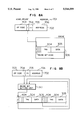
- FIGS. 1A and 1B are a schematic diagram showing the structure of a two-way set associative cache and a table explaining the operation of selecting an entry to be replaced, according to an embodiment of the present invention
- FIG. 2 is a schematic diagram showing an information processing computer system to which the present invention is applied;
- FIG. 3 shows the structure of a cache according to an embodiment of the invention
- FIG. 4 is a schematic diagram showing one line of the cache shown in FIG. 3;
- FIG. 5 shows the structure of a memory address according to an embodiment of the invention
- FIG. 6 is a schematic diagram explaining the operation of a cache access according to an embodiment of the invention.
- FIG. 7 is a flow chart explaining the operation of a cache control method, including processes from a memory access request to a replacement of data in an entry, according to an embodiment of the invention
- FIGS. 8A and 8B are schematic diagrams explaining the format of a load instruction from CPU and a method of setting reuse information to a cache entry, according to an embodiment of the invention
- FIG. 9 shows an example of a program involving accesses to a cache, with reference to which a cache operation will be described;
- FIG. 10 shows the program of FIG. 9 expressed in machine language like form, the program being used for explaining a conventional cache operation
- FIG. 11 shows the program of FIG. 9 expressed in machine language like form, the program being used for explaining a cache operation of the invention.
- FIG. 2 is a schematic block diagram of an information processing system with a cache according to the present invention.
- a cache 202 is a memory having a small capacity and a high access speed
- a main memory 202 (hereinafter simply called a memory) is a memory having a large capacity and a low access speed.
- the cache and memory are both connected to a bus 203, and a CPU 201 is connected via the cache 202 to the bus 203.
- CPU accesses data in the cache 202 if it is present in the cache 202, or accesses data in the memory 204 if it is not present in the cache 202.
- a conventional cache is also configured as shown in FIG. 2.
- FIG. 3 shows the structure of a cache according to an embodiment of the invention.
- This cache is a two-way set associative cache (having a first set 301 and a second set 302).
- the capacity of the cache is 8 Kbyte in total, each set having a capacity of 4 Kbyte.
- Data is stored in the cache in the form of an array and in the unit of a line.
- Each set has 128 lines (entries) 306 from the 0-th to 127-th lines.
- the number of each line is called an index 307.
- One entry can store eight words assuming that one word is constituted by four bytes.
- One line has three fields including a control bit field 303, a tag field 304, and a data field 305. These fields will be explained with reference to FIG. 4.
- FIG. 4 shows the structure of one line of the cache of the present invention.
- a line 306 has a control information area for storing control information and a data area for storing data.
- the control information includes "empty" information, "recent” information, "dirty” information, and "reuse” information.
- each information is one-bit information.
- the control information area stores control bits 303.
- the data area has a tag field 304 and a data field 305.
- the control bits include an empty bit 401, a recent bit 402, a dirty bit 403, and a reuse bit 404.
- the data field loads the values of data stored in the memory.
- the tag field identifies what memory address the loaded data has.
- the empty bit indicates whether the corresponding line is empty or not (true is empty).
- the recent bit indicates whether the corresponding line of the set has been accessed later than the corresponding line of the other set, i.e., indicates whether the line has been accessed most recently (true is recent).
- the recent bit is required because the cache uses an LRU replacement rule.
- the dirty bit indicates whether the corresponding line has been rewritten or not (true is rewrite).
- the reuse bit indicates whether the data in the corresponding line has a high possibility of being reused in the future. This bit is set by an instruction of referring to the corresponding memory address, and referred when a cache data replacement becomes necessary. This will be detailed later.
- FIG. 5 is a schematic diagram showing the structure of a memory address given by binary representation.
- a memory address has 32 bits including three fields of a tag field 501, an index field 502, and a position field 503.
- the tag field has 20 bits and corresponds to the tag field 304 of a cache line.
- CPU issues a memory access request.
- an entry of a cache line array is identified by using the index value 502 of the memory address 602. Since this cache is a two-way set associative cache, one index identifies two entries (including the entry 603 of the first set and the entry 604 of the second set).
- a comparator 601 compares the tag value 501 of the memory address with the tag values 605 and 606 of the identified entries. If the tag value coincides each other, it is judged that a copy of the memory location contents (data at main memory address) has been stored in one of the two cache entries.
- Step 14 if the tag value 501 of the memory address is coincide with one of the tag values 605 and 606 of the cache entries, a cache hit occurs at Step 14. In this case, the memory access is passed to a cache access, allowing a high speed access.
- the data to be read from the memory is loaded in the cache in the following manner.
- the empty control bits of the two entries of the two sets are checked at Step 17. If there is a true entry bit among the two empty bits of the two entries of the two sets, the data read from the memory is loaded in this empty cache entry at Step 19.
- FIGS. 1A and 1B are a schematic diagram and a table explaining this selection.
- FIGS. 1A and 1B explains how one of the first and second entries 603 and 604 of the two sets is replaced at Step 21.
- the first entry 603 belongs to the first set, and the second entry 604 belongs to the second set.
- the reuse bits and recent bits of the control bits of the two entries of the two sets are supplied to a replacement entry selection unit 101 to select an entry to be replaced.
- the selection unit 101 Upon reception of the four bits, the selection unit 101 outputs "0" or "1". "0" stands for the first entry and "1" stands for the second entry.
- the relationship between the inputs and outputs of the selection unit 101 is shown in the table 102 of FIG. 1B.
- the meanings of this table are as follows.
- both the reuse bits of both the sets are true ("1") or false (“0"), an older entry (having a false recent bit) is selected.
- both the recent bits of the two sets are false (“0").
- one of the sets becomes true (“1") and the other becomes false (“0"), by all means, and both the sets will not become true.
- both the recent bits are false, any one of the sets can be selected (in this table, this is indicated by 0/1).
- the entry to be replaced After the entry to be replaced has been selected, it is checked whether the entry contents have been changed or not (whether the dirty bit is true or not). If the entry contents have been changed, the contents are written in the memory. If not (false dirty bit), the entry contents are not written in the memory.
- reuse bit information 704 of a CPU load instruction is set to the reuse bit information storage field 404 of the entry.
- FIG. 8A is a schematic diagram showing a load instruction and explaining the operation of setting a reuse bit to a cache entry.
- the format 702 of the load instruction contains a bit 704 indicating a reuse designation. If this bit is true, the reuse bit 404 of the cache entry 306 having data accessed by the load instruction is set to true.
- FIG. 8B is a schematic diagram showing an embodiment wherein there is provided a reuse bit setting unit 310 for selecting one of the two entries under the above-described state.
- the control bits of a cache line of a conventional cache system include an empty bit, a recent bit, and a dirty bit.
- an entry having a false recent bit, i.e., an entry accessed earlier, in the cache is replaced.
- the first iteration (repetition unit, each loop of, for example, 99 loops is called an iteration) of an outer loop 802 has been completed.
- the accessed elements in the arrays a and b are a[0 . . . 1] [1 . . . 1023], and b[1 . . . 1023] where b[1 . . . 1023] for example is b[1], b[2], . . . , b[1023].
- the access position of the array a changes with the advancement of iteration of the outer loop, whereas the access position of the array b does not change at the outer loop (or strictly speaking, the total capacity of the array b is smaller than the size of the cache).
- the array b [1 . . . 1023] can be loaded in the cache for a long time and reused by each iteration of the outer loop, the load process can be speeded up efficiently.
- the array b cannot always be loaded in the cache.
- the reason for this is that a cache line contends among the element b[j] of the array b, the element a[1] [j] and element a[i+1] [j] of the array a. This will be clarified in the following.
- the second dimension (j) is disposed in the memory so as to change faster than the first dimension.
- a cache line (index) to which data in the memory at a certain address is loaded is determined by the middle seven bits. If two array elements have the same seven middle bits of their memory addresses, these elements are required to be loaded in the same line (cache line contention). In the case of the two-way set associative cache, there are two entries per one index.
- the address of the element b[j] is "the start address (address of b[0]) of the array b+j * 4"
- the address of the element a[i] [j] is "the start address (address of a[0] [0]) of the array a+i*4096 +j*4". Therefore, the addresses of a[i] [j] and a[i+1] [j] have a difference of 4096, and the two elements are required to be loaded in the same cache line.
- FIG. 10 shows the program of FIG. 9 expressed in machine language like form.
- the access to the subject arrays a and b are explicitly written by load ().
- r0, r1, and r2 represent a register.
- the array elements are accessed in the order of a[i] [j], a[i+1] [j], and b[j].
- an element a[2] [J] is first accessed.
- the elements a[1] [J] and b[J] remain in the corresponding entries.
- this element in the cache is replaced by the element a[2] [J].
- the recent bit of the remaining element b[J] is set to false, whereas the recent bit of the new element a[2] [J] is set to true.
- an element a[3] [J] is accessed, and the element b[J] is replaced by the element a[3] [J].
- an element b[J] is accessed, and the element a[2] [J] in the cache is replaced by the element b[J].
- the element b[J] is once replaced and then newly fetched from the memory. That is to say, at an arbitrary iteration of the outer loop (i is an arbitrary value, and j is an arbitrary value J), the element b[J] is fetched from the memory. This means that the whole array b does not remain in the cache because the value j is arbitrary.
- FIG. 11 shows the program of FIG. 9 expressed in machine language like form.
- the memory access is explicitly written by load () having a designation of reuse.
- the execution of the program of FIG. 11 will be explained by using the cache of the invention.
- the iteration of the inner loop is fixed (j is a fixed value of J) and the iteration of the outer loop is sequentially increased.
- the recent bit of the element b[J] is set to true (the recent bit of the element a[1] [J] is false).
- An access to the element b[J] designates a reuse 1006 so that the reuse bit of the element b[J] is also set to true.
- an access to three array elements a[2] [J], a[3] [J], and b[J] is performed.
- An element a[2] [J] is first accessed, and the element a[1] [J] in the cache is replaced by the element a[2] [J] because both the reuse and recent bits of the element a[1] [J] are false.
- the element a[3] [J] is accessed, and either the elements a[2] [J] or b[J] in the cache are replaced.
- the element a[2] [J] has a false reuse bit and a true recent bit
- the element b[J] has a true reuse bit and a false recent bit. Therefore, as shown in FIG. 1B, the entry of the element a[2] [J] is selected to be replaced, and the element b[J] remains in the cache.
- the element a[3] [J] is thereafter loaded in the cache.
- the element b[J] is accessed.
- the element b[J] is present in the cache (cache hit) so that it is not necessary to access the memory, but this element is accessed from the cache.
- the element b[J] has a true recent bit and a true reuse bit.
- the third and following iterations of the outer loop are generally the same as the second iteration.
- the element a[5] [J] is accessed, and one of the elements a[4] [J] and b[J] in the cache is replaced. Because the element a[4] [J] has a true recent bit and the element b[J] has a true reuse bit, the element a[4] [J] is replaced by the element a[5] [J].
- the element b[J] is accessed.
- the element b[J] is already present in the cache (cache hit).
- the element b[J] is not fetched from the memory if it is once loaded in the cache. That is to say, once the whole array b is fetched from the memory and loaded in the cache at the first iteration of the outer loop, no fetch occurs thereafter. In other words, an access to the array b makes efficient use of time locality, which is the advantageous feature of this invention.
- each entry of the cache has reuse information instructing that data in the entry of the cache is not displaced as much as possible. Accordingly, in determining which entry of the cache is replaced, the reuse information can be used so that the entry having the reuse information can be preferentially remained in the cache.
- the data as well as the reuse designation are set to the entry. Accordingly, a user or compiler can instruct to remain particular data in the cache as much as possible.
Abstract
Description
______________________________________
         float a[1000];
         for (i = 0; i < 100: i + +) {
          . . . a[i * 10] . . .
         }
______________________________________
______________________________________
         float a[100], b[1000] [100];
         for (i = 0; i < 1000; i + +) {
          for (j = 0; j < 100: j + +) {
           . . . a[j] . . .
           . . . b[i] [j] . . .
          }
         }
______________________________________
Claims (9)
Applications Claiming Priority (2)
| Application Number | Priority Date | Filing Date | Title |
|---|---|---|---|
| JP5163148A JPH06348595A (en) | 1993-06-07 | 1993-06-07 | Cache device |
| JP5-163148 | 1993-06-07 |
Publications (1)
| Publication Number | Publication Date |
|---|---|
| US5546559A true US5546559A (en) | 1996-08-13 |
Family
ID=15768137
Family Applications (1)
| Application Number | Title | Priority Date | Filing Date |
|---|---|---|---|
| US08/252,413 Expired - Lifetime US5546559A (en) | 1993-06-07 | 1994-06-01 | Cache reuse control system having reuse information field in each cache entry to indicate whether data in the particular entry has higher or lower probability of reuse |
Country Status (3)
| Country | Link |
|---|---|
| US (1) | US5546559A (en) |
| JP (1) | JPH06348595A (en) |
| KR (1) | KR970000838B1 (en) |
Cited By (36)
| Publication number | Priority date | Publication date | Assignee | Title |
|---|---|---|---|---|
| US5940621A (en) * | 1996-01-23 | 1999-08-17 | Hewlett-Packard Company | Language independent optimal size-based storage allocation |
| US5943687A (en) * | 1997-03-14 | 1999-08-24 | Telefonakiebolaget Lm Ericsson | Penalty-based cache storage and replacement techniques |
| US5974507A (en) * | 1997-04-14 | 1999-10-26 | International Business Machines Corporation | Optimizing a cache eviction mechanism by selectively introducing different levels of randomness into a replacement algorithm |
| WO2000004452A1 (en) * | 1998-07-16 | 2000-01-27 | Intel Corporation | Method and apparatus for managing temporal and non-temporal data in a single cache structure |
| EP1066566A1 (en) * | 1998-03-31 | 2001-01-10 | Intel Corporation | Shared cache structure for temporal and non-temporal instructions |
| WO2001004746A1 (en) * | 1999-07-13 | 2001-01-18 | Coppe/Ufrj - Coordenação Dos Programas De Pós Graduação De Engenharia Da Universidade Federal Do Rio De Janeiro | Process of formation, memorization and reuse, in execution time, of sequences of dynamic instructions in computers |
| US6209062B1 (en) | 1997-11-24 | 2001-03-27 | Intel Corporation | Method for holding cache pages that are not invalidated within normal time duration for a second access or that are likely to be accessed again soon |
| US6266742B1 (en) * | 1997-10-27 | 2001-07-24 | International Business Machines Corporation | Algorithm for cache replacement |
| US6282613B1 (en) | 1999-04-30 | 2001-08-28 | International Business Machines Corporation | Very efficient technique for dynamically tracking locality of a reference |
| US6282706B1 (en) * | 1998-02-10 | 2001-08-28 | Texas Instruments Incorporated | Cache optimization for programming loops |
| US20010032298A1 (en) * | 2000-04-12 | 2001-10-18 | Emons Martijn Johannes Lambertus | Data processing circuit with a cache memory and apparatus containing such a circuit |
| WO2002027498A2 (en) * | 2000-09-29 | 2002-04-04 | Sun Microsystems, Inc. | System and method for identifying and managing streaming-data |
| US20030074525A1 (en) * | 2001-10-17 | 2003-04-17 | Fujitsu Limited | Cache control program and computer for performing cache processes |
| US6578111B1 (en) | 2000-09-29 | 2003-06-10 | Sun Microsystems, Inc. | Cache memory system and method for managing streaming-data |
| US6598124B1 (en) | 2000-09-29 | 2003-07-22 | Sun Microsystems, Inc. | System and method for identifying streaming-data |
| US20030145174A1 (en) * | 2002-01-28 | 2003-07-31 | International Business Machines Corporation | Reducing power in a snooping cache based multiprocessor environment |
| US6640286B2 (en) | 2000-11-02 | 2003-10-28 | Hitachi, Ltd. | Cache control system |
| US6668307B1 (en) | 2000-09-29 | 2003-12-23 | Sun Microsystems, Inc. | System and method for a software controlled cache |
| US20040165608A1 (en) * | 2003-02-24 | 2004-08-26 | Mosaid Technologies Incorporated | Method and apparatus for performing repeated content addressable memory searches |
| US6807607B1 (en) * | 1999-08-17 | 2004-10-19 | International Business Machines Corporation | Cache memory management system and method |
| EP1667028A1 (en) * | 2003-09-19 | 2006-06-07 | Matsushita Electric Industrial Co., Ltd. | Cache memory and cache memory control method |
| US20060224639A1 (en) * | 2005-03-29 | 2006-10-05 | Satoru Watanabe | Backup system, program and backup method |
| US20060224830A1 (en) * | 2005-03-30 | 2006-10-05 | Ibm Corporation | Performance of a cache by detecting cache lines that have been reused |
| US20070186048A1 (en) * | 2004-03-24 | 2007-08-09 | Matsushita Electric Industrial Co., Ltd. | Cache memory and control method thereof |
| KR100801814B1 (en) * | 2003-11-18 | 2008-02-11 | 마쯔시다덴기산교 가부시키가이샤 | Cache memory and control method thereof |
| US20100005241A1 (en) * | 2008-04-08 | 2010-01-07 | Changkyu Kim | Detection of streaming data in cache |
| GB2465474A (en) * | 2008-11-21 | 2010-05-26 | Nvidia Corp | System for evicting or clearing data from a cache based on the eviction class tag of the data stored in the cache. |
| US8131931B1 (en) | 2008-10-22 | 2012-03-06 | Nvidia Corporation | Configurable cache occupancy policy |
| US20120072656A1 (en) * | 2010-06-11 | 2012-03-22 | Shrikar Archak | Multi-tier caching |
| CN104395892B (en) * | 2012-06-27 | 2018-02-13 | 阿尔卡特朗讯公司 | The method that the storage of the list of N items is managed in the memory buffers device of the C items of caching system |
| US10366015B2 (en) * | 2016-06-13 | 2019-07-30 | Fujitsu Limited | Storage medium storing cache miss estimation program, cache miss estimation method, and information processing apparatus |
| US10606752B2 (en) | 2017-11-06 | 2020-03-31 | Samsung Electronics Co., Ltd. | Coordinated cache management policy for an exclusive cache hierarchy |
| US20200117607A1 (en) * | 2018-10-15 | 2020-04-16 | International Business Machines Corporation | Cache line replacement using reference states based on data reference attributes |
| US11113207B2 (en) * | 2018-12-26 | 2021-09-07 | Samsung Electronics Co., Ltd. | Bypass predictor for an exclusive last-level cache |
| US11157286B2 (en) * | 2018-05-07 | 2021-10-26 | Micron Technology, Inc. | Non-cached loads and stores in a system having a multi-threaded, self-scheduling processor |
| US20210374064A1 (en) * | 2018-12-26 | 2021-12-02 | Samsung Electronics Co., Ltd. | Bypass predictor for an exclusive last-level cache |
Families Citing this family (1)
| Publication number | Priority date | Publication date | Assignee | Title |
|---|---|---|---|---|
| WO2012090239A1 (en) * | 2010-12-27 | 2012-07-05 | Hitachi, Ltd. | Storage system and management method of control information therein |
Citations (10)
| Publication number | Priority date | Publication date | Assignee | Title |
|---|---|---|---|---|
| US4513367A (en) * | 1981-03-23 | 1985-04-23 | International Business Machines Corporation | Cache locking controls in a multiprocessor |
| US4680730A (en) * | 1983-07-08 | 1987-07-14 | Hitachi, Ltd. | Storage control apparatus |
| US4914582A (en) * | 1986-06-27 | 1990-04-03 | Hewlett-Packard Company | Cache tag lookaside |
| JPH0358252A (en) * | 1989-07-27 | 1991-03-13 | Nec Corp | Cache memory controller |
| US5043885A (en) * | 1989-08-08 | 1991-08-27 | International Business Machines Corporation | Data cache using dynamic frequency based replacement and boundary criteria |
| US5313609A (en) * | 1991-05-23 | 1994-05-17 | International Business Machines Corporation | Optimum write-back strategy for directory-based cache coherence protocols |
| US5325509A (en) * | 1991-03-05 | 1994-06-28 | Zitel Corporation | Method of operating a cache memory including determining desirability of cache ahead or cache behind based on a number of available I/O operations |
| US5357618A (en) * | 1991-04-15 | 1994-10-18 | International Business Machines Corporation | Cache prefetch and bypass using stride registers |
| US5406504A (en) * | 1993-06-30 | 1995-04-11 | Digital Equipment | Multiprocessor cache examiner and coherency checker |
| US5432918A (en) * | 1990-06-29 | 1995-07-11 | Digital Equipment Corporation | Method and apparatus for ordering read and write operations using conflict bits in a write queue |
-
1993
- 1993-06-07 JP JP5163148A patent/JPH06348595A/en active Pending
-
1994
- 1994-06-01 US US08/252,413 patent/US5546559A/en not_active Expired - Lifetime
- 1994-06-04 KR KR94012632A patent/KR970000838B1/en not_active IP Right Cessation
Patent Citations (10)
| Publication number | Priority date | Publication date | Assignee | Title |
|---|---|---|---|---|
| US4513367A (en) * | 1981-03-23 | 1985-04-23 | International Business Machines Corporation | Cache locking controls in a multiprocessor |
| US4680730A (en) * | 1983-07-08 | 1987-07-14 | Hitachi, Ltd. | Storage control apparatus |
| US4914582A (en) * | 1986-06-27 | 1990-04-03 | Hewlett-Packard Company | Cache tag lookaside |
| JPH0358252A (en) * | 1989-07-27 | 1991-03-13 | Nec Corp | Cache memory controller |
| US5043885A (en) * | 1989-08-08 | 1991-08-27 | International Business Machines Corporation | Data cache using dynamic frequency based replacement and boundary criteria |
| US5432918A (en) * | 1990-06-29 | 1995-07-11 | Digital Equipment Corporation | Method and apparatus for ordering read and write operations using conflict bits in a write queue |
| US5325509A (en) * | 1991-03-05 | 1994-06-28 | Zitel Corporation | Method of operating a cache memory including determining desirability of cache ahead or cache behind based on a number of available I/O operations |
| US5357618A (en) * | 1991-04-15 | 1994-10-18 | International Business Machines Corporation | Cache prefetch and bypass using stride registers |
| US5313609A (en) * | 1991-05-23 | 1994-05-17 | International Business Machines Corporation | Optimum write-back strategy for directory-based cache coherence protocols |
| US5406504A (en) * | 1993-06-30 | 1995-04-11 | Digital Equipment | Multiprocessor cache examiner and coherency checker |
Non-Patent Citations (4)
| Title |
|---|
| Information Processing, vol. 33, No. 11, 1992, pp. 1348 1357 (Japanese). * |
| Information Processing, vol. 33, No. 11, 1992, pp. 1348-1357 (Japanese). |
| Lee, King. "On the Floating Point Performance of the i860™ Microprocessor," International Journal of High Speed Computing, vol. 4, No. 4, 1992, pp. 251-267. (English). |
| Lee, King. On the Floating Point Performance of the i860 Microprocessor, International Journal of High Speed Computing, vol. 4, No. 4, 1992, pp. 251 267. (English). * |
Cited By (63)
| Publication number | Priority date | Publication date | Assignee | Title |
|---|---|---|---|---|
| US5940621A (en) * | 1996-01-23 | 1999-08-17 | Hewlett-Packard Company | Language independent optimal size-based storage allocation |
| US5943687A (en) * | 1997-03-14 | 1999-08-24 | Telefonakiebolaget Lm Ericsson | Penalty-based cache storage and replacement techniques |
| US5974507A (en) * | 1997-04-14 | 1999-10-26 | International Business Machines Corporation | Optimizing a cache eviction mechanism by selectively introducing different levels of randomness into a replacement algorithm |
| US6266742B1 (en) * | 1997-10-27 | 2001-07-24 | International Business Machines Corporation | Algorithm for cache replacement |
| US6209062B1 (en) | 1997-11-24 | 2001-03-27 | Intel Corporation | Method for holding cache pages that are not invalidated within normal time duration for a second access or that are likely to be accessed again soon |
| US6282706B1 (en) * | 1998-02-10 | 2001-08-28 | Texas Instruments Incorporated | Cache optimization for programming loops |
| EP1066566A1 (en) * | 1998-03-31 | 2001-01-10 | Intel Corporation | Shared cache structure for temporal and non-temporal instructions |
| EP1066566A4 (en) * | 1998-03-31 | 2002-10-23 | Intel Corp | Shared cache structure for temporal and non-temporal instructions |
| US6542966B1 (en) * | 1998-07-16 | 2003-04-01 | Intel Corporation | Method and apparatus for managing temporal and non-temporal data in a single cache structure |
| WO2000004452A1 (en) * | 1998-07-16 | 2000-01-27 | Intel Corporation | Method and apparatus for managing temporal and non-temporal data in a single cache structure |
| US6282613B1 (en) | 1999-04-30 | 2001-08-28 | International Business Machines Corporation | Very efficient technique for dynamically tracking locality of a reference |
| WO2001004746A1 (en) * | 1999-07-13 | 2001-01-18 | Coppe/Ufrj - Coordenação Dos Programas De Pós Graduação De Engenharia Da Universidade Federal Do Rio De Janeiro | Process of formation, memorization and reuse, in execution time, of sequences of dynamic instructions in computers |
| US6807607B1 (en) * | 1999-08-17 | 2004-10-19 | International Business Machines Corporation | Cache memory management system and method |
| US20010032298A1 (en) * | 2000-04-12 | 2001-10-18 | Emons Martijn Johannes Lambertus | Data processing circuit with a cache memory and apparatus containing such a circuit |
| US7076612B2 (en) * | 2000-04-12 | 2006-07-11 | Koninklijke Philips Electronics N.V. | Cache interface circuit for automatic control of cache bypass modes and associated power savings |
| US6668307B1 (en) | 2000-09-29 | 2003-12-23 | Sun Microsystems, Inc. | System and method for a software controlled cache |
| WO2002027498A2 (en) * | 2000-09-29 | 2002-04-04 | Sun Microsystems, Inc. | System and method for identifying and managing streaming-data |
| WO2002027498A3 (en) * | 2000-09-29 | 2003-01-23 | Sun Microsystems Inc | System and method for identifying and managing streaming-data |
| US6578111B1 (en) | 2000-09-29 | 2003-06-10 | Sun Microsystems, Inc. | Cache memory system and method for managing streaming-data |
| US6598124B1 (en) | 2000-09-29 | 2003-07-22 | Sun Microsystems, Inc. | System and method for identifying streaming-data |
| US6640286B2 (en) | 2000-11-02 | 2003-10-28 | Hitachi, Ltd. | Cache control system |
| US6842824B2 (en) * | 2001-10-17 | 2005-01-11 | Fujitsu Limited | Cache control program and computer for performing cache processes utilizing cache blocks ranked according to their order of reuse |
| US20030074525A1 (en) * | 2001-10-17 | 2003-04-17 | Fujitsu Limited | Cache control program and computer for performing cache processes |
| US20030145174A1 (en) * | 2002-01-28 | 2003-07-31 | International Business Machines Corporation | Reducing power in a snooping cache based multiprocessor environment |
| US6826656B2 (en) * | 2002-01-28 | 2004-11-30 | International Business Machines Corporation | Reducing power in a snooping cache based multiprocessor environment |
| US20040165608A1 (en) * | 2003-02-24 | 2004-08-26 | Mosaid Technologies Incorporated | Method and apparatus for performing repeated content addressable memory searches |
| US7353330B2 (en) * | 2003-02-24 | 2008-04-01 | Mosaid Technologies Incorporated | Method and apparatus for performing repeated content addressable memory searches |
| EP1667028A1 (en) * | 2003-09-19 | 2006-06-07 | Matsushita Electric Industrial Co., Ltd. | Cache memory and cache memory control method |
| EP1667028A4 (en) * | 2003-09-19 | 2008-10-29 | Matsushita Electric Ind Co Ltd | Cache memory and cache memory control method |
| US20070028055A1 (en) * | 2003-09-19 | 2007-02-01 | Matsushita Electric Industrial Co., Ltd | Cache memory and cache memory control method |
| KR100801814B1 (en) * | 2003-11-18 | 2008-02-11 | 마쯔시다덴기산교 가부시키가이샤 | Cache memory and control method thereof |
| CN100424658C (en) * | 2003-11-18 | 2008-10-08 | 松下电器产业株式会社 | Cache memory and control method thereof |
| US20110179227A1 (en) * | 2003-11-18 | 2011-07-21 | Panasonic Corporation | Cache memory and method for cache entry replacement based on modified access order |
| US7984243B2 (en) | 2003-11-18 | 2011-07-19 | Panasonic Corporation | Cache memory and method for cache entry replacement based on modified access order |
| US20080168232A1 (en) * | 2003-11-18 | 2008-07-10 | Hazuki Okabayashi | Cache Memory and Control Method Thereof |
| US20070186048A1 (en) * | 2004-03-24 | 2007-08-09 | Matsushita Electric Industrial Co., Ltd. | Cache memory and control method thereof |
| US20060224639A1 (en) * | 2005-03-29 | 2006-10-05 | Satoru Watanabe | Backup system, program and backup method |
| US7640276B2 (en) * | 2005-03-29 | 2009-12-29 | Hitachi, Ltd. | Backup system, program and backup method |
| US7552286B2 (en) | 2005-03-30 | 2009-06-23 | International Business Machines Corporation | Performance of a cache by detecting cache lines that have been reused |
| US7380065B2 (en) | 2005-03-30 | 2008-05-27 | International Business Machines Corporation | Performance of a cache by detecting cache lines that have been reused |
| US20060224830A1 (en) * | 2005-03-30 | 2006-10-05 | Ibm Corporation | Performance of a cache by detecting cache lines that have been reused |
| US20100005241A1 (en) * | 2008-04-08 | 2010-01-07 | Changkyu Kim | Detection of streaming data in cache |
| US8667221B2 (en) * | 2008-04-08 | 2014-03-04 | Intel Corporation | Detection of streaming data in cache |
| US8131931B1 (en) | 2008-10-22 | 2012-03-06 | Nvidia Corporation | Configurable cache occupancy policy |
| US8868838B1 (en) * | 2008-11-21 | 2014-10-21 | Nvidia Corporation | Multi-class data cache policies |
| GB2465474B (en) * | 2008-11-21 | 2011-08-31 | Nvidia Corp | Multi-class data cache policies |
| GB2465474A (en) * | 2008-11-21 | 2010-05-26 | Nvidia Corp | System for evicting or clearing data from a cache based on the eviction class tag of the data stored in the cache. |
| US20120072656A1 (en) * | 2010-06-11 | 2012-03-22 | Shrikar Archak | Multi-tier caching |
| US9355109B2 (en) * | 2010-06-11 | 2016-05-31 | The Research Foundation For The State University Of New York | Multi-tier caching |
| US20160232169A1 (en) * | 2010-06-11 | 2016-08-11 | The Research Foundation For The State University Of New York | Multi-tier caching |
| US9959279B2 (en) * | 2010-06-11 | 2018-05-01 | The Research Foundation For The State University Of New York | Multi-tier caching |
| CN104395892B (en) * | 2012-06-27 | 2018-02-13 | 阿尔卡特朗讯公司 | The method that the storage of the list of N items is managed in the memory buffers device of the C items of caching system |
| US10366015B2 (en) * | 2016-06-13 | 2019-07-30 | Fujitsu Limited | Storage medium storing cache miss estimation program, cache miss estimation method, and information processing apparatus |
| US10606752B2 (en) | 2017-11-06 | 2020-03-31 | Samsung Electronics Co., Ltd. | Coordinated cache management policy for an exclusive cache hierarchy |
| US11157286B2 (en) * | 2018-05-07 | 2021-10-26 | Micron Technology, Inc. | Non-cached loads and stores in a system having a multi-threaded, self-scheduling processor |
| US20220004389A1 (en) * | 2018-05-07 | 2022-01-06 | Micron Technology, Inc. | Non-Cached Loads and Stores in a System Having a Multi-Threaded, Self-Scheduling Processor |
| US11579888B2 (en) * | 2018-05-07 | 2023-02-14 | Micron Technology, Inc. | Non-cached loads and stores in a system having a multi-threaded, self-scheduling processor |
| US20200117607A1 (en) * | 2018-10-15 | 2020-04-16 | International Business Machines Corporation | Cache line replacement using reference states based on data reference attributes |
| US10671539B2 (en) * | 2018-10-15 | 2020-06-02 | International Business Machines Corporation | Cache line replacement using reference states based on data reference attributes |
| US10776275B2 (en) | 2018-10-15 | 2020-09-15 | International Business Machines Corporation | Cache data replacement in a networked computing system using reference states based on reference attributes |
| US11113207B2 (en) * | 2018-12-26 | 2021-09-07 | Samsung Electronics Co., Ltd. | Bypass predictor for an exclusive last-level cache |
| US20210374064A1 (en) * | 2018-12-26 | 2021-12-02 | Samsung Electronics Co., Ltd. | Bypass predictor for an exclusive last-level cache |
| US11609858B2 (en) * | 2018-12-26 | 2023-03-21 | Samsung Electronics Co., Ltd. | Bypass predictor for an exclusive last-level cache |
Also Published As
| Publication number | Publication date |
|---|---|
| JPH06348595A (en) | 1994-12-22 |
| KR970000838B1 (en) | 1997-01-20 |
Similar Documents
| Publication | Publication Date | Title |
|---|---|---|
| US5546559A (en) | Cache reuse control system having reuse information field in each cache entry to indicate whether data in the particular entry has higher or lower probability of reuse | |
| US6226715B1 (en) | Data processing circuit with cache memory and cache management unit for arranging selected storage location in the cache memory for reuse dependent on a position of particular address relative to current address | |
| US6381679B1 (en) | Information processing system with prefetch instructions having indicator bits specifying cache levels for prefetching | |
| US5535361A (en) | Cache block replacement scheme based on directory control bit set/reset and hit/miss basis in a multiheading multiprocessor environment | |
| US5555392A (en) | Method and apparatus for a line based non-blocking data cache | |
| US5568626A (en) | Method and system for rewriting data in a non-volatile memory a predetermined large number of times | |
| US6782454B1 (en) | System and method for pre-fetching for pointer linked data structures | |
| US4914582A (en) | Cache tag lookaside | |
| WO1998027486A1 (en) | Method and apparatus for storing and expanding programs for vliw processor architectures | |
| US20040143708A1 (en) | Cache replacement policy to mitigate pollution in multicore processors | |
| US5619696A (en) | Program cache apparatus which associates the physical address of a physical page with both the logical address in a program cache space and the logical address in a process space | |
| US3949368A (en) | Automatic data priority technique | |
| US6065099A (en) | System and method for updating the data stored in a cache memory attached to an input/output system | |
| US20050240731A1 (en) | Managing a multi-way associative cache | |
| US6687807B1 (en) | Method for apparatus for prefetching linked data structures | |
| US7406579B2 (en) | Selectively changeable line width memory | |
| US5729711A (en) | Data driven information processing system using address translation table to keep coherent cache and main memories and permitting parallel readings and writings | |
| US7219197B2 (en) | Cache memory, processor and cache control method | |
| US6785770B2 (en) | Data processing apparatus with a cache memory and method of using such an apparatus | |
| US6862663B1 (en) | Cache having a prioritized replacement technique and method therefor | |
| CA1279731C (en) | Cache memory with variable fetch and replacement schemes | |
| US5535360A (en) | Digital computer system having an improved direct-mapped cache controller (with flag modification) for a CPU with address pipelining and method therefor | |
| CN115168248B (en) | Cache memory supporting SIMT architecture and corresponding processor | |
| JP4741844B2 (en) | Memory that can selectively change the line width | |
| US20030196024A1 (en) | Apparatus and method for a skip-list based cache |
Legal Events
| Date | Code | Title | Description |
|---|---|---|---|
| AS | Assignment |
Owner name: HITACHI, LTD., JAPAN Free format text: ASSIGNMENT OF ASSIGNORS INTEREST;ASSIGNORS:KYUSHIMA, ICHIRO;KAINAGA, MASAHIRO;REEL/FRAME:007024/0178 Effective date: 19940527 |
|
| STCF | Information on status: patent grant |
Free format text: PATENTED CASE |
|
| FEPP | Fee payment procedure |
Free format text: PAYOR NUMBER ASSIGNED (ORIGINAL EVENT CODE: ASPN); ENTITY STATUS OF PATENT OWNER: LARGE ENTITY |
|
| FPAY | Fee payment |
Year of fee payment: 4 |
|
| FPAY | Fee payment |
Year of fee payment: 8 |
|
| FEPP | Fee payment procedure |
Free format text: PAYER NUMBER DE-ASSIGNED (ORIGINAL EVENT CODE: RMPN); ENTITY STATUS OF PATENT OWNER: LARGE ENTITY |
|
| FEPP | Fee payment procedure |
Free format text: PAYOR NUMBER ASSIGNED (ORIGINAL EVENT CODE: ASPN); ENTITY STATUS OF PATENT OWNER: LARGE ENTITY |
|
| FPAY | Fee payment |
Year of fee payment: 12 |
|
| AS | Assignment |
Owner name: RENESAS ELECTRONICS CORPORATION, JAPAN Free format text: ASSIGNMENT OF ASSIGNORS INTEREST;ASSIGNOR:HITACHI, LTD.;REEL/FRAME:026109/0528 Effective date: 20110307 |