US5386547A - System and method for exclusive two-level caching - Google Patents
System and method for exclusive two-level caching Download PDFInfo
- Publication number
- US5386547A US5386547A US07/823,671 US82367192A US5386547A US 5386547 A US5386547 A US 5386547A US 82367192 A US82367192 A US 82367192A US 5386547 A US5386547 A US 5386547A
- Authority
- US
- United States
- Prior art keywords
- cache
- level cache
- level
- data
- instruction
- Prior art date
- Legal status (The legal status is an assumption and is not a legal conclusion. Google has not performed a legal analysis and makes no representation as to the accuracy of the status listed.)
- Expired - Lifetime
Links
Images


Classifications
-
- G—PHYSICS
- G06—COMPUTING; CALCULATING OR COUNTING
- G06F—ELECTRIC DIGITAL DATA PROCESSING
- G06F12/00—Accessing, addressing or allocating within memory systems or architectures
- G06F12/02—Addressing or allocation; Relocation
- G06F12/08—Addressing or allocation; Relocation in hierarchically structured memory systems, e.g. virtual memory systems
- G06F12/0802—Addressing of a memory level in which the access to the desired data or data block requires associative addressing means, e.g. caches
- G06F12/0893—Caches characterised by their organisation or structure
- G06F12/0897—Caches characterised by their organisation or structure with two or more cache hierarchy levels
-
- G—PHYSICS
- G06—COMPUTING; CALCULATING OR COUNTING
- G06F—ELECTRIC DIGITAL DATA PROCESSING
- G06F12/00—Accessing, addressing or allocating within memory systems or architectures
- G06F12/02—Addressing or allocation; Relocation
- G06F12/08—Addressing or allocation; Relocation in hierarchically structured memory systems, e.g. virtual memory systems
- G06F12/0802—Addressing of a memory level in which the access to the desired data or data block requires associative addressing means, e.g. caches
- G06F12/0864—Addressing of a memory level in which the access to the desired data or data block requires associative addressing means, e.g. caches using pseudo-associative means, e.g. set-associative or hashing
Definitions
- the present invention relates generally to a cache memory system and to a method of operating a cache memory system. More particularly, it relates to such a cache memory system and method utilizing a first, small upper level of cache and a second, large lower level of cache. Most especially, it relates to such a cache memory system and method which has the lower latency of a direct-mapped cache on a hit and the lower miss rate of a set-associative cache.
- Direct-mapped caches have higher miss rates than set-associative caches but have lower latency than set-associative caches on a hit. Since hits are much more frequent than misses, direct-mapped caches are preferred. The direct-mapped cache has a lower hit rate than a more associative cache because it will have more misses due to accesses which map to the same line in the cache but have different tags. These are called conflict misses. Conflict misses can account for a significant percentage of direct-mapped cache misses.
- Two-level cache structures typically have copies of at least some of the data in the first level of cache in the second level of cache.
- first-level cache and the second-level cache are direct-mapped, mixed, and have the same line size, in conventional systems every cache line in the first-level cache will also be in the second-level cache.
- a copy of all data in the first level cache must reside in the second level cache. This is called inclusion.
- the present invention is directed to a technique for achieving this easily, especially in a two-level on-chip cache structure.
- a cache memory system in accordance with this invention has a first-level cache configured to store tags and instructions or data associated with the tags and a second-level cache configured to store tags and instructions or data associated with the tags.
- the first-level cache and the second-level cache are connected by swap tag lines, swap data lines and swap/read lines.
- the first level cache is connected to read data and write data lines for connection to a processor.
- the second level cache is connected to write tag and write data lines for connection to a next lower level in a memory hierarchy.
- Read data lines are connected from the next lower level in the memory hierarchy to the first-level cache through the swap/read lines and a first multiplexer between a portion of the swap data lines and the swap/read lines. The multiplexer selects the swap data unless the second-level cache misses, in which case the read data is selected.
- a method of operating a cache memory system in accordance with this invention includes storing tags and instructions or data associated with the tags in a first-level cache and in a second-level cache. Instruction and data addresses are supplied from a processor to the first-level cache to determine if desired instructions or data are present in the first-level cache. Instruction or data addresses are supplied from the processor to the second-level cache to determine if desired instructions or data are present in the second-level cache. An instruction or data is swapped from the second-level cache to the first-level cache when the instruction or data is not present in the first-level cache and is present in the second-level cache.
- the instruction or data is read from a lower level in the memory hierarchy directly to the first-level cache when the instruction or data is present in neither the first-level cache nor the second-level cache. In this case, the former contents of the first-level cache are still transferred to the second-level cache.
- swapping in accordance with the invention can significantly improve the performance of a second-level cache.
- the miss rate of the second-level cache or caches is reduced by 20 percent with swapping.
- a system with swapping has a performance greater than that of a two-way set-associative cache because of its combination of miss rates a lower cache access time on a hit.
- the system with swapping has a significant saving in cycles per instruction.
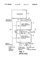
- FIG. 1 is a block diagram of a simple prior art cache memory system.
- FIG. 2 is a block diagram of a comparable cache memory system in accordance with the invention.
- FIGS. 2A and 2B are more detailed block and flow diagrams of a portion of a second embodiment of a cache memory system in accordance with the invention, useful for understanding operation of the invention.
- FIG. 3 is a block diagram of a third embodiment of a cache memory system in accordance with the invention.
- FIG. 4 is a block diagram of a fourth embodiment of a cache memory system in accordance with the invention.
- FIGS. 5-7 are graphs of results obtained with simulations of the invention.
- the system 10 has a first, small upper level cache 12 and a second, large lower level cache 14.
- the cache memory system 10 is mixed because the caches 12 and 14 contain mixed instructions and data.
- the cache 12 is connected to the cache 14 by read and write tag lines 16 and 18 and read and write data lines 20 and 22.
- the level 1 cache 12 is connected to a processor 24 by read and write data lines 26 and 28.
- the level 2 cache 14 is connected to a next lower level in the memory hierarchy by write tag, write data and read data lines 30, 32 and 34.
- the processor 24 is connected to the level 1 cache 12, the level 2 cache 14 and the next lower level in the memory hierarchy by instruction or data address lines 36.
- the processor 24 when the processor 24 requires an instruction or data, it puts out the address for that instruction or data on line 36. If the instruction or data is in the level 1 cache 14, it is supplied directly to the processor 24 from there on read data line 26. If the instruction or data is not present in the level 1 cache, the processor 24 looks for it in the level 2 cache 14. If the instruction or data is found there, it is rippled through the level 1 cache 12 to the processor 24. If the instruction or data is also not present in the level 2 cache 14, the processor looks for it in the next lower level in the memory hierarchy. If it is found there, it is rippled through the level 2 and level 1 caches 14 and 12 to the processor 24.
- Such prior art memory cache systems 10 are operated either as direct-mapped caches or as set-associative caches.
- FIG. 2 shows a simple mixed first level cache memory system 50 of the invention.
- a level 1 cache 52 is connected to a processor 54 by read data and write data lines 56 and 58.
- the level 1 cache 52 is connected to level 2 cache 60 by swap tag lines 62 and 64, swap data lines 66 and 68, multiplexer 70 and swap/read line 72.
- the multiplexer 70 selects swap data line 68 unless the second-level cache misses, in which case read data line 78 is selected.
- the level 2 cache 60 is connected to the next lower level in the memory hierarchy by write tag and write data lines 74 and 76.
- the next lower level in the memory hierarchy below the level 2 cache 60 is also connected by a read data line 78 through the multiplexer 70 and the swap/read line 72 to the level 1 cache 52.
- the processor 54 is connected to the level 1 cache 52, the level 2 cache 60 and to each level in the memory hierarchy below the level 2 cache 60 by instruction or data address lines 80.
- processor 54 In operation of the cache memory system 50, when processor 54 requires an instruction or data, it puts out an address on lines 80. If the instruction or data is present in the level 1 cache 52, it is supplied to the processor 54 on read data line 56. If the instruction or data is not present in the level 1 cache 52, the processor looks for it in the level 2 cache 60 by putting out the address of the instruction or data on lines 80. If the instruction or data is in the level 2 cache, it is supplied to the processor 54 through the level 1 cache 52 by means of a swap operation on tag swap lines 62 and 64, swap data lines 66 and 68, multiplexer 70 and swap/read data line 72.
- the desired instruction or data in the level 2 cache 60 is written into the level 1 cache 52 concurrently with the unwanted data or instruction from the level 1 cache 52 being written to the appropriate location in the level 2 cache 60.
- the desired instruction or data is then read into the processor 54 from the level 1 cache 52. If the instruction or data is present in neither the level 1 cache 52 nor the level 2 cache 60, the address on lines 80 fetches the instruction or data from successively lower levels in the memory hierarchy as required via read data line 78, multiplexer 70 and swap/read data line 72. The instruction or data is then supplied from the level 1 cache to the processor 54.
- mapping conflicts in the first-level cache that do not conflict in the second-level cache do not have exclusion.
- FIG. 2A This system shows an example first-level cache 82 with four lines and a second-level cache 84 with 16 lines.
- the simplest exclusion method requires that the line size of the first and second level caches be the same. It also requires that the write policy of both caches be the same, e.g., write-back or write-through. Simplest implementation methods also require both caches to be physically mapped.
- the exclusion method can also be used in a cache memory system 100 with a first-level cache 102 split into separate instruction and data direct-mapped caches 104 and 106, but with a second-level cache 108 containing both instructions and data, i.e., mixed.
- the level 1 instruction cache 104 is connected to processor 110 by instruction data lines 112.
- the level 1 data cache 106 is connected to the processor 110 by data data lines 114.
- the level 1 cache 102 is connected to the level 2 cache 108 by swap tag lines 114, swap tag lines 109, swap tag lines 111, multiplexer 113, swap tag lines 115, swap data lines 116, swap data lines 121, multiplexer 117, swap data lines 119, swap data lines 118, multiplexer 120 and swap/read data lines 122.
- the next lower level in the memory system hierarchy is connected to the level 1 data cache by read data lines 128, multiplexer 120 and swap/read data lines 122.
- the multiplexer 113 selects instruction tags from level 1 instruction cache 104 or data tags from level 1 data cache 106, as required for swapping with instruction or data tags in the level 2 cache 108.
- the multiplexer 117 selects instructions from level 1 instruction cache 104 or data from level 1 data cache 106, as required for swapping with instructions or data in the level 2 cache 108.
- the multiplexer 120 selects swap data lines 118 unless the second-level cache 108 misses, in which case the multiplexer 120 selects read data lines 128.
- the level 2 cache is also connected to the next lower level in the memory system hierarchy by write address and write data lines 124 and 126.
- the processor 110 is connected to the level 1 instruction cache 104, the level 2 cache 108 and the lower levels of the memory system hierarchy by instruction address lines 130, multiplexer 132 and data address lines 134 and 136. Data address lines 134 are also connected to the level 1 data cache 106.
- multiplexer 132 selects the instruction address 130 during an instruction cache miss, and selects the data address 134 during a data cache miss.
- cache lines will only be transferred to the first level caches 104 and 106 as requested. Thus, dirty data lines will not be loaded into the instruction cache 104 unless actually referenced as instructions, which is an error. Similarly, instruction cache lines will not be placed in the first-level data cache 106 (also not allowed by the virtual memory protection modes).
- the equivalent of three-way set-associativity may be provided for some of the lines in the second-level cache. Of course, this three-way associativity requires at least one instruction and data entry in each set at all times.
- the construction and operation of the FIG. 3 embodiment of the invention is the same as that of the FIG. 2 embodiment.
- the basic configuration and method of the FIG. 3 system can be extended to have virtual instruction caching and physical data cache dam by the addition of a bit per line of the mixed cache. This bit indicates whether the line is instruction or dam, i.e., equivalently whether its address is physical or virtual. Methods with both virtual instruction and dam addressing can also be constructed.
- FIG. 4 shows a cache memory system 150 with a first-level cache 152 split into separate instruction and data direct-mapped caches 154 and 156, and a second-level cache 158, also split into separate instruction and data direct-mapped caches 157 and 159.
- the level 1 instruction cache 154 is connected to processor 160 by read data lines 152.
- the level 1 data cache 156 is connected to the processor 160 by read data lines 153 and write data lines 155.
- the level 1 cache 152 is connected to the level 2 instruction cache 157 by swap tag lines 164, swap data lines 166, swap data lines 168, multiplexer 170 and swap/read data lines 172.
- the next lower level in the memory system hierarchy is connected to the level 1 instruction cache 154 by read data lines 178, multiplexer 170 and swap/read data lines 172.
- the multiplexer 170 selects swap data lines 168 unless the second-level instruction cache 157 misses, in which case the multiplexer 170 selects read data lines 178.
- the level 2 data cache 159 is connected to the level 1 data cache 156 by swap tag lines 179, swap data lines 181, swap data lines 183, multiplexer 185 and swap/read data lines 187.
- the level 2 data cache 159 is also connected to the next lower level in the memory system hierarchy by write tag and write data lines 174 and 176.
- the multiplexer 185 selects swap data lines 183 unless the second-level dam cache 159 misses, in which case the multiplexer 185 selects read data lines 188.
- the processor 160 is connected to the level 1 instruction cache 154, the level 2 instruction cache 157, the level 1 data cache 156, the level 2 data cache 159 and the lower levels of the memory system hierarchy by instruction address lines 180 and data address lines 184.
- the construction and operation of the FIG. 4 embodiment of the invention is the same as that of the FIG. 3 embodiment.
- a more complicated extension to the basic method can allow cache lines of different sizes.
- valid bits must be provided on the granularity of the smallest cache line.
- the excess data is discarded.
- the valid bits in the larger line corresponding to the data not provided from the smaller line must be turned off.
- FIG. 5 shows the reduction in second-level cache miss rate for a system with two 4KB caches and a mixed second level cache of various sizes. This data also assumes 16B lines in both the first-level cache and the second-level cache.
- the miss rate of the second-level cache is reduced by 20% by swapping. As the ratio in cache sizes gets smaller, the benefits of swapping increase.
- a swapping system with second-level cache only as large as each first-level cache can still be useful in some circumstances. In a conventional system, this would not make sense, since all misses in the first-level cache would also miss in the second-level cache if they were the same size.
- FIG. 6 shows the miss rate reduction of a swapping system over a direct-mapped cache relative to a conventional system with a two-way set associative second-level cache. All systems are assumed to use 16B cache lines, and have separate 4KB instruction and data caches. On average, a direct-mapped system with swapping outperforms a system with a two-way set-associative second level cache for ratios of primary to secondary cache sizes of 4:1 or less (i.e., total capacities of 2:1 or less since there are dual 4KB primary caches.) For systems with dual 4 KB primary caches and a 32KB second-level cache, a system with swapping has about the same reduction in miss rate as a two-way set-associative cache.
- the set associative cache has a lower miss rate.
- the performance of the swapping system can still be greater, even at larger ratios, since it has the lower cache access time on a hit of a direct-mapped cache in comparison to the slower access time of a set-associative cache.
- FIG. 7 gives the overall cycles per instruction (CPI) saved by swapping over a conventional direct-mapped cache for 4KB split primary caches, 16B lines, and various second-level cache sizes. These simulations assume a 7 cycle first-level cache miss penalty, and a 20 cycle second-level cache miss penalty. Typically, machines require a total cycles per instruction of 1.5 to 2. Therefore, even with a second-level cache size of 32KB, the savings of almost 0.1 CPI can still be a significant improvement in machine performance.
- CPI cycles per instruction
- tag and data lines 62, 64, 164, 166, 168 and 172 could be replaced with bidirectional lines by using separate operation cycles for transfer in each direction. It is intended that such changes be included within the spirit and scope of the claims appended hereto.
Abstract
Description
______________________________________
program
       dynamic  data    data  total program
name   instr.   reads   writes
                              refs. type
______________________________________
ccom   31.5M     8.3M    5.7M  45.5M
                                    C compiler
grr    134.2M   42.1M   17.1M 193.4M
                                    PC board CAD
                                    tool
yacc   51.0M    12.9M    3.8M  67.7M
                                    Unix utility
met    99.4M    36.4M   13.8M 149.7M
                                    PC board CAD
                                    tool
linpack
       144.8M   28.1M   12.1M 185.5M
                                    numeric, 100 ×
                                    100
liver  23.6M     5.0M    2.3M  31.0M
                                    Livermore loops
                                    1-14
______________________________________
Claims (29)
Priority Applications (1)
| Application Number | Priority Date | Filing Date | Title |
|---|---|---|---|
| US07/823,671 US5386547A (en) | 1992-01-21 | 1992-01-21 | System and method for exclusive two-level caching |
Applications Claiming Priority (1)
| Application Number | Priority Date | Filing Date | Title |
|---|---|---|---|
| US07/823,671 US5386547A (en) | 1992-01-21 | 1992-01-21 | System and method for exclusive two-level caching |
Publications (1)
| Publication Number | Publication Date |
|---|---|
| US5386547A true US5386547A (en) | 1995-01-31 |
Family
ID=25239377
Family Applications (1)
| Application Number | Title | Priority Date | Filing Date |
|---|---|---|---|
| US07/823,671 Expired - Lifetime US5386547A (en) | 1992-01-21 | 1992-01-21 | System and method for exclusive two-level caching |
Country Status (1)
| Country | Link |
|---|---|
| US (1) | US5386547A (en) |
Cited By (86)
| Publication number | Priority date | Publication date | Assignee | Title |
|---|---|---|---|---|
| WO1996010789A1 (en) * | 1994-09-30 | 1996-04-11 | Intel Corporation | Method and apparatus for processing memory-type information within a microprocessor |
| US5537570A (en) * | 1993-10-12 | 1996-07-16 | Texas Instruments Incorporated | Cache with a tag duplicate fault avoidance system and method |
| US5564035A (en) * | 1994-03-23 | 1996-10-08 | Intel Corporation | Exclusive and/or partially inclusive extension cache system and method to minimize swapping therein |
| US5581725A (en) * | 1992-09-30 | 1996-12-03 | Nec Corporation | Cache memory system having first and second direct-mapped cache memories organized in hierarchical structure |
| EP0745941A2 (en) * | 1995-06-02 | 1996-12-04 | Sun Microsystems, Inc. | A system and method for providing a flexible memory hierarchy |
| US5584013A (en) * | 1994-12-09 | 1996-12-10 | International Business Machines Corporation | Hierarchical cache arrangement wherein the replacement of an LRU entry in a second level cache is prevented when the cache entry is the only inclusive entry in the first level cache |
| US5586279A (en) * | 1993-02-03 | 1996-12-17 | Motorola Inc. | Data processing system and method for testing a data processor having a cache memory |
| US5604894A (en) * | 1994-06-15 | 1997-02-18 | Texas Instruments Incorporated | Memory management system for checkpointed logic simulator with increased locality of data |
| US5627990A (en) * | 1994-06-20 | 1997-05-06 | International Business Machines Corporation | Management system for a hierarchical data cache employing preemptive cache track demotion and restaging to adapt to access patterns |
| US5680571A (en) * | 1995-12-28 | 1997-10-21 | Unisys Corporation | Multi-processor data processing system with multiple, separate instruction and operand second level caches |
| US5717890A (en) * | 1991-04-30 | 1998-02-10 | Kabushiki Kaisha Toshiba | Method for processing data by utilizing hierarchical cache memories and processing system with the hierarchiacal cache memories |
| US5721864A (en) * | 1995-09-18 | 1998-02-24 | International Business Machines Corporation | Prefetching instructions between caches |
| US5737751A (en) * | 1996-03-26 | 1998-04-07 | Intellectual Business Machines Corporation | Cache memory management system having reduced reloads to a second level cache for enhanced memory performance in a data processing system |
| US5740399A (en) * | 1995-08-23 | 1998-04-14 | International Business Machines Corporation | Modified L1/L2 cache inclusion for aggressive prefetch |
| US5758119A (en) * | 1995-08-23 | 1998-05-26 | International Business Machines Corp. | System and method for indicating that a processor has prefetched data into a primary cache and not into a secondary cache |
| US5761706A (en) * | 1994-11-01 | 1998-06-02 | Cray Research, Inc. | Stream buffers for high-performance computer memory system |
| US5778422A (en) * | 1996-04-04 | 1998-07-07 | International Business Machines Corporation | Data processing system memory controller that selectively caches data associated with write requests |
| US5778426A (en) * | 1995-10-23 | 1998-07-07 | Symbios, Inc. | Methods and structure to maintain a two level cache in a RAID controller and thereby selecting a preferred posting method |
| US5813028A (en) * | 1993-10-12 | 1998-09-22 | Texas Instruments Incorporated | Cache read miss request invalidation prevention method |
| US5819060A (en) * | 1996-10-08 | 1998-10-06 | Lsi Logic Corporation | Instruction swapping in dual pipeline microprocessor |
| US5826052A (en) * | 1994-04-29 | 1998-10-20 | Advanced Micro Devices, Inc. | Method and apparatus for concurrent access to multiple physical caches |
| US5829024A (en) * | 1992-05-21 | 1998-10-27 | Fujitsu Limited | Hierarchical cache memory system and method for controlling data coherency between a primary and a secondary cache |
| US5829038A (en) * | 1996-06-20 | 1998-10-27 | Intel Corporation | Backward inquiry to lower level caches prior to the eviction of a modified line from a higher level cache in a microprocessor hierarchical cache structure |
| US5835908A (en) * | 1996-11-19 | 1998-11-10 | Microsoft Corporation | Processing multiple database transactions in the same process to reduce process overhead and redundant retrieval from database servers |
| US5860093A (en) * | 1997-01-21 | 1999-01-12 | Unisys Corporation | Reduced instruction processor/storage controller interface |
| US5860095A (en) * | 1996-01-02 | 1999-01-12 | Hewlett-Packard Company | Conflict cache having cache miscounters for a computer memory system |
| US5860100A (en) * | 1996-10-07 | 1999-01-12 | International Business Machines Corporation | Pipelined flushing of a high level cache and invalidation of lower level caches |
| US5875462A (en) * | 1995-12-28 | 1999-02-23 | Unisys Corporation | Multi-processor data processing system with multiple second level caches mapable to all of addressable memory |
| US5875201A (en) * | 1996-12-30 | 1999-02-23 | Unisys Corporation | Second level cache having instruction cache parity error control |
| EP0905628A2 (en) * | 1997-09-30 | 1999-03-31 | Sun Microsystems, Inc. | Reducing cache misses by snarfing writebacks in non-inclusive memory systems |
| US5895487A (en) * | 1996-11-13 | 1999-04-20 | International Business Machines Corporation | Integrated processing and L2 DRAM cache |
| US5903910A (en) * | 1995-11-20 | 1999-05-11 | Advanced Micro Devices, Inc. | Method for transferring data between a pair of caches configured to be accessed from different stages of an instruction processing pipeline |
| US5926830A (en) * | 1996-10-07 | 1999-07-20 | International Business Machines Corporation | Data processing system and method for maintaining coherency between high and low level caches using inclusive states |
| US5940618A (en) * | 1997-09-22 | 1999-08-17 | International Business Machines Corporation | Code instrumentation system with non intrusive means and cache memory optimization for dynamic monitoring of code segments |
| US5943681A (en) * | 1995-07-03 | 1999-08-24 | Mitsubishi Denki Kabushiki Kaisha | Semiconductor memory device having cache function |
| US5960455A (en) * | 1996-12-30 | 1999-09-28 | Unisys Corporation | Scalable cross bar type storage controller |
| US6021471A (en) * | 1994-11-15 | 2000-02-01 | Advanced Micro Devices, Inc. | Multiple level cache control system with address and data pipelines |
| US6065097A (en) * | 1996-08-29 | 2000-05-16 | Sun Microsystems, Inc. | Apparatus and method for sharing a unified memory bus between external cache memory and primary memory |
| US6073212A (en) * | 1997-09-30 | 2000-06-06 | Sun Microsystems, Inc. | Reducing bandwidth and areas needed for non-inclusive memory hierarchy by using dual tags |
| US6128702A (en) * | 1996-07-01 | 2000-10-03 | Sun Microsystems, Inc. | Integrated processor/memory device with victim data cache |
| US6175899B1 (en) * | 1997-05-19 | 2001-01-16 | International Business Machines Corporation | Method for providing virtual atomicity in multi processor environment having access to multilevel caches |
| US6199071B1 (en) | 1997-04-01 | 2001-03-06 | Sun Microsystems, Inc. | Method and apparatus for archiving hypertext documents |
| US6230260B1 (en) | 1998-09-01 | 2001-05-08 | International Business Machines Corporation | Circuit arrangement and method of speculative instruction execution utilizing instruction history caching |
| US6230242B1 (en) | 1999-08-05 | 2001-05-08 | International Business Machines Corporation | Store instruction having vertical memory hierarchy control bits |
| US6249911B1 (en) | 1999-08-05 | 2001-06-19 | International Business Machines Corporation | Optimizing compiler for generating store instructions having memory hierarchy control bits |
| US6249843B1 (en) | 1999-08-05 | 2001-06-19 | International Business Machines Corporation | Store instruction having horizontal memory hierarchy control bits |
| US6253286B1 (en) | 1999-08-05 | 2001-06-26 | International Business Machines Corporation | Apparatus for adjusting a store instruction having memory hierarchy control bits |
| US6253291B1 (en) | 1998-02-13 | 2001-06-26 | Sun Microsystems, Inc. | Method and apparatus for relaxing the FIFO ordering constraint for memory accesses in a multi-processor asynchronous cache system |
| US6327640B1 (en) * | 1997-03-07 | 2001-12-04 | Advanced Micro Devices, Inc. | Overlapping peripheral chip select space with DRAM on a microcontroller with an integrated DRAM controller |
| US20020023201A1 (en) * | 2000-03-08 | 2002-02-21 | Ashley Saulsbury | VLIW computer processing architecture having a scalable number of register files |
| US20020032849A1 (en) * | 2000-03-08 | 2002-03-14 | Ashley Saulsbury | VLIW computer processing architecture having the program counter stored in a register file register |
| SG90174A1 (en) * | 1999-10-15 | 2002-07-23 | Ibm | Method for controlling cache memories, computer system, hard disk drive unit, and hard disk control unit |
| US20020138712A1 (en) * | 2001-01-22 | 2002-09-26 | Mitsubishi Denki Kabushiki Kaisha | Data processing device with instruction translator and memory interface device |
| US6513154B1 (en) * | 1996-10-21 | 2003-01-28 | John R. Porterfield | System and method for testing of computer programs in programming effort |
| US6584546B2 (en) * | 2001-01-16 | 2003-06-24 | Gautam Nag Kavipurapu | Highly efficient design of storage array for use in first and second cache spaces and memory subsystems |
| US6629213B1 (en) * | 2000-05-01 | 2003-09-30 | Hewlett-Packard Development Company, L.P. | Apparatus and method using sub-cacheline transactions to improve system performance |
| US6631439B2 (en) | 2000-03-08 | 2003-10-07 | Sun Microsystems, Inc. | VLIW computer processing architecture with on-chip dynamic RAM |
| US6668308B2 (en) | 2000-06-10 | 2003-12-23 | Hewlett-Packard Development Company, L.P. | Scalable architecture based on single-chip multiprocessing |
| US6725334B2 (en) | 2000-06-09 | 2004-04-20 | Hewlett-Packard Development Company, L.P. | Method and system for exclusive two-level caching in a chip-multiprocessor |
| US6751720B2 (en) | 2000-06-10 | 2004-06-15 | Hewlett-Packard Development Company, L.P. | Method and system for detecting and resolving virtual address synonyms in a two-level cache hierarchy |
| WO2004061675A1 (en) * | 2002-12-17 | 2004-07-22 | International Business Machines Corporation | Selectively changeable line width memory |
| US20040160448A1 (en) * | 1997-12-30 | 2004-08-19 | Joseph Jeddeloh | Accelerated graphics port for a multiple memory controller computer system |
| US6857049B1 (en) * | 2000-08-30 | 2005-02-15 | Unisys Corporation | Method for managing flushes with the cache |
| US6868482B1 (en) | 1997-01-07 | 2005-03-15 | Unisys Corporation | Method and apparatus for parallel store-in second level caching |
| US20050264575A1 (en) * | 1997-12-30 | 2005-12-01 | Joseph Jeddeloh | Method of implementing an accelerated graphics port for a multiple memory controller computer system |
| US20050270300A1 (en) * | 2004-06-08 | 2005-12-08 | Yang Genkun J | Method and system for low cost line buffer system design |
| US20050270876A1 (en) * | 2002-12-17 | 2005-12-08 | International Business Machines Corporation | Selectively changeable line width memory |
| US20070214320A1 (en) * | 2006-03-08 | 2007-09-13 | Microsoft Corporation | Multi-cache cooperation for response output caching |
| US20080120466A1 (en) * | 2006-11-20 | 2008-05-22 | Klaus Oberlaender | Dual access for single port cache |
| US7437511B1 (en) | 2003-06-30 | 2008-10-14 | Storage Technology Corporation | Secondary level cache for storage area networks |
| US20090031109A1 (en) * | 2007-07-24 | 2009-01-29 | Via Technologies | Apparatus and method for fast microcode patch from memory |
| US20090031108A1 (en) * | 2007-07-24 | 2009-01-29 | Via Technologies | Configurable fuse mechanism for implementing microcode patches |
| US20090031090A1 (en) * | 2007-07-24 | 2009-01-29 | Via Technologies | Apparatus and method for fast one-to-many microcode patch |
| US20090031107A1 (en) * | 2007-07-24 | 2009-01-29 | Via Technologies | On-chip memory providing for microcode patch overlay and constant update functions |
| US20090031110A1 (en) * | 2007-07-24 | 2009-01-29 | Via Technologies | Microcode patch expansion mechanism |
| US20090031103A1 (en) * | 2007-07-24 | 2009-01-29 | Via Technologies | Mechanism for implementing a microcode patch during fabrication |
| US20090031121A1 (en) * | 2007-07-24 | 2009-01-29 | Via Technologies | Apparatus and method for real-time microcode patch |
| US20090259813A1 (en) * | 2008-04-10 | 2009-10-15 | Kabushiki Kaisha Toshiba | Multi-processor system and method of controlling the multi-processor system |
| JP2010533920A (en) * | 2007-07-18 | 2010-10-28 | アドバンスト・マイクロ・ディバイシズ・インコーポレイテッド | Multi-core processor with hierarchical microcode store |
| US20120124291A1 (en) * | 2010-11-16 | 2012-05-17 | International Business Machines Corporation | Secondary Cache Memory With A Counter For Determining Whether to Replace Cached Data |
| US20130097386A1 (en) * | 2011-10-17 | 2013-04-18 | Industry-Academia Cooperation Group Of Sejong University | Cache memory system for tile based rendering and caching method thereof |
| US9535844B1 (en) | 2014-06-30 | 2017-01-03 | EMC IP Holding Company LLC | Prioritization for cache systems |
| US9672148B1 (en) | 2014-05-28 | 2017-06-06 | EMC IP Holding Company LLC | Methods and apparatus for direct cache-line access to attached storage with cache |
| US20190018799A1 (en) * | 2017-04-17 | 2019-01-17 | Intel Corporation | Replacement Policies for a Hybrid Hierarchical Cache |
| US10235054B1 (en) * | 2014-12-09 | 2019-03-19 | EMC IP Holding Company LLC | System and method utilizing a cache free list and first and second page caches managed as a single cache in an exclusive manner |
| US11176039B2 (en) | 2019-01-24 | 2021-11-16 | Realtek Semiconductor Corporation | Cache and method for managing cache |
Citations (6)
| Publication number | Priority date | Publication date | Assignee | Title |
|---|---|---|---|---|
| US4928239A (en) * | 1986-06-27 | 1990-05-22 | Hewlett-Packard Company | Cache memory with variable fetch and replacement schemes |
| US4942518A (en) * | 1984-06-20 | 1990-07-17 | Convex Computer Corporation | Cache store bypass for computer |
| US4974156A (en) * | 1988-05-05 | 1990-11-27 | International Business Machines | Multi-level peripheral data storage hierarchy with independent access to all levels of the hierarchy |
| US5201041A (en) * | 1988-12-29 | 1993-04-06 | International Business Machines Corporation | Cache bypass apparatus |
| US5247639A (en) * | 1989-06-20 | 1993-09-21 | Nec Corporation | Microprocessor having cache bypass signal terminal |
| US5261066A (en) * | 1990-03-27 | 1993-11-09 | Digital Equipment Corporation | Data processing system and method with small fully-associative cache and prefetch buffers |
-
1992
- 1992-01-21 US US07/823,671 patent/US5386547A/en not_active Expired - Lifetime
Patent Citations (6)
| Publication number | Priority date | Publication date | Assignee | Title |
|---|---|---|---|---|
| US4942518A (en) * | 1984-06-20 | 1990-07-17 | Convex Computer Corporation | Cache store bypass for computer |
| US4928239A (en) * | 1986-06-27 | 1990-05-22 | Hewlett-Packard Company | Cache memory with variable fetch and replacement schemes |
| US4974156A (en) * | 1988-05-05 | 1990-11-27 | International Business Machines | Multi-level peripheral data storage hierarchy with independent access to all levels of the hierarchy |
| US5201041A (en) * | 1988-12-29 | 1993-04-06 | International Business Machines Corporation | Cache bypass apparatus |
| US5247639A (en) * | 1989-06-20 | 1993-09-21 | Nec Corporation | Microprocessor having cache bypass signal terminal |
| US5261066A (en) * | 1990-03-27 | 1993-11-09 | Digital Equipment Corporation | Data processing system and method with small fully-associative cache and prefetch buffers |
Cited By (122)
| Publication number | Priority date | Publication date | Assignee | Title |
|---|---|---|---|---|
| US5717890A (en) * | 1991-04-30 | 1998-02-10 | Kabushiki Kaisha Toshiba | Method for processing data by utilizing hierarchical cache memories and processing system with the hierarchiacal cache memories |
| US5829024A (en) * | 1992-05-21 | 1998-10-27 | Fujitsu Limited | Hierarchical cache memory system and method for controlling data coherency between a primary and a secondary cache |
| US5581725A (en) * | 1992-09-30 | 1996-12-03 | Nec Corporation | Cache memory system having first and second direct-mapped cache memories organized in hierarchical structure |
| US5586279A (en) * | 1993-02-03 | 1996-12-17 | Motorola Inc. | Data processing system and method for testing a data processor having a cache memory |
| US5537570A (en) * | 1993-10-12 | 1996-07-16 | Texas Instruments Incorporated | Cache with a tag duplicate fault avoidance system and method |
| US5813028A (en) * | 1993-10-12 | 1998-09-22 | Texas Instruments Incorporated | Cache read miss request invalidation prevention method |
| US5564035A (en) * | 1994-03-23 | 1996-10-08 | Intel Corporation | Exclusive and/or partially inclusive extension cache system and method to minimize swapping therein |
| US5826052A (en) * | 1994-04-29 | 1998-10-20 | Advanced Micro Devices, Inc. | Method and apparatus for concurrent access to multiple physical caches |
| US5604894A (en) * | 1994-06-15 | 1997-02-18 | Texas Instruments Incorporated | Memory management system for checkpointed logic simulator with increased locality of data |
| US5604889A (en) * | 1994-06-15 | 1997-02-18 | Texas Instruments Incorporated | Memory management system for checkpointed logic simulator with increased locality of data |
| US5627990A (en) * | 1994-06-20 | 1997-05-06 | International Business Machines Corporation | Management system for a hierarchical data cache employing preemptive cache track demotion and restaging to adapt to access patterns |
| US5751996A (en) * | 1994-09-30 | 1998-05-12 | Intel Corporation | Method and apparatus for processing memory-type information within a microprocessor |
| WO1996010789A1 (en) * | 1994-09-30 | 1996-04-11 | Intel Corporation | Method and apparatus for processing memory-type information within a microprocessor |
| US5761706A (en) * | 1994-11-01 | 1998-06-02 | Cray Research, Inc. | Stream buffers for high-performance computer memory system |
| US6021471A (en) * | 1994-11-15 | 2000-02-01 | Advanced Micro Devices, Inc. | Multiple level cache control system with address and data pipelines |
| US5584013A (en) * | 1994-12-09 | 1996-12-10 | International Business Machines Corporation | Hierarchical cache arrangement wherein the replacement of an LRU entry in a second level cache is prevented when the cache entry is the only inclusive entry in the first level cache |
| EP0745941A3 (en) * | 1995-06-02 | 1997-02-26 | Sun Microsystems Inc | A system and method for providing a flexible memory hierarchy |
| US5812816A (en) * | 1995-06-02 | 1998-09-22 | Sun Microsystems, Inc. | System and method for transferring data between memories of different types occupying a single real address space using a dedicated memory transfer bus |
| US6055613A (en) * | 1995-06-02 | 2000-04-25 | Sun Microsystems Inc. | System and method for transferring data and status information between memories of different types occupying a single real address space using a dedicated memory transfer bus |
| EP0745941A2 (en) * | 1995-06-02 | 1996-12-04 | Sun Microsystems, Inc. | A system and method for providing a flexible memory hierarchy |
| US5943681A (en) * | 1995-07-03 | 1999-08-24 | Mitsubishi Denki Kabushiki Kaisha | Semiconductor memory device having cache function |
| US6256707B1 (en) | 1995-07-03 | 2001-07-03 | Mitsubishi Denki Kabushiki Kaisha | Semiconductor memory device having cache function |
| US6601141B2 (en) | 1995-07-03 | 2003-07-29 | Mitsubishi Denki Kabushiki Kaisha | Semiconductor memory device having cache function |
| US5758119A (en) * | 1995-08-23 | 1998-05-26 | International Business Machines Corp. | System and method for indicating that a processor has prefetched data into a primary cache and not into a secondary cache |
| US5740399A (en) * | 1995-08-23 | 1998-04-14 | International Business Machines Corporation | Modified L1/L2 cache inclusion for aggressive prefetch |
| US5721864A (en) * | 1995-09-18 | 1998-02-24 | International Business Machines Corporation | Prefetching instructions between caches |
| US5778426A (en) * | 1995-10-23 | 1998-07-07 | Symbios, Inc. | Methods and structure to maintain a two level cache in a RAID controller and thereby selecting a preferred posting method |
| US5903910A (en) * | 1995-11-20 | 1999-05-11 | Advanced Micro Devices, Inc. | Method for transferring data between a pair of caches configured to be accessed from different stages of an instruction processing pipeline |
| US5875462A (en) * | 1995-12-28 | 1999-02-23 | Unisys Corporation | Multi-processor data processing system with multiple second level caches mapable to all of addressable memory |
| US5680571A (en) * | 1995-12-28 | 1997-10-21 | Unisys Corporation | Multi-processor data processing system with multiple, separate instruction and operand second level caches |
| US5860095A (en) * | 1996-01-02 | 1999-01-12 | Hewlett-Packard Company | Conflict cache having cache miscounters for a computer memory system |
| US5737751A (en) * | 1996-03-26 | 1998-04-07 | Intellectual Business Machines Corporation | Cache memory management system having reduced reloads to a second level cache for enhanced memory performance in a data processing system |
| US5778422A (en) * | 1996-04-04 | 1998-07-07 | International Business Machines Corporation | Data processing system memory controller that selectively caches data associated with write requests |
| US5829038A (en) * | 1996-06-20 | 1998-10-27 | Intel Corporation | Backward inquiry to lower level caches prior to the eviction of a modified line from a higher level cache in a microprocessor hierarchical cache structure |
| US6128702A (en) * | 1996-07-01 | 2000-10-03 | Sun Microsystems, Inc. | Integrated processor/memory device with victim data cache |
| US6065097A (en) * | 1996-08-29 | 2000-05-16 | Sun Microsystems, Inc. | Apparatus and method for sharing a unified memory bus between external cache memory and primary memory |
| US5860100A (en) * | 1996-10-07 | 1999-01-12 | International Business Machines Corporation | Pipelined flushing of a high level cache and invalidation of lower level caches |
| US5926830A (en) * | 1996-10-07 | 1999-07-20 | International Business Machines Corporation | Data processing system and method for maintaining coherency between high and low level caches using inclusive states |
| US5819060A (en) * | 1996-10-08 | 1998-10-06 | Lsi Logic Corporation | Instruction swapping in dual pipeline microprocessor |
| US6513154B1 (en) * | 1996-10-21 | 2003-01-28 | John R. Porterfield | System and method for testing of computer programs in programming effort |
| US5895487A (en) * | 1996-11-13 | 1999-04-20 | International Business Machines Corporation | Integrated processing and L2 DRAM cache |
| US6314417B1 (en) | 1996-11-19 | 2001-11-06 | Microsoft Corporation | Processing multiple database transactions in the same process to reduce process overhead and redundant retrieval from database servers |
| US5835908A (en) * | 1996-11-19 | 1998-11-10 | Microsoft Corporation | Processing multiple database transactions in the same process to reduce process overhead and redundant retrieval from database servers |
| US5875201A (en) * | 1996-12-30 | 1999-02-23 | Unisys Corporation | Second level cache having instruction cache parity error control |
| US5960455A (en) * | 1996-12-30 | 1999-09-28 | Unisys Corporation | Scalable cross bar type storage controller |
| US6868482B1 (en) | 1997-01-07 | 2005-03-15 | Unisys Corporation | Method and apparatus for parallel store-in second level caching |
| US5860093A (en) * | 1997-01-21 | 1999-01-12 | Unisys Corporation | Reduced instruction processor/storage controller interface |
| US6327640B1 (en) * | 1997-03-07 | 2001-12-04 | Advanced Micro Devices, Inc. | Overlapping peripheral chip select space with DRAM on a microcontroller with an integrated DRAM controller |
| US6199071B1 (en) | 1997-04-01 | 2001-03-06 | Sun Microsystems, Inc. | Method and apparatus for archiving hypertext documents |
| US6175899B1 (en) * | 1997-05-19 | 2001-01-16 | International Business Machines Corporation | Method for providing virtual atomicity in multi processor environment having access to multilevel caches |
| US5940618A (en) * | 1997-09-22 | 1999-08-17 | International Business Machines Corporation | Code instrumentation system with non intrusive means and cache memory optimization for dynamic monitoring of code segments |
| EP0905628A2 (en) * | 1997-09-30 | 1999-03-31 | Sun Microsystems, Inc. | Reducing cache misses by snarfing writebacks in non-inclusive memory systems |
| EP0905628A3 (en) * | 1997-09-30 | 1999-06-16 | Sun Microsystems, Inc. | Reducing cache misses by snarfing writebacks in non-inclusive memory systems |
| US6073212A (en) * | 1997-09-30 | 2000-06-06 | Sun Microsystems, Inc. | Reducing bandwidth and areas needed for non-inclusive memory hierarchy by using dual tags |
| US20110032261A1 (en) * | 1997-12-30 | 2011-02-10 | Round Rock Research, Llc | Method of implementing an accelerated graphics port for a multiple memory controller computer system |
| US8564602B2 (en) | 1997-12-30 | 2013-10-22 | Round Rock Research, Llc | Method of implementing an accelerated graphics port for a multiple memory controller computer system |
| US7777752B2 (en) | 1997-12-30 | 2010-08-17 | Round Rock Research, Llc | Method of implementing an accelerated graphics port for a multiple memory controller computer system |
| US20040160448A1 (en) * | 1997-12-30 | 2004-08-19 | Joseph Jeddeloh | Accelerated graphics port for a multiple memory controller computer system |
| US7071946B2 (en) | 1997-12-30 | 2006-07-04 | Micron Technology, Inc. | Accelerated graphics port for a multiple memory controller computer system |
| US20050264575A1 (en) * | 1997-12-30 | 2005-12-01 | Joseph Jeddeloh | Method of implementing an accelerated graphics port for a multiple memory controller computer system |
| US6253291B1 (en) | 1998-02-13 | 2001-06-26 | Sun Microsystems, Inc. | Method and apparatus for relaxing the FIFO ordering constraint for memory accesses in a multi-processor asynchronous cache system |
| US6230260B1 (en) | 1998-09-01 | 2001-05-08 | International Business Machines Corporation | Circuit arrangement and method of speculative instruction execution utilizing instruction history caching |
| US6249843B1 (en) | 1999-08-05 | 2001-06-19 | International Business Machines Corporation | Store instruction having horizontal memory hierarchy control bits |
| US6249911B1 (en) | 1999-08-05 | 2001-06-19 | International Business Machines Corporation | Optimizing compiler for generating store instructions having memory hierarchy control bits |
| US6253286B1 (en) | 1999-08-05 | 2001-06-26 | International Business Machines Corporation | Apparatus for adjusting a store instruction having memory hierarchy control bits |
| US6230242B1 (en) | 1999-08-05 | 2001-05-08 | International Business Machines Corporation | Store instruction having vertical memory hierarchy control bits |
| SG90174A1 (en) * | 1999-10-15 | 2002-07-23 | Ibm | Method for controlling cache memories, computer system, hard disk drive unit, and hard disk control unit |
| US6631439B2 (en) | 2000-03-08 | 2003-10-07 | Sun Microsystems, Inc. | VLIW computer processing architecture with on-chip dynamic RAM |
| US20020032849A1 (en) * | 2000-03-08 | 2002-03-14 | Ashley Saulsbury | VLIW computer processing architecture having the program counter stored in a register file register |
| US20020023201A1 (en) * | 2000-03-08 | 2002-02-21 | Ashley Saulsbury | VLIW computer processing architecture having a scalable number of register files |
| US7080234B2 (en) | 2000-03-08 | 2006-07-18 | Sun Microsystems, Inc. | VLIW computer processing architecture having the problem counter stored in a register file register |
| US7020763B2 (en) | 2000-03-08 | 2006-03-28 | Sun Microsystems, Inc. | Computer processing architecture having a scalable number of processing paths and pipelines |
| US6988181B2 (en) | 2000-03-08 | 2006-01-17 | Sun Microsystems, Inc. | VLIW computer processing architecture having a scalable number of register files |
| US6629213B1 (en) * | 2000-05-01 | 2003-09-30 | Hewlett-Packard Development Company, L.P. | Apparatus and method using sub-cacheline transactions to improve system performance |
| US6912624B2 (en) | 2000-06-09 | 2005-06-28 | Hewlett-Packard Development Company, L.P. | Method and system for exclusive two-level caching in a chip-multiprocessor |
| US20040260879A1 (en) * | 2000-06-09 | 2004-12-23 | Barroso Luiz Andre | Method and system for exclusive two-level caching in a chip-multiprocessor |
| US6725334B2 (en) | 2000-06-09 | 2004-04-20 | Hewlett-Packard Development Company, L.P. | Method and system for exclusive two-level caching in a chip-multiprocessor |
| US6668308B2 (en) | 2000-06-10 | 2003-12-23 | Hewlett-Packard Development Company, L.P. | Scalable architecture based on single-chip multiprocessing |
| US20040088487A1 (en) * | 2000-06-10 | 2004-05-06 | Barroso Luiz Andre | Scalable architecture based on single-chip multiprocessing |
| US6751720B2 (en) | 2000-06-10 | 2004-06-15 | Hewlett-Packard Development Company, L.P. | Method and system for detecting and resolving virtual address synonyms in a two-level cache hierarchy |
| US6988170B2 (en) | 2000-06-10 | 2006-01-17 | Hewlett-Packard Development Company, L.P. | Scalable architecture based on single-chip multiprocessing |
| US6857049B1 (en) * | 2000-08-30 | 2005-02-15 | Unisys Corporation | Method for managing flushes with the cache |
| US6584546B2 (en) * | 2001-01-16 | 2003-06-24 | Gautam Nag Kavipurapu | Highly efficient design of storage array for use in first and second cache spaces and memory subsystems |
| USRE45078E1 (en) * | 2001-01-16 | 2014-08-12 | Narada Systems, Llc | Highly efficient design of storage array utilizing multiple pointers to indicate valid and invalid lines for use in first and second cache spaces and memory subsystems |
| US7613903B2 (en) * | 2001-01-22 | 2009-11-03 | Renesas Technology Corporation | Data processing device with instruction translator and memory interface device to translate non-native instructions into native instructions for processor |
| US20100011191A1 (en) * | 2001-01-22 | 2010-01-14 | Renesas Technology Corporation | Data processing device with instruction translator and memory interface device to translate non-native instructions into native instructions for processor |
| US20020138712A1 (en) * | 2001-01-22 | 2002-09-26 | Mitsubishi Denki Kabushiki Kaisha | Data processing device with instruction translator and memory interface device |
| US7406579B2 (en) | 2002-12-17 | 2008-07-29 | International Business Machines Corporation | Selectively changeable line width memory |
| US20050270876A1 (en) * | 2002-12-17 | 2005-12-08 | International Business Machines Corporation | Selectively changeable line width memory |
| WO2004061675A1 (en) * | 2002-12-17 | 2004-07-22 | International Business Machines Corporation | Selectively changeable line width memory |
| US7437511B1 (en) | 2003-06-30 | 2008-10-14 | Storage Technology Corporation | Secondary level cache for storage area networks |
| US7453761B2 (en) * | 2004-06-08 | 2008-11-18 | Broadcom Corporation | Method and system for low cost line buffer system design |
| US20050270300A1 (en) * | 2004-06-08 | 2005-12-08 | Yang Genkun J | Method and system for low cost line buffer system design |
| US20070214320A1 (en) * | 2006-03-08 | 2007-09-13 | Microsoft Corporation | Multi-cache cooperation for response output caching |
| US7685367B2 (en) * | 2006-03-08 | 2010-03-23 | Microsoft Corporation | Multi-cache cooperation for response output caching |
| CN101401079B (en) * | 2006-03-08 | 2011-09-07 | 微软公司 | Multi-cache cooperation for response output caching |
| US9146874B2 (en) | 2006-11-20 | 2015-09-29 | Infineon Technologies Ag | Dual access for single port cache |
| US20080120466A1 (en) * | 2006-11-20 | 2008-05-22 | Klaus Oberlaender | Dual access for single port cache |
| US20100191893A1 (en) * | 2006-11-20 | 2010-07-29 | Infineon Technologies Ag | Dual Access for Single Port Cache |
| DE102007055138B4 (en) * | 2006-11-20 | 2020-11-05 | Infineon Technologies Ag | System for accessing a single port multi-way cache |
| JP2010533920A (en) * | 2007-07-18 | 2010-10-28 | アドバンスト・マイクロ・ディバイシズ・インコーポレイテッド | Multi-core processor with hierarchical microcode store |
| EP2171574B1 (en) * | 2007-07-18 | 2016-02-10 | Advanced Micro Devices, Inc. | Multiple-core processor and system with hierarchical microcode store and method therefor |
| US20090031110A1 (en) * | 2007-07-24 | 2009-01-29 | Via Technologies | Microcode patch expansion mechanism |
| US20090031108A1 (en) * | 2007-07-24 | 2009-01-29 | Via Technologies | Configurable fuse mechanism for implementing microcode patches |
| US20090031121A1 (en) * | 2007-07-24 | 2009-01-29 | Via Technologies | Apparatus and method for real-time microcode patch |
| US20090031109A1 (en) * | 2007-07-24 | 2009-01-29 | Via Technologies | Apparatus and method for fast microcode patch from memory |
| US20090031090A1 (en) * | 2007-07-24 | 2009-01-29 | Via Technologies | Apparatus and method for fast one-to-many microcode patch |
| US20090031103A1 (en) * | 2007-07-24 | 2009-01-29 | Via Technologies | Mechanism for implementing a microcode patch during fabrication |
| US20090031107A1 (en) * | 2007-07-24 | 2009-01-29 | Via Technologies | On-chip memory providing for microcode patch overlay and constant update functions |
| US20090259813A1 (en) * | 2008-04-10 | 2009-10-15 | Kabushiki Kaisha Toshiba | Multi-processor system and method of controlling the multi-processor system |
| US20120124291A1 (en) * | 2010-11-16 | 2012-05-17 | International Business Machines Corporation | Secondary Cache Memory With A Counter For Determining Whether to Replace Cached Data |
| US9176880B2 (en) * | 2011-10-17 | 2015-11-03 | Samsung Electronics Co., Ltd. | Cache memory system for tile based rendering and caching method thereof |
| US20130097386A1 (en) * | 2011-10-17 | 2013-04-18 | Industry-Academia Cooperation Group Of Sejong University | Cache memory system for tile based rendering and caching method thereof |
| KR101862785B1 (en) * | 2011-10-17 | 2018-07-06 | 삼성전자주식회사 | Cache memory system for tile based rendering and caching method thereof |
| US9672148B1 (en) | 2014-05-28 | 2017-06-06 | EMC IP Holding Company LLC | Methods and apparatus for direct cache-line access to attached storage with cache |
| US10049046B1 (en) | 2014-05-28 | 2018-08-14 | EMC IP Holding Company LLC | Methods and apparatus for memory tier page cache with zero file |
| US9535844B1 (en) | 2014-06-30 | 2017-01-03 | EMC IP Holding Company LLC | Prioritization for cache systems |
| US10235054B1 (en) * | 2014-12-09 | 2019-03-19 | EMC IP Holding Company LLC | System and method utilizing a cache free list and first and second page caches managed as a single cache in an exclusive manner |
| US10691617B2 (en) * | 2017-04-17 | 2020-06-23 | Intel Corporation | Replacement policies for a hybrid hierarchical cache |
| US20190018799A1 (en) * | 2017-04-17 | 2019-01-17 | Intel Corporation | Replacement Policies for a Hybrid Hierarchical Cache |
| US11263152B2 (en) | 2017-04-17 | 2022-03-01 | Intel Corporation | Replacement policies for a hybrid hierarchical cache |
| US11176039B2 (en) | 2019-01-24 | 2021-11-16 | Realtek Semiconductor Corporation | Cache and method for managing cache |
Similar Documents
| Publication | Publication Date | Title |
|---|---|---|
| US5386547A (en) | System and method for exclusive two-level caching | |
| US7409505B2 (en) | Optimized high bandwidth cache coherence mechanism | |
| US6128702A (en) | Integrated processor/memory device with victim data cache | |
| US9513904B2 (en) | Computer processor employing cache memory with per-byte valid bits | |
| US6856320B1 (en) | Demand-based memory system for graphics applications | |
| EP0734553B1 (en) | Split level cache | |
| US5644752A (en) | Combined store queue for a master-slave cache system | |
| US5893144A (en) | Hybrid NUMA COMA caching system and methods for selecting between the caching modes | |
| EP0945805B1 (en) | A cache coherency mechanism | |
| US6408362B1 (en) | Data processing system, cache, and method that select a castout victim in response to the latencies of memory copies of cached data | |
| JP3370683B2 (en) | Cash system | |
| KR100454441B1 (en) | Integrated processor/memory device with full width cache | |
| US5802574A (en) | Method and apparatus for quickly modifying cache state | |
| Chiou et al. | StarT-NG: Delivering seamless parallel computing | |
| WO1993012484A1 (en) | A cache memory hierarchy that reduces power consumption by reducing accesses to main memory | |
| JPH07253926A (en) | Method for reduction of time penalty due to cache mistake | |
| US7003630B1 (en) | Mechanism for proxy management of multiprocessor storage hierarchies | |
| US20100318741A1 (en) | Multiprocessor computer cache coherence protocol | |
| US7017025B1 (en) | Mechanism for proxy management of multiprocessor virtual memory | |
| JPH10293720A (en) | Cache coherency mechanism in computer system, and method for changing coherency state of cache content about item held in main memory | |
| Chiou | Extending the reach of microprocessors: Column and curious caching | |
| US5253353A (en) | System and method for efficiently supporting access to I/O devices through large direct-mapped data caches | |
| US5420994A (en) | Method for reading a multiple byte data element in a memory system with at least one cache and a main memory | |
| US6442653B1 (en) | Data processing system, cache, and method that utilize a coherency state to indicate the latency of cached data | |
| US5835945A (en) | Memory system with write buffer, prefetch and internal caches |
Legal Events
| Date | Code | Title | Description |
|---|---|---|---|
| AS | Assignment |
Owner name: DIGITAL EQUIPMENT CORPORATION A CORPORATION OF Free format text: ASSIGNMENT OF ASSIGNORS INTEREST.;ASSIGNOR:JOUPPI, NORMAN P.;REEL/FRAME:005995/0578 Effective date: 19920117 Owner name: DIGITAL EQUIPMENT CORPORATION, MASSACHUSETTS Free format text: ASSIGNMENT OF ASSIGNORS INTEREST;ASSIGNOR:JOUPPI, NORMAN P.;REEL/FRAME:005995/0578 Effective date: 19920117 |
|
| STCF | Information on status: patent grant |
Free format text: PATENTED CASE |
|
| FEPP | Fee payment procedure |
Free format text: PAYOR NUMBER ASSIGNED (ORIGINAL EVENT CODE: ASPN); ENTITY STATUS OF PATENT OWNER: LARGE ENTITY |
|
| FPAY | Fee payment |
Year of fee payment: 4 |
|
| AS | Assignment |
Owner name: COMPAQ INFORMATION TECHNOLOGIES GROUP, L.P., TEXAS Free format text: ASSIGNMENT OF ASSIGNORS INTEREST;ASSIGNORS:DIGITAL EQUIPMENT CORPORATION;COMPAQ COMPUTER CORPORATION;REEL/FRAME:012447/0903;SIGNING DATES FROM 19991209 TO 20010620 |
|
| FPAY | Fee payment |
Year of fee payment: 8 |
|
| AS | Assignment |
Owner name: HEWLETT-PACKARD DEVELOPMENT COMPANY, L.P., TEXAS Free format text: CHANGE OF NAME;ASSIGNOR:COMPAQ INFORMANTION TECHNOLOGIES GROUP LP;REEL/FRAME:014102/0224 Effective date: 20021001 |
|
| CC | Certificate of correction | ||
| FPAY | Fee payment |
Year of fee payment: 12 |