US5274832A - Systolic array for multidimensional matrix computations - Google Patents

Systolic array for multidimensional matrix computations Download PDF

Info

Publication number
US5274832A
US5274832A US07/592,954 US59295490A US5274832A US 5274832 A US5274832 A US 5274832A US 59295490 A US59295490 A US 59295490A US 5274832 A US5274832 A US 5274832A
Authority
US
United States
Prior art keywords
matrix
processing means
sub
signal
vector
Prior art date
Legal status (The legal status is an assumption and is not a legal conclusion. Google has not performed a legal analysis and makes no representation as to the accuracy of the status listed.)
Expired - Lifetime
Application number
US07/592,954
Inventor
Emdadur R. Khan
Current Assignee (The listed assignees may be inaccurate. Google has not performed a legal analysis and makes no representation or warranty as to the accuracy of the list.)
National Semiconductor Corp
Original Assignee
National Semiconductor Corp
Priority date (The priority date is an assumption and is not a legal conclusion. Google has not performed a legal analysis and makes no representation as to the accuracy of the date listed.)
Filing date
Publication date
Application filed by National Semiconductor Corp filed Critical National Semiconductor Corp
Priority to US07/592,954 priority Critical patent/US5274832A/en
Assigned to NATIONAL SEMICONDUCTOR CORPORATION reassignment NATIONAL SEMICONDUCTOR CORPORATION ASSIGNMENT OF ASSIGNORS INTEREST. Assignors: KHAN, EMDADUR R.
Priority to EP19910116286 priority patent/EP0479102A3/en
Priority to JP3255405A priority patent/JPH06131308A/en
Assigned to NATIONAL SEMICONDUCTOR CORPORATION, A CORP. OF DELAWARE reassignment NATIONAL SEMICONDUCTOR CORPORATION, A CORP. OF DELAWARE RE-RECORD OF INSTRUMENT RECORDED OCTOBER 4, 1990, REEL 5470, FRAME 0500 TO CORRECT HABITAT OF ASSIGNEE. Assignors: KHAN, EMDADUR R.
Application granted granted Critical
Publication of US5274832A publication Critical patent/US5274832A/en
Anticipated expiration legal-status Critical
Expired - Lifetime legal-status Critical Current

Links

Images

Classifications

    • GPHYSICS
    • G06COMPUTING; CALCULATING OR COUNTING
    • G06NCOMPUTING ARRANGEMENTS BASED ON SPECIFIC COMPUTATIONAL MODELS
    • G06N3/00Computing arrangements based on biological models
    • G06N3/02Neural networks
    • G06N3/10Interfaces, programming languages or software development kits, e.g. for simulating neural networks

Definitions

  • the present invention relates to array processors, and in particular, to systolic array processors which process multiple signals in parallel in multiple dimensions.
  • Systolic processors i.e. processors which systolically "pump,” or transfer, data from one processing element to another, are well known in the art.
  • Systolic arrays have been used to increase the pipelined computing capability, and therefore the computing speed, of various types of signal processors.
  • Systolic array processors are particularly useful for processing, e.g. multiplying, two signal sets, where the first signal set represents a matrix parameter set and the second signal set represents a vector parameter set.
  • the first signal set represents a matrix parameter set which can be represented as an M-by-K ("M ⁇ K") matrix having M rows and K columns of parameters
  • the second signal set represents a Kx1 vector having K rows and 1 column of parameters.
  • the matrix signal set W has matrix signals W I ,J and the vector signal set V has vector signals V J , where I is an element of the set ⁇ 1,2,3, . . . ,M ⁇ and J is an element of the set ⁇ 1,2,3, . . . ,K ⁇ .
  • I is an element of the set ⁇ 1,2,3, . . . ,M ⁇
  • J is an element of the set ⁇ 1,2,3, . . . ,K ⁇ .
  • Such signal sets are also found in many artificial neural network models, including the Hopfield neural network model.
  • the first layer of neurons n 1 ,J, or nodes receives some form of input signals I J , and based thereon, generates a number of voltage signals V J , which can be represented as a voltage vector V.
  • Coupling the respective voltage signals V J to the second layer of neurons n 2 ,I are a number of scaling elements (e.g. "adaptive weights"), which introduce scaling, or “weigh," signals W I ,J for scaling or “weighting” the voltage signals V J prior to their being received by the second layer neurons n 2 ,I.
  • W I ,J the first subscripted character "I” represents the destination neuron n 2 ,I in the second layer
  • the second subscripted character "J” represents the source neuron n 1 ,J of the voltage signal V J in the first layer.
  • the simplest form of systolic processing array used for performing the matrix-vector multiplication of signal sets, as discussed above, is one-dimensional.
  • One type of one-dimensional systolic array is a "ring" systolic array, shown in FIG. 3.
  • the systolically coupled processing elements N J are interconnected as shown, with signal flow represented by the arrows.
  • the corresponding voltage signals V J are initially coupled into their corresponding processing elements N J .
  • the matrix signals W I ,J are sequentially inputted to their corresponding processing element N J , as shown.
  • each matrix signal W I ,J is multiplied by its corresponding voltage signal V J and accumulated, i.e. stored, within the processing element N J .
  • the foregoing is repeated, with the voltage signals V J being transferred to subsequent processing elements N J to be multiplied by the corresponding matrix signal W I ,J therein.
  • the voltage signals V J which are transferred between the processing elements N J are shown in parentheses. This is repeated K-1 times, i.e. for a total of K times, to produce the final matrix-vector product outputs O I .
  • the "ring" configuration facilitates multiple iterations of the matrix-vector products, a desirable feature used in the learning phase of an artificial neural network. Further discussions of the ring systolic array can be found in "Parallel Architectures for Artificial Neural Nets," by S. Y. Kung and J. N. Hwang, IJCNN 1989, pp. II-165 through II-172.
  • a second type of one-dimensional systolic array relies on a configuration in accordance with the "STAMS" (Systematic Transformation of Algorithms for Multidimensional Systolic arrays) technique.
  • STAMS Systematic Transformation of Algorithms for Multidimensional Systolic arrays
  • the STAMS technique is discussed in detail in "Algorithms for High Speed Multidimensional Arithmetic and DSP Systolic Arrays," by N. Ling and M. A. Bayoumi, Proceedings of the 1988 International Conference on Parallel Processing, Vol. I, pp. 367-374.
  • An example of a one-dimensional STAMS systolic array is shown in FIG. 4. dimensional arrays is shorter and more processing is done in parallel. This three-dimensional configuration requires only T+K-1 clock cycles.
  • the two- and three-dimensional STAMS systolic array configurations described above are not truly two- or three-dimensional, respectively.
  • the two-dimensional array, as well as each two-dimensional array plane within the three-dimensional array, have their processing elements N A ,B interconnected along one dimension only, e.g. left to right. Therefore, the systolic processing actually occurs in one dimension only.
  • full multidimensional parallelism or pipelining is not achieved and maximum processing speed, i.e. minimum processing time, cannot be achieved.
  • the voltage signals V J are initially inputted into their respective processing elements N J .
  • the matrix signals W I ,J are inputted into the processing elements N J , with each respective processing element N J receiving one column of the matrix of matrix signals W I ,J, as shown.
  • the weight-voltage products are summed with the corresponding weight-voltage products from the preceding processing element N J-1 and then systolically transferred to the next processing element N J+1 , and the process continues.
  • the inputting of the matrix signals W I ,J into each successive processing element N J is delayed by one additional clock pulse per processing element stage to allow for the delays associated with the systolic transferring of the accumulated products.
  • This delay can be accomplished by inputting zeros to a processing element N J until the systolically transferred accumulated products begin to arrive.
  • this delay adversely affects the processing speed.
  • the STAMS systolic array requires 2K-1 clock cycles to obtain the product outputs O I of this matrix-vector multiplication.
  • a number of problems are associated with using these one-dimensional systolic arrays.
  • One problem involves the inputting of the voltage signals V J . If the voltages V J are to be loaded simultaneously in parallel, global interconnects are required to accomplish this. If they are to be loaded sequentially in serial, numerous local interconnects are required, as well as K clock cycles.
  • Another problem involves the inputting of the matrix signals W I ,J. If the matrix signals W I ,J are stored locally within each processing element N J , the processing elements N J must be large enough to provide sufficient storage, i.e. memory, therefor. On the other hand, if the matrix signals W I ,J are not stored locally within each processing element N J , but instead inputted as needed, the global interconnections necessary to do this become complex and impractical. Either many parallel input lines, e.g. a wide signal bus structure, or a large number of clock cycles must be provided.
  • a third problem involves the amount of time required to perform the matrix-vector multiplication, i.e. 2K-1 clock cycles for the STAMS systolic array. Although the ring systolic array requires only K clock cycles, the problem remains, as discussed immediately above, of providing either sufficient local matrix signal storage or complex global interconnections.
  • Each row I of the matrix W is divided into P groups of Q signals W I ,J.
  • the first of the P groups of Q signals W I ,J contains the matrix signals W 1 ,1 -W 1 ,Q.
  • the vector V is divided into P groups of Q voltages V J .
  • the first of the P groups of Q voltages V J includes the voltages V 1 -V Q . This can be visualized in even simpler form as shown in FIG. 5B.
  • the processing of these P groups of Q signals W I ,J, V J can be accomplished by using several one-dimensional STAMS systolic arrays, such as that shown in FIG. 4, in parallel, as shown in FIG. 6A.
  • the operation of each separate systolic array is in accordance with that described for the one-dimensional STAMS systolic array of FIG. 4 above, with the exception that only Q, rather than K, processing (i.e. clock) cycles are required for each systolic array to complete one subproduct.
  • the subproducts of each array are then summed together to provide the final product outputs O I . Visualizing this systolic array configuration as two-dimensional is perhaps more easily done by referring to FIG. 6B.
  • This two-dimensional systolic array configuration is an improvement over the one-dimensional STAMS configuration, with respect to processing time. Processing time is reduced since each one-dimensional array, i.e. each pipeline of processors, within the two-dimensional array is shorter and more processing is done in parallel. This configuration requires only K+Q-1 clock cycles to obtain the product outputs O I of the matrix-vector multiplication.
  • each row I of the matrix W and the vector V is divided into T groups, which in turn are divided into P groups of Q signals W I ,J, V J .
  • the first of the P groups within the first of the T groups contain the matrix signals W 1 ,1 -W 1 ,Q and the vector signals V 1 -V Q .
  • FIG. 7B represents a more simplified depiction of this multiple subdivision of the matrix W and vector V signals.
  • FIG. 8A a realization of such a three-dimensional systolic array is illustrated.
  • Two-dimensional systolic arrays similar to that illustrated in FIG. 6A, are disposed as if on T parallel planes.
  • the operation of each of the T two-dimensional systolic arrays is similar to that as s described above for FIG. 6A.
  • the subproduct outputs of each of the T two-dimensional arrays are summed together to produce the full product outputs O I .
  • the three-dimensional nature of this array can perhaps be better visualized by referring to FIG. 8B.
  • This three-dimensional STAMS systolic array configuration is an improvement over the two-dimensional configuration inasmuch as fewer processing, i.e. clock, cycles are required to complete each product output O I . Processing time is reduced since each one-dimensional array, i.e. each and vector signals. It would be still further desirable to have such a multidimensional systolic processing array with minimal matrix signal storage requirements for each processing element.
  • a multidimensional systolic array processor in accordance with the present invention has an architecture which maximizes processing parallelism and minimizes global interconnections. Further, the present invention minimizes local matrix signal storage requirements within each processing element.
  • a two-dimensional systolic array processor in accordance with the present invention includes a PxQ matrix having P rows and Q columns of processing elements, each of which is systolically coupled row-to-row and column-to-column for full pipeline processing within each row and each column.
  • a three-dimensional systolic array processor has a PxQxT array with T planes of P rows and Q columns of processing elements, each of which is systolically coupled plane-to-plane-to-plane for full pipeline processing.
  • the present invention minimizes global interconnections of the processing elements.
  • appropriate matrix and vector signal subsets are inputted to only one row and one column of the two-dimensional processing array. These matrix and vector signal subsets are specifically formed so that they need to be inputted to only one row and one column, and yet still be properly processed systolically along all dimensions within the array.
  • appropriate matrix and vector signal subsets are inputted to three perpendicular planes of the three-dimensional processing array.
  • appropriate matrix and vector signal subsets are similarly inputted to the higher-dimensional processing arrays.
  • the present invention minimizes local matrix signal storage requirements by inputting specifically formed matrix signal subsets to only one row and one column of the two-dimensional processing array, and to three perpendicular planes of the three-dimensional processing array. These matrix signal subsets are formed to allow the sizes of the matrix signal subsets to be reduced as they are systolically transferred to subsequent processing elements along each dimension within the array. As the matrix signal subsets decrease in size through the array, the local storage, e.g. memory, needed for temporarily storing each matrix signal subset within each processing element is successively reduced. Processing speed is not sacrificed since the matrix signal subsets are transferred to the subsequent processing element at a clock rate higher than that used for systolically transferring the vector signal subsets.
  • the local storage e.g. memory
  • FIG. 1 illustrates diagrammatically a conventional matrix-vector multiplication.
  • FIG. 2 illustrate a simple conventional two-layer artificial neural network.
  • FIG. 3 illustrates a conventional one-dimensional "ring" systolic array.
  • FIG. 4 illustrates an alternative conventional one-dimensional systolic array.
  • FIGS. 5A-5B illustrate diagrammatically a conventional matrix-vector multiplication, wherein the matrix and vector are subdivided into matrix and
  • FIGS. 6A-6B illustrate a conventional quasi two-dimensional systolic array.
  • FIGS. 7A-7B illustrate diagrammatically a conventional matrix-vector multiplication, wherein the matrix and vector of FIGS. 5A-5B are further subdivided into matrix and vector subsets, respectively.
  • FIGS. 8A-8B illustrate a conventional quasi three-dimensional systolic array.
  • FIG. 9 illustrates the Layer 1 and 2 neurons of FIG. 2 reconfigured as two-dimensional neural arrays in accordance with the present invention.
  • FIG. 10 illustrates diagrammatically the reconfiguration of the one-dimensional vector signal set of FIG. 1 into a two-dimensional vector signal set in accordance with the present invention.
  • FIG. 11 illustrates diagrammatically the matrix-vector multiplication of the matrix and vector column signal subsets in accordance with the present invention.
  • FIG. 12 illustrates diagrammatically the matrix-vector multiplication of the matrix and vector row signal subsets in accordance with the present invention.
  • FIG. 13 illustrates a block diagram of a two-dimensional systolic array processor in accordance with the present invention.
  • FIG. 14 illustrates a single processing element of the two-dimensional processor of FIG. 13.
  • FIG. 15 illustrates a functional block diagram of a single processing element of the two-dimensional processor of FIG. 13.
  • FIG. 16 illustrates the reduced local matrix signal storage requirements of the two-dimensional processor of FIG. 13.
  • FIG. 17 further illustrates the reduced local matrix signal storage requirements of the two-dimensional processor of FIG. 13.
  • FIG. 18 illustrates a block diagram of a three-dimensional systolic array processor in accordance with the present invention.
  • the Layer 1 and 2 neurons n 1 , n 2 of an artificial neural network are reconfigured into two-dimensional neural arrays.
  • the original input signals I J now have double subscripted notation to reflect the two-dimensional set of input signals I Y ,Z.
  • the original voltage signals V J now have double subscripted notation to reflect the two-dimensionality of the set of voltage signals V Y ,Z.
  • Indicated in brackets for some of the Layer 1 neurons in FIG. 9 are the original Layer 1 neuron and voltage identifiers (the remaining identifiers being left out for clarity).
  • the Layer 2 neurons also now have double subscripted notation to reflect the new two-dimensionality of the set of Layer 2 neurons n A ,B. Indicated in brackets for some of the Layer 2 neurons are the original Layer 2 neuron identifiers (the remaining identifiers being left out for clarity).
  • M K for the reconfigured array of Layer 2 neurons as represented in FIG. 9.
  • the reconfiguration of the one-dimensional vector signal set V J of FIG. 1 into a two-dimensional vector signal set V Y ,Z can be understood.
  • the one-dimensional vector signal set V J is initially mapped into a two-dimensional vector signal set with the original subscripted notation left intact. This two-dimensional vector signal set is then given new double subscripted notation to reflect the two-dimensionality of the reconfigured vector signal set V Y ,Z.
  • FIG. 10 Also indicated in FIG. 10 (with dashed lines within the two-dimensional vector signal sets) are two vector signal subsets.
  • One is referred to as the vector column signal subset V C and the other is referred to as the vector row signal subset V R .
  • These vector signal subsets V C , V R are multiplied by the matrix signals W A ,B;Y,Z as represented in FIG. 9.
  • the matrix signals W A ,B;Y,Z are separated into corresponding matrix column W C and row W R signal subsets.
  • the vector column V C and row V R signal subsets are multiplied by the matrix column W C and row W R signal subsets, respectively, as shown in FIGS. 11 and 12. Therefore, the matrix-vector products O I are identified according to the following formulas:
  • V C , V R and matrix W C , W R signal subsets can be identified according to the following formulas: ##EQU5##
  • the processing elements 102 are interconnected in a two-dimensional matrix 100 having P rows and Q columns.
  • All processing elements 102 in the first row 112 receive a vector signal input 114 which is a vector column signal subset V C of the vector signal set V. All processing elements 102 in the first row 112 further receive a matrix signal input 116 which is a matrix column signal subset W C of the matrix signal set W.
  • All processing elements 102 in the first column 118 receive a vector signal input 120 which is a vector row signal subset V R of the vector signal set V. All processing elements 102 in the first column 118 further receive a matrix signal input 122 which is a matrix row signal subset W R of the matrix signal set W.
  • All processing elements 102 within the matrix 100 further receive two clock signals.
  • the first clock signal a multiply-accumulate (“MAC”) clock 124, initiates and provides the timing for the multiply-accumulate operation (discussed more fully below) within each processing element 102.
  • the second clock signal a weight transfer (“WT”) clock 126, initiates and provides the timing for the transfer of the matrix, e.g. weight, signals W I ,J among the processing elements 102 (discussed more fully below).
  • the vector column signal subset V C is inputted in parallel to all processing elements 102 within the first row 112, one signal at a time in accordance with the MAC clock 124. As each signal of this signal subset V C is inputted, the corresponding signals in the matrix column signal subset W C (according to the formula given above) are also inputted to the processing elements 102 within the first row 112.
  • the number of signals from the matrix column signal subset W C which are inputted with each signal of the vector column signal subset V C is P, one for each of the processing elements 102 in each column (discussed more fully below).
  • the vector row signal subset V R is inputted in parallel to all processing elements 102 in the first column 118, one signal at a time in accordance with the MAC clock 124. Inputted in parallel therewith are the corresponding signals from the matrix row signal subset W R (according to the formula given above). The number of these corresponding signals within the matrix row signal subset W R is Q, one for each processing element 102 within each row (discussed more fully below).
  • the matrix W C and vector V C column signal subsets and matrix W R and vector V R row signal subsets are multiplied simultaneously and then added in each processing element 102. After completing the matrix-vector subproducts and accumulation thereof for the first column and row signals of the column W C , V C and row W R , V R signal subsets, this process is repeated for the second column and row signals.
  • the matrix column W C and row W R signal subsets each contain fewer signals following each multiplication and accumulation.
  • the number of signals to be transferred within each matrix column W C or row W R signal subset is greater than the corresponding signal in the vector column V R or row V R signal subset, respectively. Therefore, the row-to-row or column-to-column transferring of the matrix column W C and row W R signal subsets should be done at a higher rate than the corresponding transfer of the vector column V C and row V R signal subsets, respectively.
  • the WT clock 126 operates at a higher frequency than the MAC clock 124.
  • the rate of the WT clock 126 is the greater of either P- or Q- times that of the MAC clock 124. It will be understood that this provides for transferring all corresponding matrix signals W C , W R (P signals from the matrix column signal subset W C , and Q signals from the matrix row signal subset W R ) "simultaneously" with their corresponding vector signal subsets V C , V R . Processing speed is not sacrificed for this, since the multiply-accumulate operation performed on each vector signal subset V C , V R requires more time than the mere transfer of one matrix signal W I ,J to the next processing element 102.
  • input signals 104a, 106a, 108a, 110a include the matrix W R and vector V C row signal subsets, and matrix W C and vector V C column signal subsets which are systolically transferred from prior processing elements 102 in the preceding column and row, respectively.
  • Further input signals include the MAC clock 124 and WT clock 126.
  • Output signals 104b, 106b, 108b, 110b include the matrix W R and vector V R row signal subsets, and the matrix W C and vector V C column signal subsets which are systolically transferred to subsequent processing elements 102 in the next column and row, respectively.
  • the output matrix W R , W C signal subsets 104b, 108b contain fewer members, i.e. signals, than their corresponding input matrix W R , W C signal subsets 104a, 108a.
  • Another output signal 12B is the matrix-vector subproduct signal O I .
  • the two-dimensional operation of the systolic processing array 100 in accordance with the present invention is substantially faster. It can be shown that the total processing, e.g. computation, time is P(P+1)/2-(P/2)+P cycles (i.e. of MAC clock 124). This is substantially faster than the quasi two-dimensional array of FIG. 6A discussed above.
  • the improvement in processing speed can be expressed by the following formula: ##EQU6##
  • the improvement in processing speed of the present invention is enhanced further. It can be shown that this improvement becomes enhanced by as much as 50% over that of the quasi two-dimensional array of FIG. 6A.
  • each processing element 102 can be understood.
  • the matrix W R , W C signal subsets are inputted and stored in matrix storage elements 204, 208 (e.g. memory circuits or registers).
  • the corresponding vector V R , V C signal subsets are inputted and selectively stored in vector signal storage elements 206, 210 (e.g. memory circuits or registers).
  • the corresponding matrix W C and vector V C column signals are then multiplied, as are the corresponding matrix W R and vector V R row signals in multipliers 212, 214.
  • the vector V R , V C signal subsets need not necessarily be stored, but instead can be inputted directly into their respective multipliers 212, 214.
  • the resulting matrix-vector subproducts are then summed together in an adder 216. It will be recognized that this multiplication and summation can be done with digital multipliers and adders, or alternatively, a microprocessor can be programmed to perform this.
  • the remaining matrix W R , W C and vector V R , V C signal subsets are then systolically transferred to subsequent processing elements 102.
  • the systolic transferring and local storage of successively smaller groups of signals from the matrix column signal subset W C can be understood.
  • the matrix column signal subset W C initially has P members, i.e. signals, for each corresponding signal from the vector column signal subset V C .
  • These corresponding matrix W C and vector V C signal subsets are then transferred to the second processing element N 2 ,1 in the first column 118 via the matrix 108 and vector 110 column subset signal lines.
  • the first of the signals within the matrix column signal subset W C corresponding to the inputted signal from the vector column signal subset V C has already been processed and is no longer needed. Therefore it need not be transferred, i.e. only P-1 signals of the matrix column signal subset W C need to be transferred to the second processing element N 2 ,1. Therefore, whereas the storage registers, e.g. memory, within the first processing element N 1 ,1 must be large enough to store P matrix signals, the corresponding registers within the second processing element N 2 ,1 need only be large enough to store P-1 matrix signals.
  • the third processing element N 3 ,1 need only store P-2 matrix signals, and so on. This continues until the last processing element N P ,1 which need only contain enough storage area to store one matrix signal.
  • local storage requirements for the matrix column signal subsets W C for all processing elements 102 within the first column 118 total P(P+1)/2 storage registers. Since each of the Q columns of processing elements 102 are identical, total storage requirements for the full array 100 for the matrix column signal subsets W C are QP(P+1)/2 storage registers.
  • the reduced local storage requirements for the matrix row signal subsets W R can similarly be understood.
  • corresponding signals from the vector V R and matrix W R row signal subsets are inputted into each processing element 102 in the first row 112 of the array 100.
  • the vector row signal subset V R is systolically processed and transferred column-to-column through the array 100, its corresponding matrix row signal subset W R is transferred therewith.
  • the number of corresponding signals within the transferred matrix row signal subset W R is reduced by one signal with each systolic processing cycle and transfer.
  • the first processing element N 1 ,1 in the first row 112 of processing elements 102 receives a signal from the vector row signal subset V R , and a corresponding group of signals from the corresponding matrix row signal subset W R , which has Q members, i.e. signals.
  • the first matrix signal within the matrix row signal subset W R is no longer needed, and therefore need not be transferred to the second processing element N 1 ,2.
  • Q-1 signals of the matrix row signal subset W R are transferred and stored within the second processing element N 1 ,2.
  • the last processing element N 1 ,Q need provide local storage registers for only one signal from the matrix row signal subset W R .
  • the total local storage requirements for all processing elements 102 within each row are Q(Q+1)/2 storage registers.
  • the total local storage requirements for storing the matrix row signal subsets W R are PQ(Q+1)/2 storage registers.
  • the matrix W P1 , W P2 , W P3 and vector V P1 , V P2 , V P3 signal subsets are inputted to three perpendicular planes of processing elements.
  • the corresponding matrix and vector signals are inputted into their respective processing elements sequentially, multiplied and accumulated therein.
  • the remaining corresponding matrix and vector signals are then systolically transferred to subsequent processing elements plane-by-plane-by-plane throughout the three-dimensional processing array.
  • the "cube" to which the corresponding matrix and vector signals are transferred becomes smaller by one processing element on all sides.
  • the matrix W P1 , W P2 , W P3 and vector V P1 , V P2 , V P3 signal subsets are initially inputted to three perpendicular planes of processing elements.
  • the matrix and vector signals are then systolically transferred to subsequent processing elements plane-by-plane-by-plane throughout the three-dimensional processing array, with a new "corner" processing element N 2 ,2,2 located one processing element in from the initial corner processing element N 1 ,1,1.
  • a multidimensional systolic array processor in accordance with the present invention provides improved processing speed due to the full multidimensionality of its processing element interconnections, improved global interconnectivity (e.g. by requiring external connections to only one row and one column of the two-dimensional array), and reduced local storage requirements by avoiding the unnecessary transferring and local storage of unneeded matrix signals.

Abstract

A multidimensional systolic array processor uses a multidimensional array of systolically coupled processing elements to perform matrix-vector multiplication of matrix and vector signal sets. A two-dimensional array uses a P×Q matrix (P rows and Q columns) of processing elements which are coupled to systolically process the signals, e.g. via multiplication and accumulation. The processing elements are coupled both row-to-row and column-to-column for pipeline processing within each row and each column, i.e. multidimensional pipelining, thereby increasing processing parallelism and speed. Interconnectivity of the processing elements is minimized by forming separate column and row signal subsets of the vector signal set which are coupled simultaneously to each processing element in the first row and first column, respectively. Size of the processing elements is minimized by reducing local storage of matrix signal subsets within each processing element. Separate column and row signal subsets of the matrix signal set are formed and coupled into each processing element of the first row and first column, respectively. As the matrix column and row signal subsets are systolically processed and transferred row-to-row and column-to-column, respectively, each signal subset is reduced in size by one signal, thereby requiring the transfer and temporary local storage of successively smaller matrix signal subsets. A three-dimensional processor uses a P×Q×T array (T planes of P rows and Q columns) of processing elements which are coupled plane-to-plane-to-plane.

Description

BACKGROUND OF THE INVENTION
1. Field of the invention
The present invention relates to array processors, and in particular, to systolic array processors which process multiple signals in parallel in multiple dimensions.
2. Description of the Related Art
Systolic processors, i.e. processors which systolically "pump," or transfer, data from one processing element to another, are well known in the art. Systolic arrays have been used to increase the pipelined computing capability, and therefore the computing speed, of various types of signal processors.
Systolic array processors are particularly useful for processing, e.g. multiplying, two signal sets, where the first signal set represents a matrix parameter set and the second signal set represents a vector parameter set. In other words, the first signal set represents a matrix parameter set which can be represented as an M-by-K ("M×K") matrix having M rows and K columns of parameters, and the second signal set represents a Kx1 vector having K rows and 1 column of parameters.
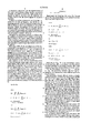
Referring to FIG. 1, a representation of the matrix-vector multiplication of two such signal sets can be seen. The matrix signal set W has matrix signals WI,J and the vector signal set V has vector signals VJ, where I is an element of the set {1,2,3, . . . ,M} and J is an element of the set {1,2,3, . . . ,K}. This can be expressed mathematically by the following formula: ##EQU1##
Such signal sets are also found in many artificial neural network models, including the Hopfield neural network model. Referring to FIG. 2, a simple artificial neural network with its associated signal sets can be seen. The first layer of neurons n1,J, or nodes, receives some form of input signals IJ, and based thereon, generates a number of voltage signals VJ, which can be represented as a voltage vector V.
Coupling the respective voltage signals VJ to the second layer of neurons n2,I are a number of scaling elements (e.g. "adaptive weights"), which introduce scaling, or "weigh," signals WI,J for scaling or "weighting" the voltage signals VJ prior to their being received by the second layer neurons n2,I. It will be understood that, with respect to the subscripted notation for representing the scaling or weighting signals WI,J, the first subscripted character "I" represents the destination neuron n2,I in the second layer, and the second subscripted character "J" represents the source neuron n1,J of the voltage signal VJ in the first layer.
The simplest form of systolic processing array used for performing the matrix-vector multiplication of signal sets, as discussed above, is one-dimensional. One type of one-dimensional systolic array is a "ring" systolic array, shown in FIG. 3.
The systolically coupled processing elements NJ are interconnected as shown, with signal flow represented by the arrows. First, the corresponding voltage signals VJ are initially coupled into their corresponding processing elements NJ. Then, following the application of each clock pulse (not shown, but common to each processing element NJ), the matrix signals WI,J are sequentially inputted to their corresponding processing element NJ, as shown. Therein, each matrix signal WI,J is multiplied by its corresponding voltage signal VJ and accumulated, i.e. stored, within the processing element NJ.
Following the next clock signal, the foregoing is repeated, with the voltage signals VJ being transferred to subsequent processing elements NJ to be multiplied by the corresponding matrix signal WI,J therein. For example, the voltage signals VJ which are transferred between the processing elements NJ are shown in parentheses. This is repeated K-1 times, i.e. for a total of K times, to produce the final matrix-vector product outputs OI. The "ring" configuration facilitates multiple iterations of the matrix-vector products, a desirable feature used in the learning phase of an artificial neural network. Further discussions of the ring systolic array can be found in "Parallel Architectures for Artificial Neural Nets," by S. Y. Kung and J. N. Hwang, IJCNN 1989, pp. II-165 through II-172.
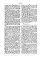
A second type of one-dimensional systolic array relies on a configuration in accordance with the "STAMS" (Systematic Transformation of Algorithms for Multidimensional Systolic arrays) technique. The STAMS technique is discussed in detail in "Algorithms for High Speed Multidimensional Arithmetic and DSP Systolic Arrays," by N. Ling and M. A. Bayoumi, Proceedings of the 1988 International Conference on Parallel Processing, Vol. I, pp. 367-374. An example of a one-dimensional STAMS systolic array is shown in FIG. 4. dimensional arrays is shorter and more processing is done in parallel. This three-dimensional configuration requires only T+K-1 clock cycles.
Even though the two-dimensional and three-dimensional STAMS systolic array configurations discussed above provide improvements with respect to processing speed, minimal if any improvement is provided with respect to the number and complexity of the local or global interconnections required for inputting the matrix W and vector V signals. Furthermore, even though the one-dimensional ring systolic array already provides reasonable processing speed, its requisite global interconnections are complex and impractical. Moreover, no improvements are provided by any of the foregoing arrays with respect to matrix signal WI,J storage requirements.
Moreover, the two- and three-dimensional STAMS systolic array configurations described above are not truly two- or three-dimensional, respectively. The two-dimensional array, as well as each two-dimensional array plane within the three-dimensional array, have their processing elements NA,B interconnected along one dimension only, e.g. left to right. Therefore, the systolic processing actually occurs in one dimension only. Thus, full multidimensional parallelism or pipelining is not achieved and maximum processing speed, i.e. minimum processing time, cannot be achieved.
It would be desirable to have a true multidimensional systolic array configuration providing true multidimensional pipeline operation to maximize processing speed. It would be further desirable to have such a multidimensional systolic processing array in which minimal global or local interconnects are required for inputting the matrix
First, just as in the ring systolic array of FIG. 3, the voltage signals VJ are initially inputted into their respective processing elements NJ. Then, the matrix signals WI,J are inputted into the processing elements NJ, with each respective processing element NJ receiving one column of the matrix of matrix signals WI,J, as shown. The weight-voltage products are summed with the corresponding weight-voltage products from the preceding processing element NJ-1 and then systolically transferred to the next processing element NJ+1, and the process continues.
The inputting of the matrix signals WI,J into each successive processing element NJ is delayed by one additional clock pulse per processing element stage to allow for the delays associated with the systolic transferring of the accumulated products. This delay can be accomplished by inputting zeros to a processing element NJ until the systolically transferred accumulated products begin to arrive. However, this delay adversely affects the processing speed. As compared to the ring systolic array of FIG. 3 which requires K clock cycles, the STAMS systolic array requires 2K-1 clock cycles to obtain the product outputs OI of this matrix-vector multiplication.
A number of problems are associated with using these one-dimensional systolic arrays. One problem involves the inputting of the voltage signals VJ. If the voltages VJ are to be loaded simultaneously in parallel, global interconnects are required to accomplish this. If they are to be loaded sequentially in serial, numerous local interconnects are required, as well as K clock cycles.
Another problem involves the inputting of the matrix signals WI,J. If the matrix signals WI,J are stored locally within each processing element NJ, the processing elements NJ must be large enough to provide sufficient storage, i.e. memory, therefor. On the other hand, if the matrix signals WI,J are not stored locally within each processing element NJ, but instead inputted as needed, the global interconnections necessary to do this become complex and impractical. Either many parallel input lines, e.g. a wide signal bus structure, or a large number of clock cycles must be provided.
A third problem involves the amount of time required to perform the matrix-vector multiplication, i.e. 2K-1 clock cycles for the STAMS systolic array. Although the ring systolic array requires only K clock cycles, the problem remains, as discussed immediately above, of providing either sufficient local matrix signal storage or complex global interconnections.
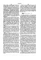
One approach to addressing these problems of interconnects, storage area and processing time involves the use of multidimensional systolic processing arrays. For example, parallelism, i.e. parallel processing, can be introduced by subdividing the matrix signals WI,J and vector signals VJ. This can be diagrammatically visualized as seen in FIGS. 5A-5B. This can be expressed mathematically by the following formula: ##EQU2##
Each row I of the matrix W is divided into P groups of Q signals WI,J. In other words, the first of the P groups of Q signals WI,J contains the matrix signals W1,1 -W1,Q. Similarly, the vector V is divided into P groups of Q voltages VJ. For example, the first of the P groups of Q voltages VJ includes the voltages V1 -VQ. This can be visualized in even simpler form as shown in FIG. 5B.
The processing of these P groups of Q signals WI,J, VJ can be accomplished by using several one-dimensional STAMS systolic arrays, such as that shown in FIG. 4, in parallel, as shown in FIG. 6A. The operation of each separate systolic array is in accordance with that described for the one-dimensional STAMS systolic array of FIG. 4 above, with the exception that only Q, rather than K, processing (i.e. clock) cycles are required for each systolic array to complete one subproduct. The subproducts of each array are then summed together to provide the final product outputs OI. Visualizing this systolic array configuration as two-dimensional is perhaps more easily done by referring to FIG. 6B.
This two-dimensional systolic array configuration is an improvement over the one-dimensional STAMS configuration, with respect to processing time. Processing time is reduced since each one-dimensional array, i.e. each pipeline of processors, within the two-dimensional array is shorter and more processing is done in parallel. This configuration requires only K+Q-1 clock cycles to obtain the product outputs OI of the matrix-vector multiplication.
Further improvement has been achieved by extending the two-dimensional STAMS systolic array of FIG. 6A to a three-dimensional systolic array. This can be done by further subdividing the matrix W and vector V signals into T groups of P groups of Q signals WI,J, VJ. This can be visualized diagrammatically by referring to FIGS. 7A-7B. This can be expressed mathematically by the following formula: ##EQU3##
As seen in FIG. 7A, each row I of the matrix W and the vector V is divided into T groups, which in turn are divided into P groups of Q signals WI,J, VJ. For example, the first of the P groups within the first of the T groups contain the matrix signals W1,1 -W1,Q and the vector signals V1 -VQ. FIG. 7B represents a more simplified depiction of this multiple subdivision of the matrix W and vector V signals.
Referring to FIG. 8A, a realization of such a three-dimensional systolic array is illustrated. Two-dimensional systolic arrays, similar to that illustrated in FIG. 6A, are disposed as if on T parallel planes. The operation of each of the T two-dimensional systolic arrays is similar to that as s described above for FIG. 6A. The subproduct outputs of each of the T two-dimensional arrays are summed together to produce the full product outputs OI. The three-dimensional nature of this array can perhaps be better visualized by referring to FIG. 8B.
This three-dimensional STAMS systolic array configuration is an improvement over the two-dimensional configuration inasmuch as fewer processing, i.e. clock, cycles are required to complete each product output OI. Processing time is reduced since each one-dimensional array, i.e. each and vector signals. It would be still further desirable to have such a multidimensional systolic processing array with minimal matrix signal storage requirements for each processing element.
SUMMARY OF THE INVENTION
A multidimensional systolic array processor in accordance with the present invention has an architecture which maximizes processing parallelism and minimizes global interconnections. Further, the present invention minimizes local matrix signal storage requirements within each processing element.
The present invention maximizes processing parallelism by interconnecting its processing elements along multiple dimensions. Therefore, systolic processing occurs along multiple dimensions. For example, a two-dimensional systolic array processor in accordance with the present invention includes a PxQ matrix having P rows and Q columns of processing elements, each of which is systolically coupled row-to-row and column-to-column for full pipeline processing within each row and each column. A three-dimensional systolic array processor has a PxQxT array with T planes of P rows and Q columns of processing elements, each of which is systolically coupled plane-to-plane-to-plane for full pipeline processing.
The present invention minimizes global interconnections of the processing elements. For the two-dimensional case, appropriate matrix and vector signal subsets are inputted to only one row and one column of the two-dimensional processing array. These matrix and vector signal subsets are specifically formed so that they need to be inputted to only one row and one column, and yet still be properly processed systolically along all dimensions within the array.
For the three-dimensional case, appropriate matrix and vector signal subsets are inputted to three perpendicular planes of the three-dimensional processing array. For higher-dimensional cases, appropriate matrix and vector signal subsets are similarly inputted to the higher-dimensional processing arrays.
The present invention minimizes local matrix signal storage requirements by inputting specifically formed matrix signal subsets to only one row and one column of the two-dimensional processing array, and to three perpendicular planes of the three-dimensional processing array. These matrix signal subsets are formed to allow the sizes of the matrix signal subsets to be reduced as they are systolically transferred to subsequent processing elements along each dimension within the array. As the matrix signal subsets decrease in size through the array, the local storage, e.g. memory, needed for temporarily storing each matrix signal subset within each processing element is successively reduced. Processing speed is not sacrificed since the matrix signal subsets are transferred to the subsequent processing element at a clock rate higher than that used for systolically transferring the vector signal subsets.
These and other objectives, features and advantages of the present invention will be understood upon consideration of the following detailed description of the invention and the accompanying drawings.
BRIEF DESCRIPTION OF THE DRAWINGS
FIG. 1 illustrates diagrammatically a conventional matrix-vector multiplication.
FIG. 2 illustrate a simple conventional two-layer artificial neural network.
FIG. 3 illustrates a conventional one-dimensional "ring" systolic array.
FIG. 4 illustrates an alternative conventional one-dimensional systolic array.
FIGS. 5A-5B illustrate diagrammatically a conventional matrix-vector multiplication, wherein the matrix and vector are subdivided into matrix and
FIGS. 6A-6B illustrate a conventional quasi two-dimensional systolic array.
FIGS. 7A-7B illustrate diagrammatically a conventional matrix-vector multiplication, wherein the matrix and vector of FIGS. 5A-5B are further subdivided into matrix and vector subsets, respectively.
FIGS. 8A-8B illustrate a conventional quasi three-dimensional systolic array.
FIG. 9 illustrates the Layer 1 and 2 neurons of FIG. 2 reconfigured as two-dimensional neural arrays in accordance with the present invention.
FIG. 10 illustrates diagrammatically the reconfiguration of the one-dimensional vector signal set of FIG. 1 into a two-dimensional vector signal set in accordance with the present invention.
FIG. 11 illustrates diagrammatically the matrix-vector multiplication of the matrix and vector column signal subsets in accordance with the present invention.
FIG. 12 illustrates diagrammatically the matrix-vector multiplication of the matrix and vector row signal subsets in accordance with the present invention.
FIG. 13 illustrates a block diagram of a two-dimensional systolic array processor in accordance with the present invention.
FIG. 14 illustrates a single processing element of the two-dimensional processor of FIG. 13.
FIG. 15 illustrates a functional block diagram of a single processing element of the two-dimensional processor of FIG. 13.
FIG. 16 illustrates the reduced local matrix signal storage requirements of the two-dimensional processor of FIG. 13.
FIG. 17 further illustrates the reduced local matrix signal storage requirements of the two-dimensional processor of FIG. 13.
FIG. 18 illustrates a block diagram of a three-dimensional systolic array processor in accordance with the present invention.
DETAILED DESCRIPTION OF THE INVENTION
Referring to FIG. 9, the Layer 1 and 2 neurons n1, n2 of an artificial neural network (as shown in FIG. 1) are reconfigured into two-dimensional neural arrays. The original input signals IJ now have double subscripted notation to reflect the two-dimensional set of input signals IY,Z. Similarly, the original voltage signals VJ now have double subscripted notation to reflect the two-dimensionality of the set of voltage signals VY,Z. Indicated in brackets for some of the Layer 1 neurons in FIG. 9 are the original Layer 1 neuron and voltage identifiers (the remaining identifiers being left out for clarity).
The Layer 2 neurons also now have double subscripted notation to reflect the new two-dimensionality of the set of Layer 2 neurons nA,B. Indicated in brackets for some of the Layer 2 neurons are the original Layer 2 neuron identifiers (the remaining identifiers being left out for clarity).
The original matrix, e.g. "weight," signals WI,J now have quadruple subscripted notation to reflect their new multidimensionality, i.e. WA,B;Y,Z. The first subscripted pair of characters "A,B" represents the destination neuron nA,B in the second layer. The second subscripted pair of characters "Y,Z" represents the source of the voltage signal VY,Z in the first layer. Indicated in brackets for some of the matrix signals WA,B;Y,Z are the original matrix signal identifiers WI,J (the remaining identifiers being left out for clarity).
It should be understood that the representations of the Layer 1 and 2 neurons, along with their subscripted notations, were selected arbitrarily. They can be reconfigured as desired, provided that the resulting subscripted notation for the matrix signals be consistent therewith.
It should be further understood that it has been assumed for the sake of simplicity that M=K for the reconfigured array of Layer 2 neurons as represented in FIG. 9. However, this is not necessary to the present invention. Ideally, the numbers of rows and columns should be equal, i.e. P=Q. This is to maximize the improvements in processing speed and to minimize the local matrix signal storage requirements in accordance with the present invention. However,
if K cannot be expressed as a square, i.e. if P≠Q, then the numbers of neurons in both Layers 1 and 2 can be approximated to the nearest square. Extra processing cycles would be required because of such an approximation, but significant improvements in processing speed and local matrix signal storage requirements would still be realized.
Referring to FIG. 10, the reconfiguration of the one-dimensional vector signal set VJ of FIG. 1 into a two-dimensional vector signal set VY,Z can be understood. The one-dimensional vector signal set VJ is initially mapped into a two-dimensional vector signal set with the original subscripted notation left intact. This two-dimensional vector signal set is then given new double subscripted notation to reflect the two-dimensionality of the reconfigured vector signal set VY,Z.
Also indicated in FIG. 10 (with dashed lines within the two-dimensional vector signal sets) are two vector signal subsets. One is referred to as the vector column signal subset VC and the other is referred to as the vector row signal subset VR. These vector signal subsets VC, VR are multiplied by the matrix signals WA,B;Y,Z as represented in FIG. 9. The matrix signals WA,B;Y,Z are separated into corresponding matrix column WC and row WR signal subsets. The vector column VC and row VR signal subsets are multiplied by the matrix column WC and row WR signal subsets, respectively, as shown in FIGS. 11 and 12. Therefore, the matrix-vector products OI are identified according to the following formulas:
O.sub.I =O.sub.C +O.sub.R ##EQU4##
Based upon the foregoing, the vector VC, VR and matrix WC, WR signal subsets can be identified according to the following formulas: ##EQU5##
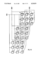
Referring to FIG. 13, a two-dimensional systolic processing array 100 in accordance with the present invention includes K processing elements 102, designated by NA,B where A is an element of the set {1,2,3, . . . ,P}, B is an element of the set {1,2,3, . . . ,Q} and K=PQ. The processing elements 102 are interconnected in a two-dimensional matrix 100 having P rows and Q columns.
The processing elements 102 are mutually coupled column-to-column via matrix row subset signal lines 104 and vector row subset signal lines 106. These signal lines 104, 106 provide the means by which the matrix WR and vector VR row signal subsets are systolically transferred column-to-column among the processing elements 102. The processing elements 102 are further mutually coupled row-to-row via matrix column subset signal lines 108 and vector column subset signal lines 110. It is by these signal lines 108, 110 that the matrix WC and vector VC signal subsets are systolically transferred row-to-row among the processing elements 102.
All processing elements 102 in the first row 112 receive a vector signal input 114 which is a vector column signal subset VC of the vector signal set V. All processing elements 102 in the first row 112 further receive a matrix signal input 116 which is a matrix column signal subset WC of the matrix signal set W.
All processing elements 102 in the first column 118 receive a vector signal input 120 which is a vector row signal subset VR of the vector signal set V. All processing elements 102 in the first column 118 further receive a matrix signal input 122 which is a matrix row signal subset WR of the matrix signal set W.
All processing elements 102 within the matrix 100 further receive two clock signals. The first clock signal, a multiply-accumulate ("MAC") clock 124, initiates and provides the timing for the multiply-accumulate operation (discussed more fully below) within each processing element 102. The second clock signal, a weight transfer ("WT") clock 126, initiates and provides the timing for the transfer of the matrix, e.g. weight, signals WI,J among the processing elements 102 (discussed more fully below).
The vector column signal subset VC is inputted in parallel to all processing elements 102 within the first row 112, one signal at a time in accordance with the MAC clock 124. As each signal of this signal subset VC is inputted, the corresponding signals in the matrix column signal subset WC (according to the formula given above) are also inputted to the processing elements 102 within the first row 112. The number of signals from the matrix column signal subset WC which are inputted with each signal of the vector column signal subset VC is P, one for each of the processing elements 102 in each column (discussed more fully below).
Similarly, the vector row signal subset VR is inputted in parallel to all processing elements 102 in the first column 118, one signal at a time in accordance with the MAC clock 124. Inputted in parallel therewith are the corresponding signals from the matrix row signal subset WR (according to the formula given above). The number of these corresponding signals within the matrix row signal subset WR is Q, one for each processing element 102 within each row (discussed more fully below).
As discussed further below, the matrix WC and vector VC column signal subsets and matrix WR and vector VR row signal subsets are multiplied simultaneously and then added in each processing element 102. After completing the matrix-vector subproducts and accumulation thereof for the first column and row signals of the column WC, VC and row WR, VR signal subsets, this process is repeated for the second column and row signals. However, as discussed further below, the matrix column WC and row WR signal subsets each contain fewer signals following each multiplication and accumulation.
The number of signals to be transferred within each matrix column WC or row WR signal subset is greater than the corresponding signal in the vector column VR or row VR signal subset, respectively. Therefore, the row-to-row or column-to-column transferring of the matrix column WC and row WR signal subsets should be done at a higher rate than the corresponding transfer of the vector column VC and row VR signal subsets, respectively. Thus, the WT clock 126 operates at a higher frequency than the MAC clock 124.
The rate of the WT clock 126 is the greater of either P- or Q- times that of the MAC clock 124. It will be understood that this provides for transferring all corresponding matrix signals WC, WR (P signals from the matrix column signal subset WC, and Q signals from the matrix row signal subset WR) "simultaneously" with their corresponding vector signal subsets VC, VR. Processing speed is not sacrificed for this, since the multiply-accumulate operation performed on each vector signal subset VC, VR requires more time than the mere transfer of one matrix signal WI,J to the next processing element 102.
Referring to FIG. 14, a single processing element NA,B representative of all processing elements 102 within the matrix 100 is illustrated. As discussed above, input signals 104a, 106a, 108a, 110a include the matrix WR and vector VC row signal subsets, and matrix WC and vector VC column signal subsets which are systolically transferred from prior processing elements 102 in the preceding column and row, respectively. Further input signals, as discussed above, include the MAC clock 124 and WT clock 126.
Output signals 104b, 106b, 108b, 110b include the matrix WR and vector VR row signal subsets, and the matrix WC and vector VC column signal subsets which are systolically transferred to subsequent processing elements 102 in the next column and row, respectively. As discussed more fully below, the output matrix WR, WC signal subsets 104b, 108b contain fewer members, i.e. signals, than their corresponding input matrix WR, WC signal subsets 104a, 108a. Another output signal 12B is the matrix-vector subproduct signal OI.
The two-dimensional operation of the systolic processing array 100 in accordance with the present invention, as shown in FIG. 9, is substantially faster. It can be shown that the total processing, e.g. computation, time is P(P+1)/2-(P/2)+P cycles (i.e. of MAC clock 124). This is substantially faster than the quasi two-dimensional array of FIG. 6A discussed above. Mathematically, the improvement in processing speed can be expressed by the following formula: ##EQU6##
For example, if P=Q=10 (and therefore K=100), the quasi two-dimensional array of FIG. 6A requires Q+K-1=10+100-1=109 cycles. The array 100 of the present invention, however, only requires 10(10+1)/2-(10/2)+10=60 cycles. As the array 100 size increases, i.e. as P and Q become greater, the improvement in processing speed of the present invention is enhanced further. It can be shown that this improvement becomes enhanced by as much as 50% over that of the quasi two-dimensional array of FIG. 6A.
Referring to FIG. 15, the operation, e.g. multiply-accumulate (MAC) function, of each processing element 102 can be understood. The matrix WR, WC signal subsets are inputted and stored in matrix storage elements 204, 208 (e.g. memory circuits or registers). The corresponding vector VR, VC signal subsets are inputted and selectively stored in vector signal storage elements 206, 210 (e.g. memory circuits or registers). The corresponding matrix WC and vector VC column signals are then multiplied, as are the corresponding matrix WR and vector VR row signals in multipliers 212, 214. It should be understood that the vector VR, VC signal subsets need not necessarily be stored, but instead can be inputted directly into their respective multipliers 212, 214.
The resulting matrix-vector subproducts are then summed together in an adder 216. It will be recognized that this multiplication and summation can be done with digital multipliers and adders, or alternatively, a microprocessor can be programmed to perform this. The remaining matrix WR, WC and vector VR, VC signal subsets are then systolically transferred to subsequent processing elements 102.
Referring to FIG. 16, the systolic transferring and local storage of successively smaller groups of signals from the matrix column signal subset WC can be understood. As discussed above, the matrix column signal subset WC initially has P members, i.e. signals, for each corresponding signal from the vector column signal subset VC. These corresponding matrix WC and vector VC signal subsets are then transferred to the second processing element N2,1 in the first column 118 via the matrix 108 and vector 110 column subset signal lines.
However, as discussed above for FIG. 11, the first of the signals within the matrix column signal subset WC corresponding to the inputted signal from the vector column signal subset VC has already been processed and is no longer needed. Therefore it need not be transferred, i.e. only P-1 signals of the matrix column signal subset WC need to be transferred to the second processing element N2,1. Therefore, whereas the storage registers, e.g. memory, within the first processing element N1,1 must be large enough to store P matrix signals, the corresponding registers within the second processing element N2,1 need only be large enough to store P-1 matrix signals.
Similarly, the third processing element N3,1 need only store P-2 matrix signals, and so on. This continues until the last processing element NP,1 which need only contain enough storage area to store one matrix signal. Thus, it can be seen that local storage requirements for the matrix column signal subsets WC for all processing elements 102 within the first column 118 total P(P+1)/2 storage registers. Since each of the Q columns of processing elements 102 are identical, total storage requirements for the full array 100 for the matrix column signal subsets WC are QP(P+1)/2 storage registers.
Referring to FIG. 17, the reduced local storage requirements for the matrix row signal subsets WR can similarly be understood. As discussed above, corresponding signals from the vector VR and matrix WR row signal subsets are inputted into each processing element 102 in the first row 112 of the array 100. As the vector row signal subset VR is systolically processed and transferred column-to-column through the array 100, its corresponding matrix row signal subset WR is transferred therewith.
However, as discussed above, the number of corresponding signals within the transferred matrix row signal subset WR is reduced by one signal with each systolic processing cycle and transfer. For example, the first processing element N1,1 in the first row 112 of processing elements 102 receives a signal from the vector row signal subset VR, and a corresponding group of signals from the corresponding matrix row signal subset WR, which has Q members, i.e. signals. After processing by the first processing element N1,1, the first matrix signal within the matrix row signal subset WR is no longer needed, and therefore need not be transferred to the second processing element N1,2. Thus, only Q-1 signals of the matrix row signal subset WR are transferred and stored within the second processing element N1,2.
This continues to be true as the vector VR and matrix WR row signal subsets are systolically processed and transferred column-to-column through the array 100. Thus, the last processing element N1,Q need provide local storage registers for only one signal from the matrix row signal subset WR.
Based upon the foregoing, it can be shown that the total local storage requirements for all processing elements 102 within each row are Q(Q+1)/2 storage registers. Including all P rows of processing elements 102, the total local storage requirements for storing the matrix row signal subsets WR are PQ(Q+1)/2 storage registers.
Therefore, it can be shown that for the case of P=Q and K=PQ, the total local storage requirements for both the matrix column WC and row WR signal subsets are P2 (P+1) storage registers. This represents a significant improvement over the local storage requirements of the quasi two-dimensional array of FIG. 6A. For example, for the case of P=Q and K=PQ, local matrix signal storage requirements are reduced approximately by a factor of P, or more precisely, according to the following formula: ##EQU7##
It should be understood that the foregoing principles of a two-dimensional systolic array in accordance with the present invention can also be extended to a three-dimensional systolic array. In such a three-dimensional systolic array, all adjacent processing elements along all three dimensions are mutually coupled for systolically processing and transferring the matrix and vector signal subsets. Whereas the quasi three-dimensional systolic array of FIG. 8A requires T+K-1 processing cycles to produce the product outputs OI, a fully three-dimensional systolic array in accordance with the present invention requires only approximately P(P+1)(2P+1)/12 processing cycles (for P=Q=T).
Referring to FIG. 18, a block diagram of a three-dimensional systolic processing array in accordance with the present invention for P=Q=T=3 is illustrated. Pipelining is done in all three dimensions simultaneously as shown. The matrix WP1, WP2, WP3 and vector VP1, VP2, VP3 signal subsets are inputted to three perpendicular planes of processing elements. As in the two-dimensional case discussed above, the corresponding matrix and vector signals are inputted into their respective processing elements sequentially, multiplied and accumulated therein. The remaining corresponding matrix and vector signals are then systolically transferred to subsequent processing elements plane-by-plane-by-plane throughout the three-dimensional processing array.
It will be recognized that the "cube" to which the corresponding matrix and vector signals are transferred becomes smaller by one processing element on all sides. For example, starting at a corner processing element N1,1,1, the matrix WP1, WP2, WP3 and vector VP1, VP2, VP3 signal subsets are initially inputted to three perpendicular planes of processing elements. The matrix and vector signals are then systolically transferred to subsequent processing elements plane-by-plane-by-plane throughout the three-dimensional processing array, with a new "corner" processing element N2,2,2 located one processing element in from the initial corner processing element N1,1,1.
Hence, it can be seen from the foregoing that a multidimensional systolic array processor in accordance with the present invention provides improved processing speed due to the full multidimensionality of its processing element interconnections, improved global interconnectivity (e.g. by requiring external connections to only one row and one column of the two-dimensional array), and reduced local storage requirements by avoiding the unnecessary transferring and local storage of unneeded matrix signals.
It should be understood that various alternatives to the embodiments of the present invention described herein can be employed in practicing the present invention. It is intended that the following claims define the scope of the present invention, and that structures and methods within the scope of these claims and their equivalents be covered thereby.

Claims (45)

What is claimed is:
1. A multidimensional systolic array processor comprising:
a signal processing array systolically coupled in a PxQ matrix having P rows and Q columns of processing means NA,B, where Aε{1,2,3, . . . ,P} and Bε{1,2,3, . . . ,Q}, to systolically process a matrix signal set W having a plurality of matrix signals WI,J and a vector signal set V having a plurality of vector signals VJ, where Iε{1,2,3, . . . M} and Jε{1,2,3, . . . ,K}, said matrix signal set W representing a matrix parameter set selectively represented as an MxK matrix having M rows and K columns f parameters, and said vector signal set V representing a vector element vector having K parameters, wherein each processing means N1,B in a first one of said rows of processing means NA,B is coupled to receive a vector column signal subset VC of said vector signal set V, wherein said vector column signal subset VC includes a first subplurality of said plurality of vector signals VJ and where
V.sub.C =V.sub.Y,Z =V.sub.J ##EQU8##
2. An array processor as recited in claim 1, wherein each processing means NA,1 in a first one of said columns of processing means NA,B is coupled to receive a vector row signal subset VR of said vector signal set V, wherein said vector row signal subset VR includes a second subplurality of said plurality of vector signals VJ and where
V.sub.R =V.sub.Y,Z =V.sub.J ##EQU9##
3. An array processor as recited in claim 1, wherein said systolic coupling of said processing means NA,B comprises individually coupling each processing means NA,B in each row with a corresponding processing means NA-1,B in a preceding row via a vector column subset signal line LVC(A-1) and a matrix column subset signal line LWC(A-1), and individually coupling each processing means NA,B in each row with a corresponding processing means NA+1,B in a subsequent row via a vector column subset signal line LVC(A+1) and a matrix column subset signal line LWC(A+1).
4. An array processor as recited in claim 2, wherein said systolic coupling of said processing means NA,B comprises individually coupling each processing means NA,B in each column with a corresponding processing means NA,B-1 in a preceding column via a vector row subset signal line LVR(B-1) and a matrix row subset signal line LWR(B-1), and individually coupling each processing means NA,B in each column with a corresponding processing means NA,B+1 in a subsequent column via a vector row subset signal line LVR(B+1) and a matrix row subset signal line LWR(B+1).
5. An array processor as recited in claim 1, wherein each one of said processing means N1,B in said first row of processing means NA,B is coupled to receive said vector column signal subset VC substantially simultaneously.
6. An array processor as recited in claim 2, wherein each one of said processing means NA,1 in said first column of processing means NA,B is coupled to receive said vector row signal subset VR substantially simultaneously.
7. An array processor as recited in claim 1, wherein each one of said processing means NA,B comprises a multiplier-accumulator.
8. An array processor as recited in claim 7, wherein said multiplier-accumulator comprises a digital adder and a digital register.
9. An array processor as recited in claim 1, wherein each one of said processing means NA,B comprises a plurality of digital registers.
10. A multidimensional systolic array processor comprising:
a signal processing array systolically coupled in a PxQ matrix having P rows and Q columns of processing means NA,B, where Aε{1,2,3, . . . ,P} and Bε{1,2,3, . . . ,Q}, to systolically process a matrix signal set W having a plurality of matrix signals WI,J and a vector signal set V having a plurality of vector signals VJ, where Iε{1,2,3, . . . ,M} and Jε{1,2,3, . . . K}, said matrix signal set W representing a matrix parameter set selectively represented as an MxK matrix having M rows and K columns of parameters, and said vector signal set V representing a vector parameter set selectively represented as a K-element vector having K parameters, wherein each processing means N1,B in a first one of said rows of processing means NA,B is coupled to receive a matrix column signal subset WC of said matrix signal set W, wherein said matrix column signal subset WC includes a first subplurality of said plurality of matrix signals WI,J and where
W.sub.C =W.sub.A,B;Y,Z ##EQU10##  and further wherein said matrix column signal subset W.sub.C is systolically coupled row-to-row within said matrix of processing means N.sub.A,B, said coupled matrix column signal subset W.sub.C having a second subplurality of said matrix signals W.sub.I,J as said matrix column signal subset W.sub.C is coupled from one of said rows of processing means N.sub.A,B to a subsequent row of processing means N.sub.A+1,B, and still further wherein said second subplurality of matrix signals W.sub.I,J is smaller than said first subplurality of matrix signals W.sub.I,J.
11. An array processor as recited in claim 10, wherein each processing means NA,B is coupled to receive a matrix row signal subset WR of said matrix signal set W, wherein said matrix row signal subset WR includes a third subplurality of said plurality of matrix signals WI,J and where
W.sub.R =W.sub.A,B;Y,Z ##EQU11## and further wherein said matrix row signal subset W.sub.R is systolically coupled column-to-column within said matrix of processing means N.sub.A,B, said coupled matrix row signal subset W.sub.R having a fourth subplurality of said matrix signals W.sub.I,J as said matrix row signal subset W.sub.R is coupled from one of said columns of processing means N.sub.A,B to a subsequent column of processing means N.sub.A,B+1, and still further wherein said fourth subplurality of matrix signals W.sub.I,J is smaller than said third subplurality of matrix signals W.sub.I,J.
12. An array processor as recited in claim 10, wherein said systolic coupling of said processing means NA,B comprises individually coupling each processing means NA,B in each row with a corresponding processing means NA-1,B in a preceding row via a vector column subset signal line LVC(A-1) and a matrix column subset signal line LWC(A-1), and individually coupling each processing means NA,B in each row with a corresponding processing means NA+1,B in a subsequent row via a vector column subset signal line VC(A+1) and a matrix column subset signal line LWC(A+1).
13. An array processor as recited in claim 11, wherein said systolic coupling of said processing means NA,B comprises individually coupling each processing means NA,B in each column with a corresponding processing means NA,B-1 in a preceding column via a vector row subset signal line LVR(B-1) and a matrix row subset signal line LWR(B-1), and individually coupling each processing means NA,B in each column with a corresponding processing means NA,B+1 in a subsequent column via a vector row subset signal line LVR(B+1) and a matrix row subset signal line LWR(B+1).
14. An array processor as recited in claim 10, wherein each one of said processing means N1,B in said first row of processing means NA,B is coupled to receive said matrix column signal subset WC substantially simultaneously.
15. An array processor as recited in claim 11, wherein each one of said processing means NA,1 in said first column of processing means NA,B is coupled to receive said matrix row signal subset WR substantially simultaneously.
16. An array processor as recited in claim 10, wherein each one of said processing means NA,B comprises a multiplier-accumulator.
17. An array processor as recited in claim 16, wherein said multiplier-accumulator comprises a digital adder and a digital register.
18. An array processor as recited in claim 10, wherein each one of said processing means NA,B comprises a plurality of digital registers.
19. A multidimensional systolic array processor comprising:
a signal processing array systolically coupled in a PxQ matrix having P rows and Q columns of processing means NA,B, where Aε{1,2,3, . . . P} and Bε{1,2,3, . . . Q}, to systolically process a matrix signal set W having a plurality of matrix signals WI,J and a vector signal set V having a plurality of vector signals VJ, where Iε{1,2,3, . . . M} and Jε{1,2,3, . . . K}, said matrix signal set W representing a matrix parameter set selectively represented as an MxK matrix having M rows and K columns of parameters, and said vector signal set V represented as a K-element vector having K parameters, wherein each processing means N1,B in a first one of said rows of processing means NA,B is coupled to receive a vector column signal subset VC of said vector signal set V, wherein said vector column signal subset VC includes a first subplurality of said plurality of vector signals VJ and where
V.sub.C =V.sub.Y,Z =V.sub.J ##EQU12##  and further wherein each processing means N.sub.1,B in a first one of said rows of processing means N.sub.A,B is coupled to receive a matrix column signal subset W.sub.C of said matrix signal set W, wherein said matrix column signal subset W.sub.C includes a second subplurality of said plurality of matrix signals W.sub.I,J and where
W.sub.C =W.sub.A,B;Y,Z ##EQU13##  and still further wherein said matrix column signal subset W.sub.C is systolically coupled row-to-row within said matrix of processing means N.sub.A,B, said coupled matrix column signal subset W.sub.C having a third subplurality of said matrix signals W.sub.I,J as said matrix column signal subset W.sub.C is coupled from one of said rows of processing means N.sub.A,B to a subsequent row of processing means N.sub.A+1,B, and still further wherein said third subplurality of matrix signals W.sub.I,J is smaller than said second subplurality of matrix signals W.sub.I,J.
20. An array processor as recited in claim 19, wherein each processing means NA,1 in a first one of said columns of processing means NA,B is coupled to receive a vector row signal subset VR of said vector signal set V, wherein said vector row signal subset VR includes a fourth subplurality of said plurality of vector signals VJ and where
V.sub.R =V.sub.Y,Z =V.sub.J ##EQU14##
21. An array processor as recited in claim 20, wherein each processing means NA,1 in a first one of said columns of processing means NA,B is coupled to receive a matrix row signal subset WR of said matrix signal set W, wherein said matrix row signal subset WR includes a fifth subplurality of said plurality of matrix signals WI,J and where
W.sub.R =W.sub.A,B;Y,Z ##EQU15## and further wherein said matrix row signal subset W.sub.R is systolically coupled column-to-column within said matrix of processing means N.sub.A,B, said coupled matrix row signal subset W.sub.R having a sixth subplurality of said matrix signal W.sub.I,J as said matrix row signal subset W.sub.R is coupled from one of said columns of processing means N.sub.A,B to a subsequent column of processing means N.sub.A,B+1, and still further wherein said sixth subplurality of matrix signals W.sub.I,J is smaller than said fifth subplurality of matrix signals W.sub.I,J.
22. An array processor as recited in claim 19, wherein said systolic coupling of said processing means NA,B comprises individually coupling each processing means NA,B in each row with a corresponding processing means NA-1,B in a preceding row via a vector column subset signal line LVC(A-1) and a matrix column subset signal line LWC(A-1), and individually coupling each processing means NA,B in each row with a corresponding processing means NA+1,B in a subsequent row via a vector column subset signal line LVC(A+1) and a matrix column subset signal line LWC(A+1).
23. An array processor as recited in claim 20, wherein said systolic coupling of said processing means NA,B comprises individually coupling each processing means NA,B in each column with a corresponding processing means NA,B-1 in a preceding column via a vector row subset signal line LVR(B-1) and a matrix row subset signal line LWR(B-1), and individually coupling each processing means NA,B in each column with a corresponding processing means NA,B+1 in a subsequent column via a vector row subset signal line LVR(B+1) and a matrix row subset signal line LWR(B+1).
24. An array processor as recited in claim 19, wherein each one of said processing means N1,B in said first row of processing means NA,B is coupled to receive said vector column signal subset VC substantially simultaneously.
25. An array processor as recited in claim 20, wherein each one of said processing means NA,1 in said first column of processing means NA,B is coupled to receive said vector row signal subset VR substantially simultaneously.
26. An array processor as recited in claim 19, wherein each one of said processing means N1,B in said first row of processing means NA,B is coupled to receive said matrix column signal subset WC substantially simultaneously.
27. An array processor as recited in claim 20, wherein each one of said processing means NA,1 in said first column of processing means NA,B is coupled to receive said matrix row signal subset WR substantially simultaneously.
28. An array processor as recited in claim 19, wherein each one of said processing means NA,B comprises a multiplier-accumulator.
29. An array processor as recited in claim 28, wherein said multiplier-accumulator comprises a digital adder and a digital register.
30. An array processor as recited in claim 19, wherein each one of said processing means NA,B comprises a plurality of digital registers.
31. A method of systolically processing a plurality of signal sets, comprising the steps of:
(a) providing a signal processing array systolically coupled in a PxQ matrix having P rows and Q columns of processing means NA,B, where Aε{1,2,3, . . . P} and Bε{1,2,3, . . . Q};
(b) coupling into said processing array a matrix signal set W having a plurality of matrix signal WI,J representing a matrix parameter set selectively represented as an MxK matrix having M rows and K columns of parameters, where Iε{1,2,3, . . . M} and Jε{1,2,3, . . . K};
(c) coupling into said processing array a vector signal set V having a plurality of vector signals VJ representing a vector parameter set selectively represented as a K-element vector having K parameters, wherein a vector column signal subset VC of said vector signal set V is coupled into each processing means N1,B in a first one of said rows of processing means NA,B, wherein said vector column signal subset VC includes a first subplurality of said plurality of vector signals VJ and where
V.sub.C =V.sub.Y,Z =V.sub.J ##EQU16## (d) systolically processing said matrix W and vector V signal sets.
32. A processing method as recited in claim 31, wherein said step (c) of coupling said vector signal set V into said processing array further comprises coupling a vector row signal subset VR of said vector signal set V into each processing means NA,1 in a first one of said columns of processing means NA,B, wherein said vector row signal subset VR includes a second subplurality of said plurality of vector signals VJ and where
V.sub.R =V.sub.Y,Z =V.sub.J ##EQU17##
33. A processing method as recited in claim 31, wherein said step (c) of coupling said vector signal set V into said processing array further comprises coupling said vector column signal subset VC into each one of said processing means N1,B in said first row of processing means NA,B substantially simultaneously.
34. A processing method as recited in claim 32, wherein said step (c) of coupling said vector signal set V into said processing array further comprises coupling said vector row signal subset VR into each one of said processing means NA,1 in said first column of processing means NA,B substantially simultaneously.
35. A method of systolically processing a plurality of signal sets, comprising the steps of:
(a) providing a signal processing array systolically coupled in a PxQ matrix having P rows and Q columns of processing means NA,B, where Aε{1,2,3, . . . P} and Bε{1,2,3, . . . Q};
(b) coupling into said processing array a matrix signal set W having a plurality of matrix signals WI,J representing a matrix parameter set selectively represented as an MxK matrix having M rows of K columns of parameters, where Iε{1,2,3, . . . M} and J{1,2,3, . . . K}, wherein a matrix column signal subset WC of said matrix signal set W is coupled into each processing means N1,B in a first one of said rows of processing means NA,B, wherein said matrix column signal subset WC includes a first subplurality of said plurality of matrix signals WI,J and where
W.sub.C =W.sub.A,B;Y,Z ##EQU18##  and further wherein said matrix column signal subset W.sub.C is systolically coupled row-to-row within said matrix of processing means N.sub.A,B, said coupled matrix column signal subset W.sub.C having a second subplurality of said matrix signals W.sub.I,J as said matrix column signal subset W.sub.C is coupled from one of said rows of processing means N.sub.A,B to a subsequent row of processing means N.sub.A+1,B, and still further wherein said second subplurality of matrix signals W.sub.I,J is smaller than said first subplurality of matrix signals W.sub.I,J ;
(c) coupling into said processing array a vector signal set V having a plurality of vector signals VJ representing a vector parameter set selectively represented as a K-element vector having K parameters; and
(d) systolically processing said matrix W and vector V signal sets.
36. A processing method as recited in claim 35, wherein said step of (b) coupling said matrix signal set W into said processing array further comprises coupling a matrix row signal subset WR of said matrix signal set W into each processing means NA,1 in a first one of said columns of processing means NA,B, wherein said matrix row signal subset WR includes a third subplurality of said plurality of matrix signals WI,J and where
W.sub.R =W.sub.A,B;Y,Z ##EQU19## and further wherein said matrix row signal subset W.sub.R is systolically coupled column-to-column within said matrix of processing means N.sub.A,B, said coupled matrix row signal subset W.sub.R having a fourth subplurality of said matrix signals W.sub.I,J as said matrix row signal subset W.sub.R is coupled from one of said columns of processing means N.sub.A,B to a subsequent column of processing means N.sub.A,B+1, and still further wherein said fourth subplurality of matrix signals W.sub.I,J is smaller than said third subplurality of matrix signals W.sub.I,J.
37. A processing method as recited in claim 35, wherein said step of (b) coupling said matrix signal set W into said processing array further comprises coupling said matrix column signal subset WC into each one of said processing means N1,B in said first row of processing means NA,B substantially simultaneously.
38. A processing method as recited in claim 36, wherein said step of (b) coupling said matrix signal set W into said processing array further comprises coupling said matrix row signal subset WR into each one of said processing means NA,1 in said first column of processing means NA,B substantially simultaneously.
39. A method of systolically processing a plurality of signal sets, comprising the steps of:
(a) providing a signal processing array systolically coupled in a PxQ matrix having P rows and Q columns of processing means NA,B, where Aε{1,2,3, . . . P} and Bε{1,2,3, . . . Q};
(b) coupling into said processing array a matrix signal set W having a plurality of matrix signal WI,J representing a matrix parameter set selectively represented as an MxK matrix having M rows and K columns of parameters, where Iε{1,2,3, . . . M} and Jε{1,2,3, . . . K}, wherein a matrix column signal subset WC of said matrix signal set W is coupled into each processing means N1,B in a first one of said rows of processing means NA,B, wherein said matrix column signal subset WC includes a first subplurality of said plurality of matrix signals WI,J and where
W.sub.C =W.sub.A,B;Y,Z ##EQU20##  and further wherein said matrix column signal subset W.sub.C is systolically coupled row-to-row within said matrix of processing means N.sub.A,B, said coupled matrix column signal subset W.sub.C having a second subplurality of said matrix signals W.sub.I,J as said matrix column signal subset W.sub.C is coupled from one of said rows of processing means N.sub.A,B to a subsequent row of processing means N.sub.A+1,B, and still further wherein said third subplurality of matrix signals W.sub.I,J is smaller than said second subplurality of matrix signals W.sub.I,J ;
(c) coupling into said processing array a vector signal set V having a plurality of vector signals VJ representing a vector parameter set selectively represented as a K-element vector having K parameters, wherein a vector column signal subset VC of said vector signal set V is coupled into each processing means N1,B in a first one of said rows of processing means NA,B, wherein said vector column signal subset VC includes a first subplurality of said plurality of vector signals VJ and where
V.sub.C =V.sub.Y,Z =V.sub.J ##EQU21## (d) systolically processing said matrix W and vector V signal sets.
40. A processing method as recited in claim 39, wherein said set of (b) coupling said matrix signal set W into said processing array further comprises coupling a matrix row signal subset WR of said matrix signal set W into each processing means NA,1 in a first one of said columns of processing means NA,B, wherein said matrix row signal subset WR includes a fourth subplurality of said plurality of matrix signals WI,J and where
W.sub.R =W.sub.A,B;Y,Z ##EQU22## and further wherein said matrix row signal subset W.sub.R is systolically coupled column-to-column within said matrix of processing means N.sub.A,B, said coupled matrix row signal subset W.sub.R having a fifth subplurality of said matrix signals W.sub.I,J as said matrix row signal subset W.sub.R is coupled from one of said columns of processing means N.sub.A,B to a subsequent column of processing means N.sub.A,B+1, and still further wherein said fifth subplurality of matrix signals W.sub.I,J is smaller than said third subplurality of matrix signals W.sub.I,J.
41. A processing method as recited in claim 39, wherein said step (b) coupling said matrix signal set W into said processing array further comprises coupling said matrix column signal subset WC into each one of said processing means N1,B in said first row of processing means NA,B substantially simultaneously.
42. A processing method as recited in claim 40, wherein said step of (b) coupling said matrix signal set W into said processing array further comprises coupling said matrix row signal subset WR into each one of said processing means NA,1 in said first column of processing means NA,B substantially simultaneously.
43. A processing method as recited in claim 39, wherein said step (c) of coupling said vector signal set V into said processing array further comprises coupling a vector row signal subset VR of said vector signal set V into each processing means NA,1 in a first one of said columns of processing means NA,B, wherein said vector row signal subset VR includes a sixth subplurality of said plurality of vector signals VJ and where
V.sub.R =V.sub.Y,Z =V.sub.J ##EQU23##
44. A processing method as recited in claim 39, wherein said step (c) of coupling said vector signal set V into said processing array further comprises coupling said vector column signal subset VC into each one of said processing means N1,B in said first row of processing means NA,B substantially simultaneously.
45. A processing method as recited in claim 43, wherein said step (c) of coupling means vector signal set V into said processing array further comprises coupling said vector row signal subset VR into each one of said processing means NA,1 in said first column of processing means NA,B substantially simultaneously.
US07/592,954 1990-10-04 1990-10-04 Systolic array for multidimensional matrix computations Expired - Lifetime US5274832A (en)

Priority Applications (3)

Application Number Priority Date Filing Date Title
US07/592,954 US5274832A (en) 1990-10-04 1990-10-04 Systolic array for multidimensional matrix computations
EP19910116286 EP0479102A3 (en) 1990-10-04 1991-09-25 Multidimensional systolic array processing apparatus and method
JP3255405A JPH06131308A (en) 1990-10-04 1991-10-02 Device and method for processing multidimensional systolic array

Applications Claiming Priority (1)

Application Number Priority Date Filing Date Title
US07/592,954 US5274832A (en) 1990-10-04 1990-10-04 Systolic array for multidimensional matrix computations

Publications (1)

Publication Number Publication Date
US5274832A true US5274832A (en) 1993-12-28

Family

ID=24372737

Family Applications (1)

Application Number Title Priority Date Filing Date
US07/592,954 Expired - Lifetime US5274832A (en) 1990-10-04 1990-10-04 Systolic array for multidimensional matrix computations

Country Status (3)

Country Link
US (1) US5274832A (en)
EP (1) EP0479102A3 (en)
JP (1) JPH06131308A (en)

Cited By (28)

* Cited by examiner, † Cited by third party
Publication number Priority date Publication date Assignee Title
US5430887A (en) * 1992-10-19 1995-07-04 General Electric Company Cube-like processor array architecture
US5434932A (en) * 1994-07-28 1995-07-18 West Publishing Company Line alignment apparatus and process
US5481748A (en) * 1991-12-13 1996-01-02 International Business Machines Corporation Method and apparatus for reducing the processing time required to solve numerical problems
US5490278A (en) * 1991-07-12 1996-02-06 Matsushita Electric Industrial Co., Ltd. Data processing method and apparatus employing parallel processing for solving systems of linear equations
US5524090A (en) * 1992-06-25 1996-06-04 Canon Kabushiki Kaisha Apparatus for multiplying long integers
US5630154A (en) * 1994-10-11 1997-05-13 Hughes Aircraft Company Programmable systolic array system arranged in a found arrangement for passing data through programmable number of cells in a time interleaved manner
US5675823A (en) * 1995-08-07 1997-10-07 General Electric Company Grain structured processing architecture device and a method for processing three dimensional volume element data
US5680515A (en) * 1993-04-19 1997-10-21 California Institute Of Technology High precision computing with charge domain devices and a pseudo-spectral method therefor
US5715471A (en) * 1994-03-14 1998-02-03 Fujitsu Limited Parallel computer
US5748942A (en) * 1995-06-07 1998-05-05 Xilinx, Inc. Efficient three-dimensional layout method for logic cell arrays
US5799134A (en) * 1995-03-13 1998-08-25 Industrial Technology Research Institute One dimensional systolic array architecture for neural network
US6023742A (en) * 1996-07-18 2000-02-08 University Of Washington Reconfigurable computing architecture for providing pipelined data paths
US6405185B1 (en) * 1992-04-06 2002-06-11 International Business Machines Corporation Massively parallel array processor
US20040088527A1 (en) * 2002-10-31 2004-05-06 Huppenthal Jon M. Multi-adaptive processing systems and techniques for enhancing parallelism and performance of computational functions
WO2006116044A2 (en) * 2005-04-22 2006-11-02 Altrix Logic, Inc. Array of data processing elements with variable precision interconnect
US20070192241A1 (en) * 2005-12-02 2007-08-16 Metlapalli Kumar C Methods and systems for computing platform
US20080028015A1 (en) * 2006-07-21 2008-01-31 Nec Electronics Corporation Systolic array
US8788556B2 (en) 2011-05-12 2014-07-22 Microsoft Corporation Matrix computation framework
US8924455B1 (en) * 2011-02-25 2014-12-30 Xilinx, Inc. Multiplication of matrices using systolic arrays
US9910826B2 (en) 2015-03-27 2018-03-06 International Business Machines Corporation SIMD implementation of stencil codes
US10055672B2 (en) 2015-03-11 2018-08-21 Microsoft Technology Licensing, Llc Methods and systems for low-energy image classification
US10241972B2 (en) * 2017-03-16 2019-03-26 International Business Machines Corporation Matrix multiplication on a systolic array
US10268886B2 (en) 2015-03-11 2019-04-23 Microsoft Technology Licensing, Llc Context-awareness through biased on-device image classifiers
US10517540B1 (en) 2018-08-06 2019-12-31 Hi Llc Systems and methods to reduce data and complexity in neural signal processing chain
US20200192701A1 (en) * 2017-09-21 2020-06-18 Huawei Technologies Co., Ltd. Multi-thread systolic array
CN112632464A (en) * 2020-12-28 2021-04-09 上海壁仞智能科技有限公司 Processing device for processing data
US11341086B2 (en) * 2019-11-22 2022-05-24 Rambus Inc. Compute accelerator with 3D data flows
US11907826B2 (en) 2017-03-23 2024-02-20 Samsung Electronics Co., Ltd Electronic apparatus for operating machine learning and method for operating machine learning

Families Citing this family (22)

* Cited by examiner, † Cited by third party
Publication number Priority date Publication date Assignee Title
US7752419B1 (en) 2001-03-22 2010-07-06 Qst Holdings, Llc Method and system for managing hardware resources to implement system functions using an adaptive computing architecture
US7962716B2 (en) 2001-03-22 2011-06-14 Qst Holdings, Inc. Adaptive integrated circuitry with heterogeneous and reconfigurable matrices of diverse and adaptive computational units having fixed, application specific computational elements
US7653710B2 (en) 2002-06-25 2010-01-26 Qst Holdings, Llc. Hardware task manager
US7249242B2 (en) 2002-10-28 2007-07-24 Nvidia Corporation Input pipeline registers for a node in an adaptive computing engine
US6836839B2 (en) 2001-03-22 2004-12-28 Quicksilver Technology, Inc. Adaptive integrated circuitry with heterogeneous and reconfigurable matrices of diverse and adaptive computational units having fixed, application specific computational elements
US6577678B2 (en) 2001-05-08 2003-06-10 Quicksilver Technology Method and system for reconfigurable channel coding
US7046635B2 (en) 2001-11-28 2006-05-16 Quicksilver Technology, Inc. System for authorizing functionality in adaptable hardware devices
US8412915B2 (en) 2001-11-30 2013-04-02 Altera Corporation Apparatus, system and method for configuration of adaptive integrated circuitry having heterogeneous computational elements
US6986021B2 (en) 2001-11-30 2006-01-10 Quick Silver Technology, Inc. Apparatus, method, system and executable module for configuration and operation of adaptive integrated circuitry having fixed, application specific computational elements
US7215701B2 (en) 2001-12-12 2007-05-08 Sharad Sambhwani Low I/O bandwidth method and system for implementing detection and identification of scrambling codes
US6947916B2 (en) 2001-12-21 2005-09-20 Quicksilver Technology, Inc. IC for universal computing with near zero programming complexity
US7403981B2 (en) 2002-01-04 2008-07-22 Quicksilver Technology, Inc. Apparatus and method for adaptive multimedia reception and transmission in communication environments
US7328414B1 (en) 2003-05-13 2008-02-05 Qst Holdings, Llc Method and system for creating and programming an adaptive computing engine
US7660984B1 (en) 2003-05-13 2010-02-09 Quicksilver Technology Method and system for achieving individualized protected space in an operating system
US8108656B2 (en) 2002-08-29 2012-01-31 Qst Holdings, Llc Task definition for specifying resource requirements
US7937591B1 (en) 2002-10-25 2011-05-03 Qst Holdings, Llc Method and system for providing a device which can be adapted on an ongoing basis
US8276135B2 (en) 2002-11-07 2012-09-25 Qst Holdings Llc Profiling of software and circuit designs utilizing data operation analyses
JP5636338B2 (en) 2011-06-28 2014-12-03 シャープ株式会社 Non-aqueous secondary battery and its flame retardant
US10049322B2 (en) 2015-05-21 2018-08-14 Google Llc Prefetching weights for use in a neural network processor
CN109213962B (en) * 2017-07-07 2020-10-09 华为技术有限公司 Operation accelerator
US20190114548A1 (en) * 2017-10-17 2019-04-18 Xilinx, Inc. Static block scheduling in massively parallel software defined hardware systems
US10601960B2 (en) 2018-02-14 2020-03-24 Eingot Llc Zero-knowledge environment based networking engine

Citations (5)

* Cited by examiner, † Cited by third party
Publication number Priority date Publication date Assignee Title
US4493048A (en) * 1982-02-26 1985-01-08 Carnegie-Mellon University Systolic array apparatuses for matrix computations
US4603398A (en) * 1984-02-17 1986-07-29 The United States Of America As Represented By The Secretary Of The Navy Matrix-matrix multiplication using an electrooptical systolic/engagement array processing architecture
US4701876A (en) * 1983-10-05 1987-10-20 National Research Development Corporation Digital data processor for multiplying data by a coefficient set
US5107452A (en) * 1987-09-04 1992-04-21 At&T Bell Laboratories Computation optimizer
US5146543A (en) * 1990-05-22 1992-09-08 International Business Machines Corp. Scalable neural array processor

Patent Citations (5)

* Cited by examiner, † Cited by third party
Publication number Priority date Publication date Assignee Title
US4493048A (en) * 1982-02-26 1985-01-08 Carnegie-Mellon University Systolic array apparatuses for matrix computations
US4701876A (en) * 1983-10-05 1987-10-20 National Research Development Corporation Digital data processor for multiplying data by a coefficient set
US4603398A (en) * 1984-02-17 1986-07-29 The United States Of America As Represented By The Secretary Of The Navy Matrix-matrix multiplication using an electrooptical systolic/engagement array processing architecture
US5107452A (en) * 1987-09-04 1992-04-21 At&T Bell Laboratories Computation optimizer
US5146543A (en) * 1990-05-22 1992-09-08 International Business Machines Corp. Scalable neural array processor

Non-Patent Citations (6)

* Cited by examiner, † Cited by third party
Title
N. Ling & M. A. Bayoumi, "Algorithms for High Speed Multi-Dimensional Arithmetic and DSP Systolic Arrays," Proceedings of the 1988 International Conference on Parallel Processing, pp. 367-374.
N. Ling & M. A. Bayoumi, Algorithms for High Speed Multi Dimensional Arithmetic and DSP Systolic Arrays, Proceedings of the 1988 International Conference on Parallel Processing, pp. 367 374. *
S. Y. Kung & J. N. Hwang, "A Unifying Algorithm/Architecture for Aritificial Neural Networks," IEEE Magazine, Feb. 1989, pp. 2505-2508.
S. Y. Kung & J. N. Hwang, "Parallel Architecture for Artificial Neural Nets," IJCNN, 1989, pp. II-165-II-172.
S. Y. Kung & J. N. Hwang, A Unifying Algorithm/Architecture for Aritificial Neural Networks, IEEE Magazine, Feb. 1989, pp. 2505 2508. *
S. Y. Kung & J. N. Hwang, Parallel Architecture for Artificial Neural Nets, IJCNN, 1989, pp. II 165 II 172. *

Cited By (38)

* Cited by examiner, † Cited by third party
Publication number Priority date Publication date Assignee Title
US5490278A (en) * 1991-07-12 1996-02-06 Matsushita Electric Industrial Co., Ltd. Data processing method and apparatus employing parallel processing for solving systems of linear equations
US5481748A (en) * 1991-12-13 1996-01-02 International Business Machines Corporation Method and apparatus for reducing the processing time required to solve numerical problems
US6405185B1 (en) * 1992-04-06 2002-06-11 International Business Machines Corporation Massively parallel array processor
US5524090A (en) * 1992-06-25 1996-06-04 Canon Kabushiki Kaisha Apparatus for multiplying long integers
US5430887A (en) * 1992-10-19 1995-07-04 General Electric Company Cube-like processor array architecture
US5680515A (en) * 1993-04-19 1997-10-21 California Institute Of Technology High precision computing with charge domain devices and a pseudo-spectral method therefor
US5715471A (en) * 1994-03-14 1998-02-03 Fujitsu Limited Parallel computer
US5434932A (en) * 1994-07-28 1995-07-18 West Publishing Company Line alignment apparatus and process
US5630154A (en) * 1994-10-11 1997-05-13 Hughes Aircraft Company Programmable systolic array system arranged in a found arrangement for passing data through programmable number of cells in a time interleaved manner
US5799134A (en) * 1995-03-13 1998-08-25 Industrial Technology Research Institute One dimensional systolic array architecture for neural network
US5748942A (en) * 1995-06-07 1998-05-05 Xilinx, Inc. Efficient three-dimensional layout method for logic cell arrays
US5675823A (en) * 1995-08-07 1997-10-07 General Electric Company Grain structured processing architecture device and a method for processing three dimensional volume element data
US6023742A (en) * 1996-07-18 2000-02-08 University Of Washington Reconfigurable computing architecture for providing pipelined data paths
US20040088527A1 (en) * 2002-10-31 2004-05-06 Huppenthal Jon M. Multi-adaptive processing systems and techniques for enhancing parallelism and performance of computational functions
US7225324B2 (en) * 2002-10-31 2007-05-29 Src Computers, Inc. Multi-adaptive processing systems and techniques for enhancing parallelism and performance of computational functions
US7620800B2 (en) 2002-10-31 2009-11-17 Src Computers, Inc. Multi-adaptive processing systems and techniques for enhancing parallelism and performance of computational functions
WO2006116044A2 (en) * 2005-04-22 2006-11-02 Altrix Logic, Inc. Array of data processing elements with variable precision interconnect
US20060259529A1 (en) * 2005-04-22 2006-11-16 Wood Paul B Array of Data Processing Elements with Variable Precision Interconnect
US7500043B2 (en) 2005-04-22 2009-03-03 Altrix Logic, Inc. Array of data processing elements with variable precision interconnect
WO2006116044A3 (en) * 2005-04-22 2009-04-23 Altrix Logic Inc Array of data processing elements with variable precision interconnect
US7716100B2 (en) 2005-12-02 2010-05-11 Kuberre Systems, Inc. Methods and systems for computing platform
US20070192241A1 (en) * 2005-12-02 2007-08-16 Metlapalli Kumar C Methods and systems for computing platform
US20080028015A1 (en) * 2006-07-21 2008-01-31 Nec Electronics Corporation Systolic array
US8195733B2 (en) * 2006-07-21 2012-06-05 Renesas Electronics Corporation Systolic array
US8924455B1 (en) * 2011-02-25 2014-12-30 Xilinx, Inc. Multiplication of matrices using systolic arrays
US8788556B2 (en) 2011-05-12 2014-07-22 Microsoft Corporation Matrix computation framework
US10055672B2 (en) 2015-03-11 2018-08-21 Microsoft Technology Licensing, Llc Methods and systems for low-energy image classification
US10268886B2 (en) 2015-03-11 2019-04-23 Microsoft Technology Licensing, Llc Context-awareness through biased on-device image classifiers
US9910826B2 (en) 2015-03-27 2018-03-06 International Business Machines Corporation SIMD implementation of stencil codes
US10261978B2 (en) * 2017-03-16 2019-04-16 International Business Machines Corporation Matrix multiplication on a systolic array
US10241972B2 (en) * 2017-03-16 2019-03-26 International Business Machines Corporation Matrix multiplication on a systolic array
US10489484B2 (en) * 2017-03-16 2019-11-26 International Business Machines Corporation Matrix multiplication on a systolic array
US10769238B2 (en) 2017-03-16 2020-09-08 International Business Machines Corporation Matrix multiplication on a systolic array
US11907826B2 (en) 2017-03-23 2024-02-20 Samsung Electronics Co., Ltd Electronic apparatus for operating machine learning and method for operating machine learning
US20200192701A1 (en) * 2017-09-21 2020-06-18 Huawei Technologies Co., Ltd. Multi-thread systolic array
US10517540B1 (en) 2018-08-06 2019-12-31 Hi Llc Systems and methods to reduce data and complexity in neural signal processing chain
US11341086B2 (en) * 2019-11-22 2022-05-24 Rambus Inc. Compute accelerator with 3D data flows
CN112632464A (en) * 2020-12-28 2021-04-09 上海壁仞智能科技有限公司 Processing device for processing data

Also Published As

Publication number Publication date
EP0479102A3 (en) 1993-11-10
EP0479102A2 (en) 1992-04-08
JPH06131308A (en) 1994-05-13

Similar Documents

Publication Publication Date Title
US5274832A (en) Systolic array for multidimensional matrix computations
US4777614A (en) Digital data processor for matrix-vector multiplication
US5542026A (en) Triangular scalable neural array processor
EP0421639B1 (en) Parallel data processing system
US5812993A (en) Digital hardware architecture for realizing neural network
US5146543A (en) Scalable neural array processor
JPH04290155A (en) Parallel data processing system
US5148515A (en) Scalable neural array processor and method
US5065339A (en) Orthogonal row-column neural processor
CN110826710A (en) Hardware acceleration implementation system and method of RNN forward propagation model based on transverse pulse array
US5952685A (en) Signal processing applications of massively parallel charge domain computing devices
Buric et al. Bit-serial inner product processors in VLSI
US5146420A (en) Communicating adder tree system for neural array processor
GB2218545A (en) Recursive processor for multiplication
Przytula Parallel digital implementations of neural networks
Margaritis et al. Systolic implementation of neural networks for searching sets of properties
US5251287A (en) Apparatus and method for neural processing
Smith et al. A fast inner product processor based on equal alignments
Ayoubi et al. Hopfield associative memory on mesh
Liu et al. A bit-serial VLSI architecture for generating moments in real-time
Ayoubi et al. An efficient mapping algorithm of multilayer perceptron on mesh-connected architectures
Wyrzykowski et al. Systolic-type implementation of matrix computations based on the Faddeev algorithm
JPH05101031A (en) Neural network device
Wu Block pipeline 2-D IIR filter structures via iteration and retiming
Piazza et al. A digital'snake'implementation of the back-propagation neural network

Legal Events

Date Code Title Description
AS Assignment

Owner name: NATIONAL SEMICONDUCTOR CORPORATION, 2900 SEMICONDU

Free format text: ASSIGNMENT OF ASSIGNORS INTEREST.;ASSIGNOR:KHAN, EMDADUR R.;REEL/FRAME:005470/0499

Effective date: 19901003

AS Assignment

Owner name: NATIONAL SEMICONDUCTOR CORPORATION A CORP. OF DEL

Free format text: RE-RECORD OF INSTRUMENT RECORDED OCTOBER 4, 1990, REEL 5470, FRAME 0500 TO CORRECT HABITAT OF ASSIGNEE.;ASSIGNOR:KHAN, EMDADUR R.;REEL/FRAME:006192/0335

Effective date: 19901003

Owner name: NATIONAL SEMICONDUCTOR CORPORATION, A CORP. OF DEL

Free format text: RE-RECORD OF INSTRUMENT RECORDED OCTOBER 4, 1990, REEL 5470, FRAME 0500 TO CORRECT HABITAT OF ASSIGNEE;ASSIGNOR:KHAN, EMDADUR R.;REEL/FRAME:006192/0335

Effective date: 19901003

STCF Information on status: patent grant

Free format text: PATENTED CASE

CC Certificate of correction
FPAY Fee payment

Year of fee payment: 4

FPAY Fee payment

Year of fee payment: 8

FPAY Fee payment

Year of fee payment: 12