US5261073A - Method and apparatus for providing memory system status signals - Google Patents
Method and apparatus for providing memory system status signals Download PDFInfo
- Publication number
- US5261073A US5261073A US07/786,327 US78632791A US5261073A US 5261073 A US5261073 A US 5261073A US 78632791 A US78632791 A US 78632791A US 5261073 A US5261073 A US 5261073A
- Authority
- US
- United States
- Prior art keywords
- memory
- address
- signal
- signal lines
- unit
- Prior art date
- Legal status (The legal status is an assumption and is not a legal conclusion. Google has not performed a legal analysis and makes no representation as to the accuracy of the status listed.)
- Expired - Lifetime
Links
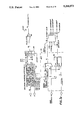
Images


Classifications
-
- G—PHYSICS
- G06—COMPUTING; CALCULATING OR COUNTING
- G06F—ELECTRIC DIGITAL DATA PROCESSING
- G06F13/00—Interconnection of, or transfer of information or other signals between, memories, input/output devices or central processing units
- G06F13/14—Handling requests for interconnection or transfer
- G06F13/20—Handling requests for interconnection or transfer for access to input/output bus
- G06F13/28—Handling requests for interconnection or transfer for access to input/output bus using burst mode transfer, e.g. direct memory access DMA, cycle steal
-
- G—PHYSICS
- G06—COMPUTING; CALCULATING OR COUNTING
- G06F—ELECTRIC DIGITAL DATA PROCESSING
- G06F12/00—Accessing, addressing or allocating within memory systems or architectures
- G06F12/02—Addressing or allocation; Relocation
- G06F12/06—Addressing a physical block of locations, e.g. base addressing, module addressing, memory dedication
- G06F12/0646—Configuration or reconfiguration
- G06F12/0684—Configuration or reconfiguration with feedback, e.g. presence or absence of unit detected by addressing, overflow detection
-
- G—PHYSICS
- G06—COMPUTING; CALCULATING OR COUNTING
- G06F—ELECTRIC DIGITAL DATA PROCESSING
- G06F13/00—Interconnection of, or transfer of information or other signals between, memories, input/output devices or central processing units
- G06F13/14—Handling requests for interconnection or transfer
- G06F13/16—Handling requests for interconnection or transfer for access to memory bus
- G06F13/1668—Details of memory controller
- G06F13/1694—Configuration of memory controller to different memory types
Definitions
- This invention relates generally to a memory module for an information processing system and, in particular, to a memory module having selectable operating modes including a selectable data bus width and a selectable memory device control signal generation.
- a memory module for an information processing system typically includes a substrate, such as a printed circuit board, a plurality of memory device integrated circuits, such as dynamic random access memories (DRAMS), and associated logic for generating memory timing and control signals, latching data, etc.
- DRAMS dynamic random access memories
- One or more of the memory modules are coupled to a system bus of an information processing system and provide storage of data and instructions for one or more central processing units (CPUs) which are also coupled to the system bus.
- CPUs central processing units
- the memory module(s) may be coupled to the system bus via a memory bus and a memory control unit (MCU), the MCU being interposed between the system bus and the memory bus.
- MCU memory control unit
- the system bus normally includes a data bus having a predetermined number of signal lines for defining a width of the bus.
- a data bus may have 8, 16, 32, 64 or more signal lines for conveying an equal number of data bits.
- Modern, high performance systems are generally characterized by a data bus width of 64 bits (double-word) or 128 bits (quad-word).
- the system bus normally also includes an address bus for defining data storage address locations within the memory module(s).
- the number of signal lines which comprise the address bus is directly related to the number of address storage locations which may be directly addressed by the the bus. For example, 20 address signal lines can directly address approximately one million address locations. Modern systems may have 28 or more address signal lines.
- the address bus is provided as a discrete bus while for other types of systems the address bus is time shared, or multiplexed, with all or a portion of the data bus.
- the multiplexed signal lines can convey an address during a first portion of a system bus cycle and convey data relating to the address during a second portion of the system bus cycle.
- the system bus typically also includes a number of control signal lines such as memory read and write strobes, clock and bus cycle timing signal lines, etc.
- DRAM devices are available in a number of operating configurations including page mode and static column mode.
- a row address is applied to the device, a row address strobe (RAS*) signal is asserted, a column address is applied and a column address strobe (CAS*) signal is asserted such that a particular address location within the DRAM is selected.
- the device is repetitively accessed in the page mode by incrementing the column address and reasserting CAS* without incurring the overhead of also changing the row address and reasserting RAS*.
- a conventional page mode type of DRAM page mode operation includes repetitive assertions of CAS*.
- the DRAM includes circuitry which detects transitions of the column address signals.
- this type of device the requirement of repetitively asserting CAS* is eliminated in that applying a new column address, with CAS* remaining asserted, is sufficient to initiate a device read or write access cycle to the selected address.
- static column operation results in a faster access cycle in that set-up and hold times associated with CAS* are eliminated.
- DRAM devices have differing timing and control signal generation requirements which generally preclude conventional memory modules from operating with both types of devices. That is, conventional memory modules are typically designed to work with one type of device or the other. In that DRAM devices are in great demand and adequate supplies of a given type of device are not always readily available it can be seen that a memory module having the ability to operate with more than one type of DRAM device without modification is a desirable feature.
- the memory unit includes a bus coupling the memory unit to the memory control unit by a plurality of signal lines.
- the memory unit further includes a latch for receiving and storing an address from the bus, a first memory plane for storing information units associated with an odd address, a second memory plane for storing information units associated with an even address, an input latch for receiving from the bus an information unit associated with a received address and output latches for storing, prior to transmission to the bus, a stored information unit associated with a received address.
- the memory unit further includes logic, responsive to a state of a first bus signal line, for enabling the output latches to (a) simultaneously transmit to the bus an information unit from both the first and the second memory planes, or (b) sequentially transmit to the bus an information unit from one of the memory planes followed by an information unit from the other one of the memory planes.
- Each of the memory planes further has an associated counter for storing and incrementing a portion of a column address, the counters being responsive to a bus signal asserted by the memory control unit.
- a bus signal asserted by the memory control unit Up to 256 double-word write accesses or up to 128 quad-word read accesses can be achieved by supplying an initial address and thereafter toggling the bus signal to increment the counters.
- page mode type of DRAMs toggling the bus signal also results in a deassertion and a reassertion of the CAS signal.
- static column type of DRAMs the transition of the address counter outputs is sufficient to cause the DRAMs to begin a new access cycle.
- the memory unit of the invention furthermore provides status signals to the memory control unit including a match signal to indicate that a particular memory unit lies within a range of addresses associated with a provided address and a signal which indicates, when asserted, that static column type of DRAMs are installed upon the memory unit asserting the match signal.
- FIG. 1 is a block diagram of a portion of an information processing system showing a MCU coupled to a number of MUs via a MEMBUS;
- FIG. 2a shows in greater detail one embodiment of the MEMBUS of FIG. 1;
- FIG. 2b shows in greater detail a second embodiment of the MEMBUS of FIG. 1;
- FIG. 2c is a block diagram partly in schematic form, which shows in greater detail the control and timing block 26;
- FIG. 3 the relative orientation of FIGS. 3a, 3b and 3c;
- FIGS. 3a, 3b and 3c are each a portion of a simplified block diagram of the MU of the invention.
- FIG. 4 shows in greater detail certain signals of the MU control bus which is a part of the MEMBUS;
- FIG. 5 shows the signal timing for a double-word MU read operation
- FIG. 6 shows the signal timing for a quad-word MU read operation
- FIG. 6a shows an octal-word read cycle for a double-word width system
- FIG. 6b shows a quad-word read cycle for a double-word width system
- FIG. 7 shows the signal timing for a consecutive quad-word MU read operation
- FIG. 8 shows the signal timing for a byte write operation
- FIG. 9 shows the signal timing for a word/double-word write operation
- FIG. 10 shows the signal timing for a consecutive double-word write operation
- FIG. 11 shows the signal timing for a refresh operation
- FIG. 12 shows the signal timing for a refresh operation including a correction
- FIGS. 13a, 13b and 13c are timing diagrams which illustrate the operation of certain signal lines in different configurations of systems.
- System 10 includes a system bus 12 which couples together a number of bus connections including a memory control unit (MCU) 14.
- MCU memory control unit
- Other bus connections such as a CPU (not shown) provide data to the MCU 14 to be written to memory and also receive data read from memory.
- MEMBUS memory bus
- MUs memory units
- MU0MU7 up to eight MUs 18 (MU0-MU7) can be coupled to the MCU 14 via the MEMBUS 16.
- MEMBUS 16 can be seen to comprise two groups of signal lines including a control bus 20 and a data/address bus 22.
- the control bus 20 can be seen to comprise a plurality of signal lines which are sourced by, for example, a memory interface state machine 24 on the MCU 14.
- the memory interface state machine 24 is responsive to a memory access type opcode which is generated by a bus connection and which is sent over the system bus 12 to the MCU 14.
- the opcode defines a particular type of memory access such as a double-word read, a quad-word read, or a word or double-word write.
- the memory interface state machine 24 decodes the opcode and provides the necessary sequence of control signals to the MUs 18.
- a control and timing logic block 26 on the MU 18 receives the control bus 20 signals and, in synchronism with a memory clock (MEMCLK), generates a plurality of internal timing signals for the MU 18.
- the MU 18 can be further seen to include an odd double-word memory plane 28 and an even double-word memory plane 30.
- Planes 28 and 30 are each comprised of a plurality of memory devices which are preferably DRAMS. In the illustrated embodiment each of the planes 28 and 30 is differentiated into an upper and a lower half, each half having eight megabytes of storage organized as one megabyte by 78 bits. Sixty-four of the bits comprise a data double-word and the remaining 14 bits are error detection and correction (ECC) syndrome bits.
- ECC error detection and correction
- a memory address is provided to the planes 28 and 30 from the MCU 14 via a memory address driver 32 which is controlled by a drive address (DRVADR) signal generated by the memory interface state machine 24.
- DRVADR drive address
- the address bits are time multiplexed with a portion of the data bus 22.
- the address is latched in the MU 18 by an address input latch 34 and is provided to two address logic blocks 36 and 38, block 36 being associated with the odd double-word plane 28 and block 38 being associated with the even double-word plane 30.
- the memory interface state machine 24 For a write type of memory access, generates a drive data signal (DRVDAT) which drives, via a driver 39, the contents of an internal data path to the MEMBUS data/address bus 22.
- DDVDAT drive data signal
- a single write cycle may be up to 64 data bits (double-word) in width (plus ECC syndrome bits) while a single read access cycle may be up to 128 bits (quad-word) in width.
- the data driven to MDB0 ⁇ 00:77> is received by a data input latch 40 and is provided therefrom to one of the planes 28 and 30 while a write strobe (WSTB) signal is gated to the proper plane for writing.
- WSTB write strobe
- the data outputs from the planes 28 and/or 30 are provided to a data output latch 42 which drives the data/address bus 22.
- the data is received by a latch 44 on the MCU 14 and is provided therefrom to the internal MCU 14 data path.
- the MU 18 also includes a unit select logic block 46 which decodes a portion of the address input to determine whether a particular MU 18 is selected by (matches) the provided address.
- the unit select logic block 46 returns a signal MATCH* to the MCU 14 if a MATCH condition is detected.
- FIG. 2b illustrates the MU 18 in use with a MCU 14' which employs a single 78-bit data/address bus 22.
- the MU 18 includes an additional data latch 48 which is employed to multiplex the data output of the odd double-word plane 28 onto the MDB0 (00:77) bus 22.
- the operation of latch 48 is controlled by the control and timing block 26, as are the other latches and logic previously described, which in turn is responsive to particular ones of the control bus 20 signals as will be described.
- the MU 18 provides either a first data bus width or a second data bus width which is twice that of the first width.
- the MU 18 can be employed with at least the two types of MCU 14 and 14' without requiring circuit changes to be made to the MU 18.
- FIGS. 2c, 3a and 3b there is shown the MU 18 in greater detail. Specifically there is shown in FIG. 2c the control and timing block 26 in greater detail and in FIGS. 3a and 3b the internal address and data paths and also the board address match logic.
- the MDB0 ⁇ 00:77> bus is coupled to the address input latch 34 which can further be seen is comprised of a buffer 34a and latch 34b.
- the address input latch 34 which can further be seen is comprised of a buffer 34a and latch 34b.
- bits of address are applied on the MDB0 signal lines and are latched by latch 34b for application to the even double-word address logic 38 and the odd double-word address logic 36.
- the odd double-word address logic 36 can be seen to include a counter 36a and a row and column select multiplexer 36b.
- the even double-word address logic 38 is comprised of an adder 38a, a counter 38b and a row and column select logic 38c.
- Counters 36a and 38b are each an eight-bit counter which are preloaded with eight bits of the latched column address (LA(20-27)).
- Counters 36a and 38b each have an input (INCADDR) for incrementing the counter value by a value of one for accessing consecutive double-words from their respective memory planes.
- Bit 29 is applied to the control block 26 and selects within a memory plane the even or odd word while bit 28 is employed for selecting either the even or the odd memory planes 28 and 30 for access.
- LA ⁇ 26-29> may equal 0100 2 .
- both planes 28 and 30 are provided with an address having LSBs of 0001.sub.(2).
- both planes retrieve data from the provided address. After a first memory read access the counters 36a and 38b are both incremented by the assertion of INCADDR such that both have a value of 0010.sub.(2) for accessing the next consecutive double-word.
- both counters will again have an initial value of 0001.sub.(2).
- the adder 38a first adds a one to the even memory plane 30 column address before the address is stored in counter 38b such that the even double-word plane counter 38b does not fall behind the odd plane counter 36a. That is, the odd double-word plane is accessed at address 0001.sub.(2) while the even double-word plane is initially accessed at address 001.sub.(2). After incrementing both counters 36a and 38b the next odd plane address from counter 36a is 0010 while the next even plane address from counter 38b is 0011.sub.(2).
- the multiplexers 36b and 38c each apply two sets of 11 bits of address to the DRAM double-word memory planes 28 and 30 which, in conjunction with the appropriate RAS* and CAS* signals, are strobed into the memories for selecting a particular address location.
- the assertion of the RAM COL* signal switches the output of multiplexers 36b and 38c from the row address to the column address provided by the counters 36a and 38b, respectively. It should be realized that ten of these eleven address bits are strobed directly into the one megabyte DRAMs and that in other embodiments of the invention that more or less than this number of bits are provided depending on the density of the individual memory devices. For example, if four megbyte DRAMs are employed all eleven of the address bits are used.
- Data input latch 40 is employed during memory write cycles and is a 64 data bit, plus 14 ECC syndrome bit width latch, the outputs of which are applied to the data input terminals of the memory devices of the two memory planes 28 and 30.
- Each of the double-word memory planes 28 and 30 has a data output latch associated therewith, namely the 78-bit latches L4 42a and L6 42b.
- Latches L4 42a and L6 42b are employed when the MU 18 is utilized with the MCU 14 of FIG. 2a for simultaneously providing up to 128 bits, or one quad-word of data, for memory read cycles.
- Each of the latches L4 42a and L6 42b has an associated 78-bit output driver 50 and 52, respectively, coupled to an output thereof for driving the MDB0 and MDB1 buses, respectively.
- the odd double-word memory plane 28 further has the 78-bit latch L5 48 coupled to its output, the latch 48 having an output coupled to the input of the even double-word memory plane driver 50.
- the latch 48 is utilized to multiplex the output of the odd double-word memory plane 28 on to the MDBO ⁇ 00:77> bus.
- the MU 18 further includes a memory logic array (MLA) 54 which is utilized to determine if a particular bus address selects the MU 18 for a read or write cycle. A base address input is compared to a portion of the address from buffer 34a. If the address is determined to be within a range of addresses which correspond to a particular MU 18 an output of a comparator 56 asserts the MATCH* signal which is provided on the memory bus 16 to the MU 14.
- the MLA 54 further functions to provide a base address output to a next consecutive MU 18 in a manner which is disclosed in copending patent application Ser. No. 07/179 162 filed Apr. 8, 1988, now U.S. Pat. No. 4,913,966, issued Jul. 24, 1990.
- FIG. 4 shows in greater detail the memory control bus 20 of FIG. 2a and FIG. 2b.
- the function of the various signals shown in FIG. 4 are better understood by also referring to the timing diagrams of FIGS. 5-12 which show a variety of memory access types.
- the MEMCLOCK* signal is provided from the MCU 14 to the MU 18 and establishes a reference clock signal for the MU 18.
- the CLOSE* signal captures and latches the address appearing on MDBO ⁇ 02:31> at the beginning of a memory operation. As can be seen in FIG. 5, the CLOSE signal is asserted when the memory address is set up on MDB0 at the beginning of a memory access cycle. CLOSE remains asserted until the end of the memory access cycle.
- DTOUT* and DTIN* are provided from the MCU 14 and convey a four bit code to the MU 18.
- the four bit code provided by the DTOUT* and DTIN* signals are employed during read and write operations and is used by the MU 18 to enable the MU 18 buffers and other circuitry for writing to the MU 18 or for reading from the MU 18.
- Table 1 illustrates the use of DTOUT* and DTIN* in conjunction with other signals.
- the row address strobe (RAS*) signal is generated by the MCU 14 and is provided via the control and timing block 26 to the memory devices on the MU 18 to strobe in the row address provided from the multiplexers 36b and 38c.
- the column address strobe (CAS*) is generated by the MU 18 for both read and write access cycles. It should be noted that if the memory unit has static column type DRAMs that CAS* remains asserted during multiple memory access cycles.
- a write strobe (WRSTB*) is generated by the MCU 14 for write-type access cycles and is provided, as can be seen in FIG. 8, substantially coincidentally with the provision of write data on the memory bus 16.
- the control bus 20 includes a BWD* signal and a BDWD* signal.
- the BWD* signal is utilized for all memory accesses of a double-word or greater in width.
- the BDWD* signal is used for all memory accesses which are a quad-word in width.
- BDW* and BDWD* control via the control and timing block 26, which of the memory planes 28 and 30 receive RAS*, CAS* and WRSTRB*.
- For a byte or word write cycle (FIGS. 8 and 9) neither BDW* or BDWD* is generated, the memory plane section being accomplished by LA ⁇ 29>.
- LA ⁇ 29> is ignored and BDW* and LA ⁇ 28> control the memory plane selection.
- LA 29 and LA 28 are ignored and BWD* and BDWD* control memory plane selection.
- LA 28 controls the proper sequencing of the planes.
- a refresh (RFRSH*) signal is periodically generated by the MCU 14 in order to initiate a refresh cycle on the MU 18.
- the refresh cycle is performed as a read operation, having both RAS* and CAS* asserted, which enables the MCU 14 to read the data at the refresh location and to perform error "sniffing" and correction if necessary.
- FIG. 12 it can be seen that the refresh cycle indicated a bit in error and that corrected data is written back to the MU 18 during the time that the WSTRB* signal is asserted.
- the MATCHED* signal is returned to the MCU 14 only by the MU 18 which generates a matched condition with the MCU 14 provided address. Furthermore, a STATMATCH* signal is provided back the MCU 14 simultaneously with the provision of the MATCHED* signal only for those MU 18s which employ static column DRAMs.
- the STATMATCH* signal can be utilized by the MCU 14 to modify its internal timing in that the STATMATCH* signal being asserted generally indicates that a faster memory access is possible.
- the AHCMATCH* signal is output from the matched MU to the MCU 14; the assertion of AHCMATCH* being caused by the generation of MATCHED* and also a MU jumper or switch which indicates that DRAMs having a specified speed are installed.
- AHCMATCH* is a status signal to the MCU 14 which indicates that the MU is adding one half of a MEMCLK cycle to the memory access to accommodate the timing requirements of the DRAMs. For example, if faster access DRAMs are installed the jumper may not be set and AHCMATCH* is therefore not asserted.
- page mode DRAMs are characterized as requiring multiple assertion of CAS* in order to accomplish consecutive memory accesses.
- the NEXT* signal is utilized for page mode DRAMs in order to cause successive assertions of the CAS* signal.
- the counters 38b and 36a can also be incremented by NEXT* between accesses in order to increment the column address. Therefore, the assertion of the NEXT* signal is employed for multiple read and write type of accesses for page mode DRAMs as well as for static-column DRAMs. However, the assertion of NEXT*, for static column DRAMs, increments the address but does not affect CAS*.
- the Next Enable (NEXTENA*) signal is employed, when asserted, to enable the gating of the NEXT* signal onto the MU 18.
- the NEXTENA* signal can be hard wired on the control bus 20 to either an enabling or a disabling logic state.
- the assertion of NEXTENA* indicates that the MU 18 is coupled to an MCU which generates the signal NEXT* to perform multiple memory accesses.
- a quad data bus (QDBS*) signal which specifies to the MU 18 whether the MEMBUS 16 is a double-word (64 bit) or a quad-word (128 bit) type bus.
- the QDBS* signal can be tied to a logic signal on the MEMBUS 16.
- the MU 18 is notified that it is installed in a quad-word bus type of system.
- the MU 18 is notified that it is installed in a double-word bus type of system and that latch L5 48 is required to multiplex the odd double-word plane 28 output onto the MDB0 bus.
- the NEXTENA* signal enables the generation of an ENABLECAS* signal via gate 62, F/F 64 and gate 66.
- the output of F/F 64 is a registered NEXT* (RNEXT*) signal.
- the ENABLECAS* signal is asserted when NEXT* is asserted by the MCU 14 in conjunction with the NEXTENA* signal and also when the MU 18 provides a signal STATCOL which indicates that static column DRAMS are not installed.
- the ENABLECAS* signal is provided to a Memory Array Control (MAC) block 68 for enabling the assertion of certain CAS ⁇ 0:7> signals to the memory planes 28 and 30.
- MAC Memory Array Control
- FIGS. 13a, 13b and 13c are timing diagrams which illustrate the operation of these signal lines in different configurations of systems.
- FIG. 13a shows a double-word width data bus system having page mode DRAMs and a maximum operation size of an octal-word read.
- FIG. 13b illustrates a quad-word width data bus system having static column DRAMs.
- FIG. 13c illustrates a quad-word width data bus system having page mode DRAMs.
- the terminal rising edge of the increment address (INCADDR) signal is a don't care state in that the operation has already ended.
- MAC 68 includes a number of Control Bus 20 inputs including WRST*, BWD*, BDWD*, DTIN* and DTOUT*. The state of these signals is decoded by the MAC 68 for generating the required ones of the memory strobe signals.
- a portion of the MAC 68 is a Latch Control 72 which decodes certain of the input signals for generating various latch controlling outputs, including L4CONT, L5CONT and L6CONT.
- L4CONT L5CONT
- L6CONT L4CONT
- QDBS* QDBS* is asserted then L5CONT is not generated, QDBS* indicating that the MU 18 is installed in a quad-word wide MEMBUS 16 system.
- L5CONT is generated for multiplexing the odd double-word memory plane output to the even double-word bus, namely MDB0 ⁇ 00:77>.
- the MAC 68 also controls the generation of the ADD signal to adder 38a to initially add a one to the even double-word counter 38b as previously described.
- Control Bus 20 in conjunction with Control and Timing block 26 enables up to 128 consecutive quad-word read cycles or up to 256 consecutive double-word write cycles. These consecutive read or write accesses are accomplished by providing the initial address and thereafter repetitively asserting the NEXT* signal from the MCU 14.
- the MEMCLOCK signal provides a reference clock, cycles of which are shown numbered consecutively.
- the address from MCU 14 is stable at the rising edge of MEMCLOCK 2 and the CLOSE* and RAS* signals are asserted.
- the BWD* signal is also asserted for indicating that a double-word operation is in progress.
- a row address is provided by the appropriate multiplexer 36b or 38c and at rising edge of MEMCLOCK3 the row address is strobed into the DRAMs by the RAM RAS* signal.
- the multiplexer thereafter switches to the column address provided from the associated counter 36a or 38b and RAM CAS* is generated at MEMCLOCK4 for strobing into the addressed DRAMs the column address.
- RAM CAS* is generated at MEMCLOCK4 for strobing into the addressed DRAMs the column address.
- the MCU 14 asserts DTOUT* to enable output drivers etc., thereby enabling the MU 18 output data path, including the appropriate data latch.
- Data read from the addressed memory plane is driven to the appropriate MDB bus 22.
- MEMCLOCK6 the MCU 14 latches the data and at the end of MEMCLOCK6 CLOSE* is deasserted, thereby terminating the MCU 14 access.
- FIG. 6 illustrates a quad-word read cycle wherein the QD bus is used, this cycle being similar in operation to the double-word read of FIG. 5.
- both the MDB0 and MDB1 buses are employed.
- the DBWD* signal is asserted coincidentally with BWD* for indicating that both double-word memory planes 28 and 30 are being accessed.
- the diagram of FIG. 6 illustrates the quad-word MEMBUS 16 configuration, the QDBS* signal (not shown) being asserted from the backplane. If the double-word MEMBUS 16' of FIG. 2b is employed the latch L5 48 is employed to provide the odd memory plane double-word to MDB0 in the MEMCLOCK8.
- FIG. 6a illustrates an octal-word read cycle
- FIG. 6b a quad-word read for the double-word width bus case.
- the RCLOSE* signal is a registered CLOSE* signal.
- FIG. 7 illustrates two consecutive quad-word read operations, it being realized that up to 128 quad-word reads may be accomplished in such manner.
- the memory access proceeds up to MEMCLOCK5 in a manner as previously described.
- the NEXT* signal is asserted to indicate that a second quad-word read cycle is desired.
- the rising edge of NEXT* at MEMCLOCK6 causes the generation of the INCADDR signal thereby incrementing the column address counters 36a and 38b. If static column type DRAMs are installed RAM CAS* remains asserted and the change of state of the column address initiates the next DRAM access cycle.
- RAM CAS* is deasserted, as indicated in dashed outline, for one MEMCLOCK cycle after which RAM CAS* is once more asserted to initiate the second DRAM access.
- DTOUT* is asserted a second time in order to retrieve the second quad-word of data. If more than two quad-words of data are required each quad-word is accessed by the assertion of NEXT* with an assertion of DTOUT*.
- FIG. 8 illustrates a byte write operation. This type of write operation is achieved by initially performing a word or a double-word read of the memory plane having the byte to be written, merging within the MCU 14 the byte into the word or double-word and writing back the merged word or double-word to the memory plane. This portion of the cycle is accomplished from MEMCLOCK1 to MEMCLOCK7. At MEMCLOCK7 DTIN* is asserted and at MEMCLOCK8 WRSTRB* is asserted. The double-word containing the newly merged byte of data is also driven to MDB0 ⁇ 00:77> at MEMCLOCK8. It can be noted that RAM CAS* remains asserted throughout this read-modify-write type of access.
- FIG. 9 illustrates a word or a double-word type of write cycle.
- BWD* is not asserted for a word write cycle but is asserted, as shown in dashed outline, at MEMCLOCK2 for the double-word case.
- FIG. 10 illustrates a consecutive double-word write access.
- a first double-word is driven to MDB0 ⁇ 00:77> during MEMCLOCK4 in conjunction with WRSTB*.
- This first double-word is stored in either the odd or even memory plane depending on the state of the address (LA 28) driven during MEMCLOCK2 and MEMCLOCK3.
- a second double-word is driven at MEMCLOCK6 along with WRSTRB* and the second double-word is stored in the memory plane not previously written.
- NEXT* is asserted at MEMCLOCK7, the rising edge of which at MEMCLOCK8 causes the column address to increment via counters 36a and 38b.
- the third and fourth double-words are driven, along with an associated WRSTB*, during MEMCLOCK8-12 for storage within the memory planes.
- Both BWD* and BDWD* are asserted at MEMCLOCK2 and DTIN* is asserted at MEMCLOCK3. If an additional double-word write access were required NEXT* would be reasserted at MEMCLOCK11 with CLOSE*, RAS* and DTIN* remaining asserted.
- FIG. 11 illustrates a refresh operation which is periodically initiated by the MCU 14 for refreshing the DRAMs.
- the refresh operation is performed as a word or double-word read operation similar to that of FIG. 5.
- the word or double-word of data, including ECC syndrome bits, which is read from the refreshed location is processed by error detection and correction circuitry within the MCU 18 to detect and correct single bit errors or to detect multiple bit errors.
- the RFRSH* signal is asserted by the MCU 14 in conjunction with CLOSE*, RAS* and BWD*.
- FIG. 11 shows the case where no errors are detected.
- FIG. 12 illustrates a refresh operation wherein a bit of the word or double-word is found to be in error.
- the operation of this refresh cycle during MEMCLOCK1-8 is identical to that of FIG. 11.
- the error is corrected by the MCU 14 and a word or double-word write cycle is initiated at MEMCLOCK8 in order to write the corrected word or double-word back into the memory location from which it was read.
- This MCU 14 initiated write cycle can be seen to be identical to that of FIG. 9 with BWD* asserted.
Abstract
Description
                                  TABLE 1
__________________________________________________________________________
DESCRIPTION OF DTOUT* AND DTIN*
DTOUT*
      DTIN*
          QDBS*
               BDWD*
                    LA28
__________________________________________________________________________
0     X   0    1    0   Enables latch & driver outputs (42a & 50)
                        to send data to MCU for memory reads
0     X   0    1    1   Enables latch & driver outputs (42b & 52)
                        to send read data to MCU for memory reads
0     X   0    0    X   Enables latch & driver outputs (42a & 50 & 42b &
                        52) to send read data to MCU for memory reads
0     0   1    X    X   Enables latch & driver outputs (48 & 50)
                        to send read data to MCU for memory reads
0     1   l    X    X   Enables latch & driver outputs (42a & 50)
                        to send read data to MCU for memory reads
1     0   X    X    X   Enables buffer & latch outputs (34a & 40)
                        to drive data into MU array for writes
1     l   X    X    X   No buffer or latch outputs enabled
__________________________________________________________________________
Claims (7)
Priority Applications (5)
| Application Number | Priority Date | Filing Date | Title |
|---|---|---|---|
| US07/786,327 US5261073A (en) | 1989-05-05 | 1991-10-31 | Method and apparatus for providing memory system status signals |
| US08/092,628 US6021477A (en) | 1989-05-05 | 1993-07-15 | Multiple mode memory module |
| US09/401,335 US6499093B2 (en) | 1989-05-05 | 1999-09-21 | Multiple mode memory module |
| US09/400,131 US6523100B2 (en) | 1989-05-05 | 1999-09-21 | Multiple mode memory module |
| US09/854,555 US6564308B2 (en) | 1989-05-05 | 2001-05-15 | Multiple mode memory module |
Applications Claiming Priority (2)
| Application Number | Priority Date | Filing Date | Title |
|---|---|---|---|
| US07/348,318 US5307469A (en) | 1989-05-05 | 1989-05-05 | Multiple mode memory module |
| US07/786,327 US5261073A (en) | 1989-05-05 | 1991-10-31 | Method and apparatus for providing memory system status signals |
Related Parent Applications (1)
| Application Number | Title | Priority Date | Filing Date |
|---|---|---|---|
| US07/348,318 Division US5307469A (en) | 1989-05-05 | 1989-05-05 | Multiple mode memory module |
Related Child Applications (1)
| Application Number | Title | Priority Date | Filing Date |
|---|---|---|---|
| US08/092,628 Continuation US6021477A (en) | 1989-05-05 | 1993-07-15 | Multiple mode memory module |
Publications (1)
| Publication Number | Publication Date |
|---|---|
| US5261073A true US5261073A (en) | 1993-11-09 |
Family
ID=26995642
Family Applications (4)
| Application Number | Title | Priority Date | Filing Date |
|---|---|---|---|
| US07/786,327 Expired - Lifetime US5261073A (en) | 1989-05-05 | 1991-10-31 | Method and apparatus for providing memory system status signals |
| US08/092,628 Expired - Lifetime US6021477A (en) | 1989-05-05 | 1993-07-15 | Multiple mode memory module |
| US09/400,131 Expired - Fee Related US6523100B2 (en) | 1989-05-05 | 1999-09-21 | Multiple mode memory module |
| US09/401,335 Expired - Fee Related US6499093B2 (en) | 1989-05-05 | 1999-09-21 | Multiple mode memory module |
Family Applications After (3)
| Application Number | Title | Priority Date | Filing Date |
|---|---|---|---|
| US08/092,628 Expired - Lifetime US6021477A (en) | 1989-05-05 | 1993-07-15 | Multiple mode memory module |
| US09/400,131 Expired - Fee Related US6523100B2 (en) | 1989-05-05 | 1999-09-21 | Multiple mode memory module |
| US09/401,335 Expired - Fee Related US6499093B2 (en) | 1989-05-05 | 1999-09-21 | Multiple mode memory module |
Country Status (1)
| Country | Link |
|---|---|
| US (4) | US5261073A (en) |
Cited By (10)
| Publication number | Priority date | Publication date | Assignee | Title |
|---|---|---|---|---|
| US5327539A (en) * | 1991-02-26 | 1994-07-05 | Fujitsu Limited | Access processing system in information processor |
| US5611054A (en) * | 1994-03-18 | 1997-03-11 | Intel Corporation | Method and apparatus for decoding and recoding of addresses |
| US5664168A (en) * | 1993-11-29 | 1997-09-02 | Motorola, Inc. | Method and apparatus in a data processing system for selectively inserting bus cycle idle time |
| US5854944A (en) * | 1996-05-09 | 1998-12-29 | Motorola, Inc. | Method and apparatus for determining wait states on a per cycle basis in a data processing system |
| US5872992A (en) * | 1995-08-24 | 1999-02-16 | Motorola, Inc. | System and method for avoiding bus contention on a multiplexed bus by providing a time period subsequent to a read operation |
| WO2002015356A1 (en) * | 2000-08-16 | 2002-02-21 | Chen Han Ping | Memory access conversion mechanism |
| DE19644495C2 (en) * | 1995-10-25 | 2002-07-18 | Hyundai Electronics Ind | storage device |
| US6505282B1 (en) * | 1994-11-30 | 2003-01-07 | Intel Corporation | Method and apparatus for determining memory types of a multi-type memory subsystem where memory of the different types are accessed using column control signals with different timing characteristics |
| US6523100B2 (en) | 1989-05-05 | 2003-02-18 | Samsung Electronics Co., Ltd. | Multiple mode memory module |
| US8127275B1 (en) * | 2007-04-18 | 2012-02-28 | Parasoft Corporation | System and method for recording the state of variables and objects when running unit tests |
Families Citing this family (18)
| Publication number | Priority date | Publication date | Assignee | Title |
|---|---|---|---|---|
| US5790888A (en) * | 1996-08-12 | 1998-08-04 | Seeq Technology, Inc. | State machine for selectively performing an operation on a single or a plurality of registers depending upon the register address specified in a packet |
| FR2766573B1 (en) * | 1997-07-28 | 1999-09-24 | Commissariat Energie Atomique | PROCESS FOR THE SCREENING AND / OR PROGNOSIS OF CANCER BY DETECTION OF A PROTEIN OF THE TUBULIN TYROSINATION-DETYROSINATION CYCLE AND ITS APPLICATIONS |
| EP1185920A4 (en) * | 1998-11-09 | 2005-07-06 | Broadcom Corp | Mixed-signal single-chip integrated system electronics for magnetic hard disk drives |
| US6480948B1 (en) * | 1999-06-24 | 2002-11-12 | Cirrus Logic, Inc. | Configurable system memory map |
| US6839820B1 (en) * | 2000-07-20 | 2005-01-04 | Silicon Graphics, Inc. | Method and system for controlling data access between at least two memory arrangements |
| US7143185B1 (en) * | 2000-08-29 | 2006-11-28 | Advanced Micro Devices, Inc. | Method and apparatus for accessing external memories |
| US6785856B1 (en) | 2000-12-07 | 2004-08-31 | Advanced Micro Devices, Inc. | Internal self-test circuit for a memory array |
| US6684353B1 (en) | 2000-12-07 | 2004-01-27 | Advanced Micro Devices, Inc. | Reliability monitor for a memory array |
| US7346331B2 (en) * | 2001-09-30 | 2008-03-18 | Harrow Products, Llc | Power management for locking system |
| US7289764B2 (en) * | 2001-09-30 | 2007-10-30 | Harrow Products, Llc | Cardholder interface for an access control system |
| US20030103472A1 (en) * | 2001-09-30 | 2003-06-05 | Ronald Taylor | RF wireless access control for locking system |
| US20030074936A1 (en) * | 2001-09-30 | 2003-04-24 | Fred Conforti | Door wireless access control system including reader, lock, and wireless access control electronics including wireless transceiver |
| US20030096607A1 (en) * | 2001-09-30 | 2003-05-22 | Ronald Taylor | Maintenance/trouble signals for a RF wireless locking system |
| KR100518532B1 (en) * | 2002-04-27 | 2005-10-04 | 삼성전자주식회사 | Method and apparatus for transmitting command signal and address signal selectively |
| US7747286B2 (en) * | 2004-01-20 | 2010-06-29 | Harrow Products Llc | Wireless access control system with energy-saving piezo-electric locking |
| US20060059963A1 (en) * | 2004-01-20 | 2006-03-23 | Harrow Products Llc | Wireless access control system including wireless exit kit (''WEXK'') with panic bar |
| US7339837B2 (en) * | 2004-05-18 | 2008-03-04 | Infineon Technologies Ag | Configurable embedded processor |
| US9417091B2 (en) * | 2013-05-13 | 2016-08-16 | The Johns Hopkins University | System and method for determining and correcting field sensors errors |
Citations (16)
| Publication number | Priority date | Publication date | Assignee | Title |
|---|---|---|---|---|
| US4309754A (en) * | 1979-07-30 | 1982-01-05 | International Business Machines Corp. | Data interface mechanism for interfacing bit-parallel data buses of different bit width |
| JPS5715271A (en) * | 1980-06-30 | 1982-01-26 | Toshiba Corp | Memory device |
| US4366539A (en) * | 1980-10-31 | 1982-12-28 | Honeywell Information Systems Inc. | Memory controller with burst mode capability |
| US4371928A (en) * | 1980-04-15 | 1983-02-01 | Honeywell Information Systems Inc. | Interface for controlling information transfers between main data processing systems units and a central subsystem |
| US4467443A (en) * | 1979-07-30 | 1984-08-21 | Burroughs Corporation | Bit addressable variable length memory system |
| US4509113A (en) * | 1982-02-02 | 1985-04-02 | International Business Machines Corporation | Peripheral interface adapter circuit for use in I/O controller card having multiple modes of operation |
| US4580214A (en) * | 1982-03-02 | 1986-04-01 | Hitachi, Ltd. | Memory control system |
| US4631671A (en) * | 1981-11-26 | 1986-12-23 | Hitachi, Ltd. | Data processing system capable of transferring single-byte and double-byte data under DMA control |
| US4716545A (en) * | 1985-03-19 | 1987-12-29 | Wang Laboratories, Inc. | Memory means with multiple word read and single word write |
| US4727475A (en) * | 1984-05-18 | 1988-02-23 | Frederick Kiremidjian | Self-configuring modular computer system with automatic address initialization |
| US4763302A (en) * | 1985-06-21 | 1988-08-09 | Mitsubishi Denki Kabushiki Kaisha | Alternatively addressed semiconductor memory array |
| US4839856A (en) * | 1985-12-23 | 1989-06-13 | Kabushiki Kaisha Toshiba | Memory access control circuit |
| US4849937A (en) * | 1984-12-14 | 1989-07-18 | Mitsubishi Denki Kabushiki Kaisha | Digital delay unit with interleaved memory |
| US4943907A (en) * | 1987-05-08 | 1990-07-24 | Colorado Memory Systems, Inc. | Speed controller for recording and playback apparatus |
| US4947366A (en) * | 1987-10-02 | 1990-08-07 | Advanced Micro Devices, Inc. | Input/output controller incorporating address mapped input/output windows and read ahead/write behind capabilities |
| US5029124A (en) * | 1988-05-17 | 1991-07-02 | Digital Equipment Corporation | Method and apparatus for providing high speed parallel transfer of bursts of data |
Family Cites Families (12)
| Publication number | Priority date | Publication date | Assignee | Title |
|---|---|---|---|---|
| US3872452A (en) | 1974-04-17 | 1975-03-18 | Ibm | Floating addressing system and method |
| US4001790A (en) | 1975-06-30 | 1977-01-04 | Honeywell Information Systems, Inc. | Modularly addressable units coupled in a data processing system over a common bus |
| US4281392A (en) | 1979-05-01 | 1981-07-28 | Allen-Bradley Company | Memory circuit for programmable machines |
| US4751671A (en) | 1983-02-14 | 1988-06-14 | Prime Computer, Inc. | Size configurable data storage system |
| US4787060A (en) | 1983-03-31 | 1988-11-22 | Honeywell Bull, Inc. | Technique for determining maximum physical memory present in a system and for detecting attempts to access nonexistent memory |
| US4725945A (en) * | 1984-09-18 | 1988-02-16 | International Business Machines Corp. | Distributed cache in dynamic rams |
| US4744025A (en) | 1985-05-02 | 1988-05-10 | Digital Equipment Corporation | Arrangement for expanding memory capacity |
| US4780916A (en) | 1987-05-11 | 1988-11-01 | Sutton Bernard S | Tub seat massager |
| US4980850A (en) * | 1987-05-14 | 1990-12-25 | Digital Equipment Corporation | Automatic sizing memory system with multiplexed configuration signals at memory modules |
| US5301278A (en) * | 1988-04-29 | 1994-04-05 | International Business Machines Corporation | Flexible dynamic memory controller |
| GB2226667B (en) | 1988-12-30 | 1993-03-24 | Intel Corp | Self-identification of memory |
| US5261073A (en) | 1989-05-05 | 1993-11-09 | Wang Laboratories, Inc. | Method and apparatus for providing memory system status signals |
-
1991
- 1991-10-31 US US07/786,327 patent/US5261073A/en not_active Expired - Lifetime
-
1993
- 1993-07-15 US US08/092,628 patent/US6021477A/en not_active Expired - Lifetime
-
1999
- 1999-09-21 US US09/400,131 patent/US6523100B2/en not_active Expired - Fee Related
- 1999-09-21 US US09/401,335 patent/US6499093B2/en not_active Expired - Fee Related
Patent Citations (16)
| Publication number | Priority date | Publication date | Assignee | Title |
|---|---|---|---|---|
| US4467443A (en) * | 1979-07-30 | 1984-08-21 | Burroughs Corporation | Bit addressable variable length memory system |
| US4309754A (en) * | 1979-07-30 | 1982-01-05 | International Business Machines Corp. | Data interface mechanism for interfacing bit-parallel data buses of different bit width |
| US4371928A (en) * | 1980-04-15 | 1983-02-01 | Honeywell Information Systems Inc. | Interface for controlling information transfers between main data processing systems units and a central subsystem |
| JPS5715271A (en) * | 1980-06-30 | 1982-01-26 | Toshiba Corp | Memory device |
| US4366539A (en) * | 1980-10-31 | 1982-12-28 | Honeywell Information Systems Inc. | Memory controller with burst mode capability |
| US4631671A (en) * | 1981-11-26 | 1986-12-23 | Hitachi, Ltd. | Data processing system capable of transferring single-byte and double-byte data under DMA control |
| US4509113A (en) * | 1982-02-02 | 1985-04-02 | International Business Machines Corporation | Peripheral interface adapter circuit for use in I/O controller card having multiple modes of operation |
| US4580214A (en) * | 1982-03-02 | 1986-04-01 | Hitachi, Ltd. | Memory control system |
| US4727475A (en) * | 1984-05-18 | 1988-02-23 | Frederick Kiremidjian | Self-configuring modular computer system with automatic address initialization |
| US4849937A (en) * | 1984-12-14 | 1989-07-18 | Mitsubishi Denki Kabushiki Kaisha | Digital delay unit with interleaved memory |
| US4716545A (en) * | 1985-03-19 | 1987-12-29 | Wang Laboratories, Inc. | Memory means with multiple word read and single word write |
| US4763302A (en) * | 1985-06-21 | 1988-08-09 | Mitsubishi Denki Kabushiki Kaisha | Alternatively addressed semiconductor memory array |
| US4839856A (en) * | 1985-12-23 | 1989-06-13 | Kabushiki Kaisha Toshiba | Memory access control circuit |
| US4943907A (en) * | 1987-05-08 | 1990-07-24 | Colorado Memory Systems, Inc. | Speed controller for recording and playback apparatus |
| US4947366A (en) * | 1987-10-02 | 1990-08-07 | Advanced Micro Devices, Inc. | Input/output controller incorporating address mapped input/output windows and read ahead/write behind capabilities |
| US5029124A (en) * | 1988-05-17 | 1991-07-02 | Digital Equipment Corporation | Method and apparatus for providing high speed parallel transfer of bursts of data |
Cited By (10)
| Publication number | Priority date | Publication date | Assignee | Title |
|---|---|---|---|---|
| US6523100B2 (en) | 1989-05-05 | 2003-02-18 | Samsung Electronics Co., Ltd. | Multiple mode memory module |
| US5327539A (en) * | 1991-02-26 | 1994-07-05 | Fujitsu Limited | Access processing system in information processor |
| US5664168A (en) * | 1993-11-29 | 1997-09-02 | Motorola, Inc. | Method and apparatus in a data processing system for selectively inserting bus cycle idle time |
| US5611054A (en) * | 1994-03-18 | 1997-03-11 | Intel Corporation | Method and apparatus for decoding and recoding of addresses |
| US6505282B1 (en) * | 1994-11-30 | 2003-01-07 | Intel Corporation | Method and apparatus for determining memory types of a multi-type memory subsystem where memory of the different types are accessed using column control signals with different timing characteristics |
| US5872992A (en) * | 1995-08-24 | 1999-02-16 | Motorola, Inc. | System and method for avoiding bus contention on a multiplexed bus by providing a time period subsequent to a read operation |
| DE19644495C2 (en) * | 1995-10-25 | 2002-07-18 | Hyundai Electronics Ind | storage device |
| US5854944A (en) * | 1996-05-09 | 1998-12-29 | Motorola, Inc. | Method and apparatus for determining wait states on a per cycle basis in a data processing system |
| WO2002015356A1 (en) * | 2000-08-16 | 2002-02-21 | Chen Han Ping | Memory access conversion mechanism |
| US8127275B1 (en) * | 2007-04-18 | 2012-02-28 | Parasoft Corporation | System and method for recording the state of variables and objects when running unit tests |
Also Published As
| Publication number | Publication date |
|---|---|
| US6021477A (en) | 2000-02-01 |
| US20020023192A1 (en) | 2002-02-21 |
| US6523100B2 (en) | 2003-02-18 |
| US20020144049A1 (en) | 2002-10-03 |
| US6499093B2 (en) | 2002-12-24 |
Similar Documents
| Publication | Publication Date | Title |
|---|---|---|
| US5261073A (en) | Method and apparatus for providing memory system status signals | |
| US5307469A (en) | Multiple mode memory module | |
| US7082491B2 (en) | Memory device having different burst order addressing for read and write operations | |
| US5301278A (en) | Flexible dynamic memory controller | |
| EP0549139B1 (en) | Programmable memory timing | |
| EP0348113B1 (en) | Programmable burst apparatus and technique | |
| US4803621A (en) | Memory access system | |
| US5265231A (en) | Refresh control arrangement and a method for refreshing a plurality of random access memory banks in a memory system | |
| US5329629A (en) | Apparatus and method for reading, writing, and refreshing memory with direct virtual or physical access | |
| EP0339224A2 (en) | Memory controller | |
| JPS6259820B2 (en) | ||
| EP0307945B1 (en) | Memory control apparatus for use in a data processing system | |
| US4903197A (en) | Memory bank selection arrangement generating first bits identifying a bank of memory and second bits addressing identified bank | |
| US5265053A (en) | Main memory DRAM interface | |
| US5553270A (en) | Apparatus for providing improved memory access in page mode access systems with pipelined cache access and main memory address replay | |
| US5901298A (en) | Method for utilizing a single multiplex address bus between DRAM, SRAM and ROM | |
| US6564308B2 (en) | Multiple mode memory module | |
| US4964037A (en) | Memory addressing arrangement | |
| US6292867B1 (en) | Data processing system | |
| US5684979A (en) | Method and means for initializing a page mode memory in a computer | |
| US5524228A (en) | Memory control circuit for reducing the number of row address signals | |
| JPS62249246A (en) | Memory system | |
| JPS63126047A (en) | Memory control system | |
| JPH0823844B2 (en) | Memory controller |
Legal Events
| Date | Code | Title | Description |
|---|---|---|---|
| STCF | Information on status: patent grant |
Free format text: PATENTED CASE |
|
| AS | Assignment |
Owner name: CONGRESS FINANCIAL CORPORATION (NEW ENGLAND), MASS Free format text: SECURITY INTEREST;ASSIGNOR:WANG LABORATORIES, INC.;REEL/FRAME:006932/0047 Effective date: 19931220 |
|
| AS | Assignment |
Owner name: WANG LABORATORIES, INC., MASSACHUSETTS Free format text: RELEASE OF SECURITY INTEREST IN AND REASSIGNMENT OF U.S. PATENTS AND PATENT APPLICATIONS;ASSIGNOR:CONGRESS FINANCIAL CORPORATION (NEW ENGLAND);REEL/FRAME:007341/0041 Effective date: 19950130 |
|
| AS | Assignment |
Owner name: BT COMMERCIAL CORPORATION (AS AGENT), NEW YORK Free format text: SECURITY INTEREST;ASSIGNOR:WANG LABORATORIES, INC.;REEL/FRAME:007377/0072 Effective date: 19950130 |
|
| AS | Assignment |
Owner name: BT COMMERICAL CORPORATION, NEW YORK Free format text: SECURITY AGREEMENT;ASSIGNOR:WANG LABORATORIES, INC.;REEL/FRAME:008246/0001 Effective date: 19960828 |
|
| FEPP | Fee payment procedure |
Free format text: PAYOR NUMBER ASSIGNED (ORIGINAL EVENT CODE: ASPN); ENTITY STATUS OF PATENT OWNER: LARGE ENTITY |
|
| FPAY | Fee payment |
Year of fee payment: 4 |
|
| AS | Assignment |
Owner name: SAMSUNG ELECTRONICS CO., LTD., KOREA, REPUBLIC OF Free format text: ASSIGNMENT OF ASSIGNORS INTEREST;ASSIGNOR:WANG LABORATORIES, INC.;REEL/FRAME:008744/0555 Effective date: 19970829 |
|
| FEPP | Fee payment procedure |
Free format text: PAYER NUMBER DE-ASSIGNED (ORIGINAL EVENT CODE: RMPN); ENTITY STATUS OF PATENT OWNER: LARGE ENTITY Free format text: PAYOR NUMBER ASSIGNED (ORIGINAL EVENT CODE: ASPN); ENTITY STATUS OF PATENT OWNER: LARGE ENTITY |
|
| FPAY | Fee payment |
Year of fee payment: 8 |
|
| FPAY | Fee payment |
Year of fee payment: 12 |