US4947102A - Feedback loop gain compensation for a switched resistor regulator - Google Patents
Feedback loop gain compensation for a switched resistor regulator Download PDFInfo
- Publication number
- US4947102A US4947102A US07/269,194 US26919488A US4947102A US 4947102 A US4947102 A US 4947102A US 26919488 A US26919488 A US 26919488A US 4947102 A US4947102 A US 4947102A
- Authority
- US
- United States
- Prior art keywords
- control voltage
- signal
- pulse
- nonlinear
- switched resistor
- Prior art date
- Legal status (The legal status is an assumption and is not a legal conclusion. Google has not performed a legal analysis and makes no representation as to the accuracy of the status listed.)
- Expired - Lifetime
Links
- 239000003990 capacitor Substances 0.000 claims description 4
- 238000010586 diagram Methods 0.000 description 5
- 230000000737 periodic effect Effects 0.000 description 2
- 230000000694 effects Effects 0.000 description 1
- 230000003071 parasitic effect Effects 0.000 description 1
- 230000000087 stabilizing effect Effects 0.000 description 1
Images

Classifications
-
- G—PHYSICS
- G05—CONTROLLING; REGULATING
- G05F—SYSTEMS FOR REGULATING ELECTRIC OR MAGNETIC VARIABLES
- G05F1/00—Automatic systems in which deviations of an electric quantity from one or more predetermined values are detected at the output of the system and fed back to a device within the system to restore the detected quantity to its predetermined value or values, i.e. retroactive systems
- G05F1/10—Regulating voltage or current
- G05F1/625—Regulating voltage or current wherein it is irrelevant whether the variable actually regulated is ac or dc
- G05F1/63—Regulating voltage or current wherein it is irrelevant whether the variable actually regulated is ac or dc using variable impedances in series with the load as final control devices
- G05F1/648—Regulating voltage or current wherein it is irrelevant whether the variable actually regulated is ac or dc using variable impedances in series with the load as final control devices being plural resistors among which a selection is made
Definitions
- This invention relates to switched resistor regulators. More specifically, this invention relates to controlling switched resistor regulators so that control feedback loop gain does not vary excessively with changes in operating voltage.
- a switched resistor regulator is a type of power supply regulator, characterized by switching a resistor into and out of electrical connection between a power source and a load.
- SRRs and their operation are fully disclosed in U.S. Pat. No. 4,668,906, issued May 26, 1987 in the name of inventor John P. Ekstrand, and assigned to the same assignee. Some applications and improvements with respect to SRRs are disclosed in U.S. Pat. No. 4,719,404, issued Jan. 12, 1988 in the name of inventor John P.
- a typical SRR employs a pulse-width modulator ("PWM") to generate a pulse train, which is applied to the switch for switching the resistor into and out of electrical connection.
- PWM pulse-width modulator
- a feedback loop is employed to assure that the pulse train generated by the PWM switches the resistor at a duty cycle which preserves the indicated operating voltage and/or current.
- a problem arises when it is desired to operate the SRR at operating conditions which are widely varying. Because the SRR has a nonlinear response to changes in control voltage, the gain from the control voltage to the output voltage and/or current may differ at different operating conditions. This difference can be substantial when the operating conditions are substantially different.
- the feedback control loop employed by the SRR for stabilizing the duty cycle of the resistor will be subject to a problem. While it is not difficult to adjust for operating parameters (e.g. speed of response and reduction of ripple) which are optimum at any fixed operating point, it is difficult to select operating parameters which will be optimum (or nearly so) at operating voltages which are widely varying, precisely because the gain of the feedback control loop differs at different operating voltages. This effect is well known in the art of feedback regulative control. Inability to select those operating parameters which are preferred can degrade the performance of systems whose power is being supplied by the SRR.
- operating parameters e.g. speed of response and reduction of ripple
- a switched resistor regulator is constructed with a pulse-width modulator whose duty cycle response is nonlinear with changes in operating voltage. Specifically, the response of the pulse-width modulator is made to increase nonlinearly with small changes in input control voltage, so as to compensate for the nonlinear nature of the switched resistor regulator.
- the pulse-width modulator is altered by comparing the input control voltage with a nonlinear reference signal, rather than the substantially linear reference signal which is used in prior art pulse-width modulators.
- the nonlinear reference signal may be generated by a nonlinear reference voltage circuit, such as an RC charging circuit, or such as a D/A converter controlled by a clocked programmable microprocessor.
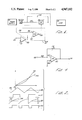
- FIG. 1 shows a block diagram of a feedback loop employed for control of a switched resistor regulator.
- FIG. 2 shows several voltage response diagrams for switched resistor regulators.
- FIG. 3 shows a circuit diagram of a pulsed-width modulator for a switched resistor regulator.
- FIG. 4 shows a gain change element
- FIG. 5 shows an alternative embodiment of the invention including a D/A converter.
- FIG. 1 shows a block diagram of a switched resistor regulator ("SRR") and a feedback loop employed for control of that SRR.
- SRR switched resistor regulator
- one configuration 102 of a SRR comprises a resistor 104, a switch 106, and a capacitor 108, and is electrically connected in series between an unregulated power supply 110 and filter 112, and a load 114.
- a voltage proportional to the current received by the load 114 appears at node 116, and is further transmitted to a first input 118 of a differential amplifier 120.
- a second input 122 of the differential amplifier 120 is set to a desired set point voltage at node 124.
- An output 126 of the differential amplifier 120 generates a control voltage, which is transmitted to an input 130 of a comparator 132.
- the comparator 132 compares this control voltage to a reference signal applied at node 134 and transmitted to another input 136 of the comparator 132, and generates an output pulse train at an output node 144, which is transmitted to and controls switch 106.
- output node 144 may comprise a plurality of nodes, e.g. nodes 144a-b, for control of a plurality of switches 106.
- the PWM 150 may comprise the comparator 132, its output 144, and the control voltage 126 and reference signal applied to node 134.
- the PWM 150 may operate to generate a pulse train by comparing its input control voltage with a periodic reference voltage signal.
- the periodic reference signal is substantially linear in known PWMs used in the context of SRRs.
- the reference signal is nonlinear with such nonlinearity selected to compensate for the nonlinearity of the SRR. This is more fully disclosed with respect to FIG. 2.
- FIG. 2 shows several response curves for PWMs of SRRs.
- Curve 202 shows the response of a PWM, in which pulse width is linear with control voltage.
- Curve 208 shows a reference signal 212 which is compared with a control voltage 216 so as to generate a train of pulses of varying width; curve 210 shows a resultant pulse train. Because the reference signal 212 rises and falls substantially linearly, the pulse width will change substantially linearly with control voltage 216, as shown in curve 202.
- Curve 218 shows the response of a PWM in which the response has been altered to be nonlinear with control voltage. It will become clear to one of ordinary skill in the art that curve 218 may have other useful shapes in an embodiment of the invention, and that such would remain within the concept and scope of the invention.
- Curve 224 shows a control voltage 228 which is compared with a reference signal 230 so as to generate a train of pulses of varying width; curve 226 shows a resultant pulse train. Because the reference signal 230 rises and falls nonlinearly, a pulse generated in response to a control voltage 228 will vary in width substantially nonlinearly, as shown in curve 218.
- FIG. 3 shows a circuit diagram of one configuration of a switched resistor regulator and control circuitry.
- a clock 302 generates a clock signal on path 304.
- the clock signal on path 304 is transmitted to a divide-by-two circuit 306, which generates a half-clock signal on a pair of paths 308a-b.
- the half-clock signal on paths 308a-b is transmitted to a buffer 310, which generates a pair of out-of-phase pulse signals on signal paths 312a-b respectively.
- the out-of-phase pulse signals on paths 312a-b are transmitted to a pair of reset-on-pulse circuits 314a-b respectively, each of which discharges a capacitor 320a-b respectively.
- the capacitors are recharged via timing resistors 318a-b respectively.
- control voltage is applied at an input 140, and compared by two comparators 322a-b to produce pulses at node 144a-b.
- FIG. 4 shows a gain change element.
- a gain change element may be inserted in place of the wire 152 in FIG. 1.
- the control voltage from output 126 is passed through a resistor 402 and transmitted to a first input 404 of an operational amplifier 406.
- a second input 408 of the operational amplifier 406 is grounded.
- the first input 404 and an output 410 of the operational amplifier 406 are connected by a variable resistor 412.
- the output 410 is connected to input 130 of the comparator 132.
- variable resistor 412 may comprise any element which performs the function of a variable resistor. Examples include a potentiometer, a D/A converter, a FET, a light-sensitive cell or phototransistor, or any equivalent circuit.
- FIG. 5 shows an alternative embodiment of the invention including D/A converter (154). All like circuit elements from FIG. 1 are represented by the same reference numerals.
Abstract
Description
Claims (15)
Priority Applications (1)
| Application Number | Priority Date | Filing Date | Title |
|---|---|---|---|
| US07/269,194 US4947102A (en) | 1988-11-08 | 1988-11-08 | Feedback loop gain compensation for a switched resistor regulator |
Applications Claiming Priority (1)
| Application Number | Priority Date | Filing Date | Title |
|---|---|---|---|
| US07/269,194 US4947102A (en) | 1988-11-08 | 1988-11-08 | Feedback loop gain compensation for a switched resistor regulator |
Publications (1)
| Publication Number | Publication Date |
|---|---|
| US4947102A true US4947102A (en) | 1990-08-07 |
Family
ID=23026200
Family Applications (1)
| Application Number | Title | Priority Date | Filing Date |
|---|---|---|---|
| US07/269,194 Expired - Lifetime US4947102A (en) | 1988-11-08 | 1988-11-08 | Feedback loop gain compensation for a switched resistor regulator |
Country Status (1)
| Country | Link |
|---|---|
| US (1) | US4947102A (en) |
Cited By (9)
| Publication number | Priority date | Publication date | Assignee | Title |
|---|---|---|---|---|
| US5369472A (en) * | 1992-12-04 | 1994-11-29 | Xerox Corporation | Microprocessor controlled high voltage power supply |
| US5444610A (en) * | 1993-10-22 | 1995-08-22 | Diversified Technologies, Inc. | High-power modulator |
| US5627459A (en) * | 1993-04-19 | 1997-05-06 | Fujitsu Limited | DC/DC converter |
| US5689176A (en) * | 1996-08-07 | 1997-11-18 | Deloy; Jeff J. | Power factor/harmonics correction circuitry and method thereof |
| US5710413A (en) * | 1995-03-29 | 1998-01-20 | Minnesota Mining And Manufacturing Company | H-field electromagnetic heating system for fusion bonding |
| US5883797A (en) * | 1997-06-30 | 1999-03-16 | Power Trends, Inc. | Parallel path power supply |
| US6043636A (en) * | 1997-10-20 | 2000-03-28 | Diversified Technologies, Inc. | Voltage transient suppression |
| US6054847A (en) * | 1998-09-09 | 2000-04-25 | International Business Machines Corp. | Method and apparatus to automatically select operating voltages for a device |
| CN100511076C (en) * | 2003-03-28 | 2009-07-08 | 大动力公司 | Method and system for current sharing among a plurality of power modules |
Citations (5)
| Publication number | Priority date | Publication date | Assignee | Title |
|---|---|---|---|---|
| SU265255A1 (en) * | Б. А. Лапин | METHOD OF STABILIZATION OF OUTPUT VOLTAGE | ||
| US4237405A (en) * | 1978-03-10 | 1980-12-02 | Lear Siegler, Inc. | Method and apparatus for conserving energy |
| US4668906A (en) * | 1985-07-11 | 1987-05-26 | Ekstrand John P | Switched resistor regulator |
| US4719404A (en) * | 1985-07-11 | 1988-01-12 | Spectra-Physics, Inc. | Switched resistor regulator with linear dissipative regulator |
| US4814966A (en) * | 1985-07-11 | 1989-03-21 | Spectra-Physics, Inc. | Shunt switched resistor regulator with diode snubber |
-
1988
- 1988-11-08 US US07/269,194 patent/US4947102A/en not_active Expired - Lifetime
Patent Citations (5)
| Publication number | Priority date | Publication date | Assignee | Title |
|---|---|---|---|---|
| SU265255A1 (en) * | Б. А. Лапин | METHOD OF STABILIZATION OF OUTPUT VOLTAGE | ||
| US4237405A (en) * | 1978-03-10 | 1980-12-02 | Lear Siegler, Inc. | Method and apparatus for conserving energy |
| US4668906A (en) * | 1985-07-11 | 1987-05-26 | Ekstrand John P | Switched resistor regulator |
| US4719404A (en) * | 1985-07-11 | 1988-01-12 | Spectra-Physics, Inc. | Switched resistor regulator with linear dissipative regulator |
| US4814966A (en) * | 1985-07-11 | 1989-03-21 | Spectra-Physics, Inc. | Shunt switched resistor regulator with diode snubber |
Cited By (10)
| Publication number | Priority date | Publication date | Assignee | Title |
|---|---|---|---|---|
| US5369472A (en) * | 1992-12-04 | 1994-11-29 | Xerox Corporation | Microprocessor controlled high voltage power supply |
| US5627459A (en) * | 1993-04-19 | 1997-05-06 | Fujitsu Limited | DC/DC converter |
| US5444610A (en) * | 1993-10-22 | 1995-08-22 | Diversified Technologies, Inc. | High-power modulator |
| US5646833A (en) * | 1993-10-22 | 1997-07-08 | Diversified Technologies, Inc. | Apparatus and method for deriving power for switching a switch from voltage across the switch |
| US5710413A (en) * | 1995-03-29 | 1998-01-20 | Minnesota Mining And Manufacturing Company | H-field electromagnetic heating system for fusion bonding |
| US5689176A (en) * | 1996-08-07 | 1997-11-18 | Deloy; Jeff J. | Power factor/harmonics correction circuitry and method thereof |
| US5883797A (en) * | 1997-06-30 | 1999-03-16 | Power Trends, Inc. | Parallel path power supply |
| US6043636A (en) * | 1997-10-20 | 2000-03-28 | Diversified Technologies, Inc. | Voltage transient suppression |
| US6054847A (en) * | 1998-09-09 | 2000-04-25 | International Business Machines Corp. | Method and apparatus to automatically select operating voltages for a device |
| CN100511076C (en) * | 2003-03-28 | 2009-07-08 | 大动力公司 | Method and system for current sharing among a plurality of power modules |
Similar Documents
| Publication | Publication Date | Title |
|---|---|---|
| US4988942A (en) | Switched resistor regulator control when transfer function includes discontinuity | |
| US4325021A (en) | Regulated switching apparatus | |
| US4504776A (en) | Power saving regulated light emitting diode circuit | |
| US5315164A (en) | Adaptive clock duty cycle controller | |
| US4315106A (en) | Apparatus for regulating current supplied to a telephone line signal of the type employed in digital telephone systems | |
| US4810948A (en) | Constant-voltage regulated power supply circuit | |
| US5084666A (en) | Switchable output voltage converter | |
| US6885177B2 (en) | Switching regulator and slope correcting circuit | |
| US6519167B1 (en) | PWM controller with single-cycle response | |
| JPH01161512A (en) | Dual-input low dropout voltage regulator | |
| US4806873A (en) | Laser diode driving circuit | |
| US4947102A (en) | Feedback loop gain compensation for a switched resistor regulator | |
| US8093882B2 (en) | Low heat dissipation I/O module using direct drive buck converter | |
| US5089768A (en) | Power source device with control of voltage change speed | |
| EP0280170A2 (en) | Generator of periodic signals, in particular for switch-mode power supplies | |
| US6381154B1 (en) | PWM nonlinear controller with a single cycle response and a non resettable integrator | |
| EP0662747B1 (en) | A DC/DC converter for outputting multiple signals | |
| EP0443250B1 (en) | A general purpose low cost digital amplitude regulator | |
| US3996531A (en) | Oscillator circuit whose frequency is voltage controllable which contains a comparator | |
| JP2803151B2 (en) | Power supply | |
| JPH05115173A (en) | Variable dc power supply | |
| JP2841085B2 (en) | Switching voltage regulator with stabilized loop gain | |
| KR100438979B1 (en) | Circuit of analog current output | |
| US5504380A (en) | Method and apparatus for controlling a current generator | |
| US4546270A (en) | Sample and hold droop compensation circuit |
Legal Events
| Date | Code | Title | Description |
|---|---|---|---|
| AS | Assignment |
Owner name: SPECTRA-PHYSICS, INC., CALIFORNIA Free format text: ASSIGNMENT OF ASSIGNORS INTEREST.;ASSIGNORS:EKSTRAND, JOHN P.;HOLSINGER, KEVIN;REEL/FRAME:005047/0142 Effective date: 19890209 |
|
| STCF | Information on status: patent grant |
Free format text: PATENTED CASE |
|
| AS | Assignment |
Owner name: SPECTRA-PHYSICS LASERS, INC. A DE CORPORATION, CA Free format text: ASSIGNMENT OF ASSIGNORS INTEREST.;ASSIGNOR:SPECTRA-PHYSICS, INC.;REEL/FRAME:005751/0193 Effective date: 19910604 |
|
| FEPP | Fee payment procedure |
Free format text: PAYOR NUMBER ASSIGNED (ORIGINAL EVENT CODE: ASPN); ENTITY STATUS OF PATENT OWNER: LARGE ENTITY |
|
| REMI | Maintenance fee reminder mailed | ||
| FPAY | Fee payment |
Year of fee payment: 4 |
|
| SULP | Surcharge for late payment | ||
| FPAY | Fee payment |
Year of fee payment: 8 |
|
| REMI | Maintenance fee reminder mailed | ||
| FPAY | Fee payment |
Year of fee payment: 12 |
|
| REMI | Maintenance fee reminder mailed |