US20030191786A1 - Computer method and apparatus for division and square root operations using signed digit - Google Patents
Computer method and apparatus for division and square root operations using signed digit Download PDFInfo
- Publication number
- US20030191786A1 US20030191786A1 US10/419,454 US41945403A US2003191786A1 US 20030191786 A1 US20030191786 A1 US 20030191786A1 US 41945403 A US41945403 A US 41945403A US 2003191786 A1 US2003191786 A1 US 2003191786A1
- Authority
- US
- United States
- Prior art keywords
- digit
- signal
- carry
- partial remainder
- signed
- Prior art date
- Legal status (The legal status is an assumption and is not a legal conclusion. Google has not performed a legal analysis and makes no representation as to the accuracy of the status listed.)
- Granted
Links
- 238000000034 method Methods 0.000 title abstract description 6
- 230000001419 dependent effect Effects 0.000 claims abstract description 34
- 230000001934 delay Effects 0.000 abstract description 3
- 230000007704 transition Effects 0.000 description 17
- 238000010586 diagram Methods 0.000 description 12
- 230000008901 benefit Effects 0.000 description 2
- 230000000644 propagated effect Effects 0.000 description 2
- 238000001342 constant potential amperometry Methods 0.000 description 1
- 230000006870 function Effects 0.000 description 1
- 239000013598 vector Substances 0.000 description 1
Images


Classifications
-
- G—PHYSICS
- G06—COMPUTING; CALCULATING OR COUNTING
- G06F—ELECTRIC DIGITAL DATA PROCESSING
- G06F7/00—Methods or arrangements for processing data by operating upon the order or content of the data handled
- G06F7/38—Methods or arrangements for performing computations using exclusively denominational number representation, e.g. using binary, ternary, decimal representation
- G06F7/48—Methods or arrangements for performing computations using exclusively denominational number representation, e.g. using binary, ternary, decimal representation using non-contact-making devices, e.g. tube, solid state device; using unspecified devices
- G06F7/52—Multiplying; Dividing
- G06F7/535—Dividing only
-
- G—PHYSICS
- G06—COMPUTING; CALCULATING OR COUNTING
- G06F—ELECTRIC DIGITAL DATA PROCESSING
- G06F7/00—Methods or arrangements for processing data by operating upon the order or content of the data handled
- G06F7/38—Methods or arrangements for performing computations using exclusively denominational number representation, e.g. using binary, ternary, decimal representation
- G06F7/48—Methods or arrangements for performing computations using exclusively denominational number representation, e.g. using binary, ternary, decimal representation using non-contact-making devices, e.g. tube, solid state device; using unspecified devices
- G06F7/4824—Methods or arrangements for performing computations using exclusively denominational number representation, e.g. using binary, ternary, decimal representation using non-contact-making devices, e.g. tube, solid state device; using unspecified devices using signed-digit representation
-
- G—PHYSICS
- G06—COMPUTING; CALCULATING OR COUNTING
- G06F—ELECTRIC DIGITAL DATA PROCESSING
- G06F7/00—Methods or arrangements for processing data by operating upon the order or content of the data handled
- G06F7/38—Methods or arrangements for performing computations using exclusively denominational number representation, e.g. using binary, ternary, decimal representation
- G06F7/48—Methods or arrangements for performing computations using exclusively denominational number representation, e.g. using binary, ternary, decimal representation using non-contact-making devices, e.g. tube, solid state device; using unspecified devices
- G06F7/50—Adding; Subtracting
- G06F7/505—Adding; Subtracting in bit-parallel fashion, i.e. having a different digit-handling circuit for each denomination
- G06F7/506—Adding; Subtracting in bit-parallel fashion, i.e. having a different digit-handling circuit for each denomination with simultaneous carry generation for, or propagation over, two or more stages
- G06F7/508—Adding; Subtracting in bit-parallel fashion, i.e. having a different digit-handling circuit for each denomination with simultaneous carry generation for, or propagation over, two or more stages using carry look-ahead circuits
-
- G—PHYSICS
- G06—COMPUTING; CALCULATING OR COUNTING
- G06F—ELECTRIC DIGITAL DATA PROCESSING
- G06F7/00—Methods or arrangements for processing data by operating upon the order or content of the data handled
- G06F7/38—Methods or arrangements for performing computations using exclusively denominational number representation, e.g. using binary, ternary, decimal representation
- G06F7/48—Methods or arrangements for performing computations using exclusively denominational number representation, e.g. using binary, ternary, decimal representation using non-contact-making devices, e.g. tube, solid state device; using unspecified devices
- G06F7/544—Methods or arrangements for performing computations using exclusively denominational number representation, e.g. using binary, ternary, decimal representation using non-contact-making devices, e.g. tube, solid state device; using unspecified devices for evaluating functions by calculation
- G06F7/552—Powers or roots, e.g. Pythagorean sums
- G06F7/5525—Roots or inverse roots of single operands
-
- G—PHYSICS
- G06—COMPUTING; CALCULATING OR COUNTING
- G06F—ELECTRIC DIGITAL DATA PROCESSING
- G06F9/00—Arrangements for program control, e.g. control units
- G06F9/06—Arrangements for program control, e.g. control units using stored programs, i.e. using an internal store of processing equipment to receive or retain programs
- G06F9/30—Arrangements for executing machine instructions, e.g. instruction decode
- G06F9/38—Concurrent instruction execution, e.g. pipeline, look ahead
- G06F9/3802—Instruction prefetching
- G06F9/3814—Implementation provisions of instruction buffers, e.g. prefetch buffer; banks
-
- G—PHYSICS
- G06—COMPUTING; CALCULATING OR COUNTING
- G06F—ELECTRIC DIGITAL DATA PROCESSING
- G06F9/00—Arrangements for program control, e.g. control units
- G06F9/06—Arrangements for program control, e.g. control units using stored programs, i.e. using an internal store of processing equipment to receive or retain programs
- G06F9/30—Arrangements for executing machine instructions, e.g. instruction decode
- G06F9/38—Concurrent instruction execution, e.g. pipeline, look ahead
- G06F9/3836—Instruction issuing, e.g. dynamic instruction scheduling or out of order instruction execution
- G06F9/3838—Dependency mechanisms, e.g. register scoreboarding
- G06F9/384—Register renaming
-
- G—PHYSICS
- G06—COMPUTING; CALCULATING OR COUNTING
- G06F—ELECTRIC DIGITAL DATA PROCESSING
- G06F2207/00—Indexing scheme relating to methods or arrangements for processing data by operating upon the order or content of the data handled
- G06F2207/535—Indexing scheme relating to groups G06F7/535 - G06F7/5375
- G06F2207/5352—Non-restoring division not covered by G06F7/5375
Definitions
- the speed of the division or square root operation is dependent on the amount of time it takes to complete one iteration and the total number of iterations required.
- the total number of iterations is dependent on the number of quotient or root mantissa digits required to provide an accurate quotient or root. For example, in floating point division twenty-four mantissa digits are required for single precision and fifty-three mantissa digits are required for double-precision, therefore the time required to generate each of the required quotient digits is critical to the speed of the division operation.
- a root digit and a correction term are computed after examining a current partial remainder.
- the succeeding or partial remainder for the next iteration is computed by subtracting the correction term from the current partial remainder and scaling the result of the subtraction.
- a quotient digit is computed after comparing a current partial remainder and the divisor.
- the partial remainder for the next iteration is computed by subtracting a multiple of the divisor from the current partial remainder and scaling the result of the subtraction.
- a next partial remainder and an output digit is determined by a decoder coupled to an adder, the adder coupled to a scaler.
- the decoder computes the root digit and binary correction term dependent on a number of digits of a partial remainder.
- the partial remainder is stored in signed digit format.
- the adder generates a signed digit result by subtracting the binary correction term from the signed digit partial remainder.
- the scaler computes the next partial remainder dependent on the signed digit result from the adder.
- the signed digit values are selected from a set of digit values.
- the adder computes a carry out bit independent of the carry in bit.
- the scaler computes the next signed digit partial remainder by scaling the current signed digit partial remainder upward.
- a mathematical square root operation is performed by a decoder coupled to an adder, the adder coupled to a scaler.
- the decoder computes the root digit and binary correction term dependent on a number of digits of a partial remainder.
- the partial remainder is stored in signed digit format.
- the adder generates a signed digit result by subtracting the binary correction term from the signed digit partial remainder.
- the scaler computes the next partial remainder dependent on the signed digit result from the adder.
- the signed digit values are selected from a set of digit values.
- the set of digit values may be minus one, zero or one, or minus two, minus one, zero, plus one and plus two or any other set of digit values containing more than two digit values.
- the adder computes a carry out bit independent of the carry in bit.
- the output signals in the adder may be initialized to predetermined voltage levels.
- the scaler computes the next signed digit partial remainder by scaling the current signed digit remainder upward.
- a mathematical division operation is performed by a decoder coupled to an adder, the adder coupled to a scaler.
- the decoder computes the quotient digit and binary correction term dependent on a number of digits of a partial remainder.
- the partial remainder is stored in signed digit format.
- the adder generates a signed digit result by subtracting the binary correction term from the signed digit partial remainder.
- the scaler computes the next partial remainder dependent on the signed digit result from the adder.
- FIG. 1 is a block diagram of a computer system in which the present invention may be used;
- FIG. 2 is a block diagram of the CPU module shown in FIG. 1;
- FIG. 3 is a block diagram of the floating point square root operation in the FBOX shown in FIG. 2;
- FIG. 4 is a block diagram of the adder shown in FIG. 3 showing a number of identical signed digit adders
- FIG. 5 is a block diagram of any of the signed digit adders shown in FIG. 4;
- FIG. 6 is a schematic of one embodiment of the present invention employing the adder of FIG. 5;
- FIG. 7 is a timing diagram for the embodiment shown in FIG. 6;
- FIG. 8 is a block diagram of another embodiment of any of the signed digit adders shown in FIG. 4;
- FIG. 9 is a schematic of another embodiment of the present invention employing the adder of FIG. 8;
- FIGS. 10 A-B are a schematic of yet another embodiment of any of the signed digit adders shown in FIG. 4;
- FIG. 11 is a schematic of an embodiment of a scaler shown in FIG. 3 for use with signed digit adders of the type shown in FIGS. 10 A-B.
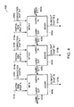
- FIG. 1 is a block diagram of a typical computer system 100 in which the present invention is utilized. Included in the computer system 100 are a Central Processing Unit (“CPU”) module 108 , a memory system 106 and a PCI chip set 110 connected by a processor bus 112 . The PCI chip set 110 is further connected to an Input/Output (“I/O”) system 104 and a co-processor module 102 by a system bus 114 .
- CPU Central Processing Unit
- I/O Input/Output
- FIG. 2 shows the CPU module 108 shown in FIG. 1.
- the CPU module 108 includes a CPU 220 , a backup cache 214 and a processor bus interface logic 216 connected by a private address bus 212 and a private data bus 218 .
- the processor bus interface logic 216 connects the CPU module 108 to the processor bus 112 (FIG. 1).
- the CPU 220 includes a primary cache 208 and a cache control (CBOX) logic 210 .
- the cache control logic (CBOX) 210 controls the primary cache 208 in the CPU 220 and the backup cache 214 .
- CPU 220 further includes logic circuits to enable it to perform operations for the computer system 100 .
- An Instruction Fetch and Decode Unit (IBOX) 202 performs instruction prefetch, decode, branch prediction, instruction issuance and interrupt handling operations.
- An Integer Execution Unit (EBOX) 204 performs mathematical operations on integer values such as, addition, shifting, byte manipulation, and multiplication.
- a Floating Point Execution Unit (FBOX) 200 performs mathematical operations on floating point values such as, square root, division and multiplication.
- a Memory Management Unit (MBOX) 206 performs memory address translation, for example, from virtual memory addresses to physical memory addresses.
- FIG. 3 shows a block diagram of a square root unit 300 located in the Floating Point Execution Unit (FBOX) 200 shown in FIG. 2.
- the square root unit 300 computes a root 324 for a radicand 326 , by computing one root digit 328 per iteration.
- a root digit 328 is computed in the decoder 304 dependent on a current partial remainder 314
- a correction term 316 is computed in the multiplexor 306 .
- a succeeding or next partial remainder 320 is computed by adding the correction term 316 to the current partial remainder 314 in an adder 308 , and scaling the result of the addition 318 in a scaler 310 .
- the time taken for each iteration is dependent on the sum of the speed of each of the decoder 304 , the adder 308 and the scaler 310 .
- the current partial remainder 314 is represented in signed digit format.
- the signed digit format may consist of values selected from the radix-2 set of signed digits ⁇ 1, 0, 1 ⁇ or the radix-4 set of signed digits ⁇ 2, ⁇ 1, 0, 1, 2 ⁇ or any other set of signed digits. Representing the current partial remainder 314 in signed digit format, a redundant format, allows the current partial remainder 314 to be examined quickly in the decoder 304 .
- decoder 304 uses the sign of the most significant non-zero digit, as the sign of the overall current partial remainder 314 . For example, if the four MSBs of the current partial remainder 314 are set to the signed digit values 0, ⁇ 1, 1, ⁇ 1, the current partial remainder 314 is negative because the most significant non-zero digit is ⁇ 1. Accordingly, using signed digit representation reduces the complexity of examining partial remainder 314 , in comparison to methods employing CSAs, where carry and sum vectors must be combined. In turn, the reduced complexity of the examination reduces the total time and thus increases the overall speed of the decoder 304 .
- the number of digits required to be examined by decoder 304 is a function of the correction term's 316 ability to add or subtract from the current partial remainder 314 .
- the preferred embodiment with digit values selected from the radix-2 set ⁇ 1, 0, 1 ⁇ requires the four most significant bits of the current partial remainder 314 to be examined less than four bits may be required in other embodiments.
- the square root unit 300 includes a correction multiplexor 306 .
- the correction multiplexor 306 selects the correction term 316 for the current iteration dependent on the input correction terms 322 and the root digit 328 .
- the adder 308 adds the correction term 316 in binary format to the current partial remainder 314 in signed digit format.
- the result of the addition 318 is in signed digit format.
- the carry value is determined in a manner such that the carry out from a bit position does not depend on the carry in received from the output of the previous, lower order, bit position. This is achieved by satisfying the following equation, for each bit position, in the case with the current partial remainder 314 in signed digit format with digit values selected from the set ⁇ 1, 0, 1 ⁇ :
- A value of the current partial remainder 314 for the given bit position.
- C in value of the Carry_In, for the given bit position.
- C out value of the Carry_Out, for the given bit position.
- S out value of the Sum_Out, for the given bit position.
- the scaler 310 generates the next partial remainder 320 by scaling the result of the addition 318 upward.
- the scaler 310 multiplies the result of the addition 318 by a multiplication factor dependent on the set of correction terms used to reduce the partial remainder.
- the embodiments described in conjunction with FIGS. 6, 9, 10 and 11 use a multiplication factor of two; other factors may be used.
- Multiplying the result of a radix-2 addition 318 by two involves scaler 310 shifting the result of the addition 318 by one digit to generate the next partial remainder 320 .
- Multiplying the result of a radix-4 addition 318 by two is described in conjunction with FIG. 11.
- the square root unit 300 includes a first multiplexor 302 .
- the first multiplexor 302 selects the radicand 326 in binary format as the current partial remainder 314 for the first iteration. In subsequent iterations the next partial remainder 320 is selected as the current partial remainder 314 .
- the correction multiplexor 306 selects the correction term 316 for the current iteration dependent on the input correction terms 322 and the root digit 328 .
- the square root unit 300 described in conjunction with FIG. 3 may be used in any operations requiring the iterative generation of partial remainders such as, cube roots and square roots.
- the square root unit 300 may be used to perform a division operation by computing quotient digits in each cycle instead of root digits.
- the radicand 326 is replaced by a dividend
- the correction terms 322 are replaced by divisor terms
- quotient digits are stored in the register 312 and the resulting root 324 is replaced by a quotient.
- FIG. 4 shows details of the adder 308 of FIG. 3 including an array of signed digit adders 404 a - c .
- the number of signed digit adders 404 a - c is not limited to the three shown in FIG. 4, but rather is dependent on the total number of bits (N) of the correction term 316 and the number of bits (N) of current partial remainder 314 to be subtracted in the adder 308 .
- Each signed digit adder 404 a - c has three inputs and two outputs. The inputs include the signed digit of the correction term 316 a - c , signed digit of the current partial remainder 314 a - c and a Carry_In bit 402 a - c .
- the Carry_In bit 402 a - c is the Carry_Out bit 402 a - c from the adjacent lower order signed digit adder 404 c as illustrated by the horizontal chained arrows in FIG. 4.
- the outputs include the result of the addition 318 a - c and the Carry_Out bit 402 b - d to be input to the adjacent higher order bit signed digit adder 404 b - c.
- FIG. 5 shows an embodiment of the signed digit adder 404 a shown in FIG. 4.
- the current partial remainder 314 a is in signed digit format with digit values selected from the radix-2 set ⁇ 1, 0, 1 ⁇ or the radix-4 set ⁇ 2, ⁇ 1, 0, 1, 2 ⁇ .
- the signed digit adder 404 a adds a current partial remainder 314 a in signed digit format to a correction term digit 316 a in binary format and outputs the result of the addition bit 318 a in signed digit format.
- the signed digit adder 404 a includes a compute carry-out logic 504 , a Correction plus_PR_logic 506 and an Add_Carry_In logic 508 .
- the Compute_Carry_Out logic 504 computes the Carry_Out bit 402 b dependent on the current partial remainder digit 314 a and the correction term digit 316 a .
- the Carry_Out bit 402 b is independent of the Carry_In bit 402 a , and therefore Compute_Carry_Out logic 504 differs from a signed digit adder in a CPA, in which the Carry_Out bit is dependent on the Carry_In bit from the previous signed digit adder.
- the Carry_Out bit 402 b is computed in parallel with the SumInt 510 . Therefore the adder does not have to wait for a carry to propagate as in the case of a CPA adder.
- the Carry_In bit 402 a is added to the SumInt 510 and the Sum_Out digit 318 a is output from the adder. Further Carry_Out bit 402 b is available as a Carry_In bit 402 a to provide the Sum-Out digit 318 b in a succeeding adder 404 b . Therefore the Carry_Out bit 402 b does not have to be added later, as in the case of a CSA adder
- the Correction_plus_PR logic 506 computes the sum of the correction term digit 316 a and the current partial remainder digit 314 a and outputs the SumInt 510 in decoded format.
- the Add_Carry_In logic 508 adds the SumInt 510 and the Carry_In bit 402 a from the previous signed digit adder 404 and outputs a Sum_Out digit 318 a in signed digit format.
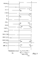
- FIG. 6 shows a schematic for one embodiment of the signed digit adder 404 a shown in FIG. 5, according to the principles of the present invention.
- the current partial remainder digit 314 a is in signed digit format with digit values selected from the set ⁇ 1, 0, 1 ⁇ .
- the Sum Out digit 318 a is also in signed digit format with digit values selected from the set ⁇ 1, 0, 1 ⁇ . The operation of the schematic is described in conjunction with the timing diagram in FIG. 7 and Tables 3, 4 and 5 below.
- the schematic includes NMOS and PMOS transistors.
- Each of the NMOS and PMOS transistors include a gate, source and drain.
- the NMOS and PMOS transistors act as “ON-OFF” switches.
- An NMOS transistor is turned “ON” by applying a high voltage level ‘1’ to the gate relative to the source.
- a PMOS transistor is turned “ON” by applying a low voltage level ‘0’ to the gate relative to the source.
- NMOS transistors are labeled N and PMOS transistors are labeled P in the schematics shown in FIGS. 6, 10 and 11 .
- the schematic of FIG. 6 includes the blocks, Correction_plus_PR logic 506 , Add_Carry_In logic 508 and Compute_Carry_Out logic 504 discussed in FIG. 5.
- the SumInt 510 , Sum-Out digit 318 a , current partial remainder digit 314 a , correction term digit 316 a , Carry-Out bit 402 b and Carry_In bit 402 a shown in FIG. 5 are divided into separate signals in FIG. 6 as follows:
- the current partial remainder digit 314 a in FIG. 5 in signed digit format corresponds to the A_P_H, A_Z_H and A_M_H signals in FIG. 6.
- the correction term digit 316 a shown in FIG. 5 in binary format corresponds to the B_H and the B_L signals in FIG. 6.
- the Carry_Out bit 402 b shown in FIG. 5 in binary format corresponds to the COUT_H and the COUT_L signals in FIG. 6.
- the Sum_Out digit 318 a in FIG. 5 in signed digit format corresponds to the SOUT_P_H, SOUT_Z_H and SOUT_M_H signals in FIG. 6.
- the Carry_In bit 402 a in FIG. 5 in binary format corresponds to the CIN_H and the CIN_L signals in FIG. 6.
- the Sum_Int bits 510 in FIG. 5 corresponds to the SINT_Z_L and SINT_M_L signals.
- the COUT_H, COUT_L, SOUT_P_H, SOUT_Z_H and SOUT_M_H signals are set to pre-defined voltage levels.
- the PRCH_L signal sets the voltage levels through PMOS transistors P 1 -P 4 .
- the PRCH_L signal is set to a low voltage level ‘0’ during a precharge cycle 724.
- Output signals COUT_H and COUT_L are precharged to a high voltage level ‘1’.
- SOUT_Z_H and SOUT_M_H are precharged to a low voltage level ‘0’.
- the operation of the precharge cycle 724 is described for the COUT_H signal in the schematic shown in FIG. 6.
- the PRCH_L signal is initially set to a low voltage level ‘0’.
- the PRCH_L signal is connected to the gate of P 1 .
- P 1 is a PMOS transistor and turns “ON” when a low voltage level ‘0’ is applied to the gate.
- the P 1 's source 604 is connected to a high voltage level ‘1’, and the high voltage level ‘1’ is applied to P 1 's drain which is connected to the COUT_H signal when P 1 is turned “ON”.
- the Carry_Out logic 504 includes NMOS transistors labeled N 9 -N 14 .
- the Carry_Out logic 504 conditionally sets the COUT_H and COUT_L signals to a low voltage level ‘0’ dependent on the voltage levels of the A_P_H, A_Z_H, A_M_H, B_H and B_L signals as shown in Table 3 below.
- Carry_Out logic 504 The operation of the Carry_Out logic 504 is described for the case with current partial remainder digit 314 a set to logic level ‘0’ and correction term digit 316 a set to logic level ‘1’ in conjunction with FIG. 6 and the Add-Cycle 726 in FIG. 7 .
- A_Z_H signal is set to a high voltage level ‘1’ as shown at voltage level transition 700 in Add-Cycle 726 in FIG. 7.
- the gate of N 10 is set to a high voltage level ‘1’.
- N 10 is switched “ON” and the drain of N 10 is set to a low voltage level ‘0’.
- the B_H signal is set to a high voltage level ‘1’ as shown in voltage level transition 702 in FIG. 7.
- this sets the gate of transistor N 14 to a high voltage level ‘1’.
- N 14 is switched on “ON” and provides a low voltage level ‘0’ at the drain of N 14 as shown at voltage level transition 706 in FIG. 7.
- the COUT_L signal connected to the drain of N 14 is set to a low voltage level ‘0’.
- the A_Z_H signal is set to a low voltage level ‘0’ at voltage transition 712 turning N 10 “OFF” in FIG. 6.
- the B_H signal is set to a low voltage at voltage level transition 714 in FIG. 7 turning N 14 “OFF” in FIG. 6.
- the COUT_L signal is set to a high voltage level ‘1’ at voltage transition level 718 in FIG. 7. It can be seen from the schematic that the Carry_Out bit 402 b value is computed within a maximum of two NMOS transistor delays, for example, N 14 and N 10 in the case described above. It may be also be computed within one transistor delay, for example, N 12 .
- the Correction plus_PR logic 506 operates in parallel to the Carry_Out logic 504 .
- the Correction_plus PR logic 506 sets the SINT_Z_L and SINT_M_L signals to a low voltage level ‘0’ or a high voltage level ‘1’ dependent on the voltage levels of the A_P_H, A_Z_H, A_M_H, B_H and B_L signals as shown in Table 4 below.
- Correction_plus_PR logic 506 The operation of the Correction_plus_PR logic 506 is described for the case with current partial remainder digit 314 a set to a logic level ‘0’ and correction term digit 316 a set to logic level ‘1’ in conjunction with FIG. 6 and FIG. 7.
- the A_Z_H signal is set to a high voltage level ‘1’ as shown at voltage level transition 700 in FIG. 7.
- the gates of N 5 and N 6 are set to a high voltage level ‘1’ turning N 5 and N 6 “ON”.
- the B_H signal is set to a high voltage level ‘1’ at voltage transition level 702 as shown in FIG. 7.
- the gate of N 1 is set to a high voltage level ‘1’ turning N 1 “ON”.
- a low voltage transition level 710 shown in FIG. 7 occurs at the drain of N 6 .
- SINT_M_L is connected to the drain of N 6 and is set to a low voltage level ‘0’.
- the A_Z_H signal is set to a low voltage level ‘0’ at voltage level transition 712 in FIG. 7.
- the low voltage level ‘0’ turns N 5 and N 6 “OFF”.
- the B_H signal is set to a low voltage at voltage transition 714 in FIG. 7.
- the low voltage level ‘0’ turns N 1 “OFF” and sets the SINT_M_L signal to a high voltage level ‘1’ as shown at voltage level transition 722 in FIG. 7. It can be seen from the schematic in FIG. 6 that the SINT_M_L signal value is always computed within two transistor delays, for example, N 1 and N 6 in the case described above.
- the Add_Carry_In logic 508 operates on the SINT_Z_L and SINT_M_L signals output from the Correction plus-PR logic 506 and the CINT_L and CINT_H signals from the Carry_Out logic 504 in the previous signed digit adder 404 b as shown in FIG. 4.
- the Add_Carry_In logic 508 includes transistors P 5 -P 12 and N 15 -N 22 .
- the Add_Carry_In logic 508 sets the SOUT_P_H, SOUT_Z_H and SOUT_M_H signals to a low voltage level ‘0’ or a high voltage level ‘1’ dependent on the voltage levels of the SINT_Z_L, SINT_M_L, CIN_H and CIN_L signals as shown in Table 5 below.
- the Carry_In bit 402 a is set to a logic level ‘0’ or ‘1’.
- the operation of the Add_Carry_In logic 508 is described for the case with the SINT_M_L signal set to a low voltage value and the Carry_In bit 402 a set to logic level ‘0’ in conjunction with FIG. 6 and FIG. 7.
- the CIN_H signal is set to a low voltage level ‘0’ at voltage level transition 704 in FIG. 7.
- the gate of P 11 in FIG. 6 is set to a low voltage level ‘0’ turning P 11 “ON”.
- the SINT_M_L signal is set to a low level voltage turning P 12 and P 10 “ON”. With both P 11 and P 12 turned “ON” a high voltage level ‘1’ at transition 708 is provided at the SOUT_M_H signal connected to the drain of P 12 .
- the SINT_M_L signal is set to a high voltage level ‘1’ at voltage transition 722 in FIG. 7.
- the high voltage level ‘1’ on SINT_M_L turns P 12 and P 10 “OFF”.
- the CINCH signal is set to a high voltage level ‘1’ at voltage transition 716 in FIG. 7 turning P 11 “OFF” in FIG. 6.
- SOUT_M_H is set to a low voltage level ‘0’ at voltage level transition 720 in FIG. 7.
- FIG. 8 and FIG. 9 show an alternate embodiment of the adder 404 a of FIG. 4.
- a block diagram is shown in FIG. 8 and a schematic for an alternative embodiment is shown in FIG. 9.
- the current partial remainder digit 314 a is in signed digit format with digit values selected from the radix-2 set ⁇ 1, 0, 1 ⁇ or the radix-4 set ⁇ 2, ⁇ 1, 0, 1, 2 ⁇ .
- the signed digit adder 404 a adds a current partial remainder digit 314 a in signed digit format to a correction term digit 316 a in binary format and outputs the Sum-Out digit 318 a in signed digit format.
- the signed digit adder 404 a includes a compute carry-out logic 504 , and a Correction_PR_CarryIn logic 802 .
- the Compute_Carry_Out logic 504 computes the value of the Carry_Out bit 402 b dependent on the current partial remainder digit 314 a and the correction term digit 316 a .
- the Carry_Out bit 402 b is computed independent of the Carry_In bit 318 a from the previous signed digit adder therefore it differs from a signed digit adder in a CPA, in which the Carry_Out bit 402 b is dependent on the Carry_In bit 318 a from the previous signed digit adder 404 .
- the Carry_Out bit 402 b is computed in parallel with the SumInt 510 and is available as a Carry_In bit 402 a to provide the Sum_Out digit 318 a . Therefore the adder does not have to wait for a carry to propagate as in the case of a CPA adder.
- the Carry_In bit 402 a is added to the SumInt 510 and the Sum-Out digit 318 a is output from the adder. Therefore the Carry_Out bit 402 b does not have to be added later, as in the case of a CSA adder
- the Correction_PR_Carry_In logic 802 computes the sum of the correction term digit 316 a , the current partial remainder digit 314 a and the Carry_In bit 402 a bit and outputs the Sum_Out digit 318 a in signed digit format.
- the schematic includes the blocks, Correction_PR_CarryIn logic 802 and Add_Carry_In logic 508 shown in FIG. 8.
- the Sum Out digit 318 a , current partial remainder digit 314 a , correction term digit 316 a , Carry_Out bit 402 b and Carry_In bit 402 a shown in FIG. 5 are divided into separate signals in FIG. 9 as follows:
- the current partial remainder digit 314 a in FIG. 8 in signed digit format corresponds to the A_P_H, A_Z_H and A_M_H signals in FIG. 9.
- the correction term digit 316 a shown in FIG. 8 in binary format corresponds to the B_H and the B_L signals in FIG. 9.
- the Carry_Out bit 402 b shown in FIG. 8 in binary format corresponds to the COUT_H and the COUT_L signals in FIG. 9.
- the Sum_Out digit 318 a in FIG. 8 in signed digit format corresponds to the SOUT_P_H, SOUT_Z_H and SOUT_M_H signals in FIG. 9.
- the Carry_In bit 402 a in binary format shown in FIG. 8 corresponds to the CIN_H and the CIN_L signals in FIG. 9.
- the Carry_Out logic 504 includes transistors labeled N 1 -N 6 .
- the Carry_Out logic 504 sets the COUT_H and COUT_L signals to a low voltage level ‘0’ or a high voltage level ‘1’ dependent on the voltage levels of the A_P_H, A_Z_H, A_M_H, B_H and B_L signals as shown in Table 3 above.
- the B_H signal is set to a high voltage level ‘1’. This sets the source of N 2 to a high voltage level ‘1’. N 2 is switched “ON” and provides a high voltage level ‘1’ at the drain of N 2 .
- the B_L signal connected to the source of N 5 is set to a low voltage level ‘0’.
- the COUT_L signal connected to the drain of N 5 is set to a low voltage level ‘0’. It can be seen from the schematic that the Carry_Out bit 402 b value is computed within a maximum of one NMOS transistor delay, for example, N 5 in the case described above.
- the Correction_PR CarryIn logic 802 operates in parallel with the Carry_Out logic 504 .
- the Correction plus_PR logic 506 sets the SOUT_P_H, SOUT_Z_H and SOUT_M_H signals to a low voltage level ‘0’or a high voltage level ‘1’ dependent on the voltage levels of the A_P_H, A_Z_H, A_M_H, B_H, B_L, CIN_L and CIN_H signals as shown in Table 6 below.
- Partial Remainder Correction Term Cin 0 Sout A_P_H A_Z_H A_M_H B_H B_L CIN_L CIN_H S_P_H S_Z_H S_M_H 0 0 1 0 1 1 0 0 0 1 0 0 0 1 0 0 0 1 0 0 0 1 0 0 0 1 0 0 0 1 0 0 1 0 1 0 1 0 0 0 1 1 0 0 0 0 1 1 0 0 0 1 1 0 0 0 1 1 0 0 1 0 0 1 0 0 1 0 0 1 0 0 1 0 0 1 0 0 1 0 0 1 0 0 1 0 0 1 0 0 1 0 0 1 0 0 1 0 0 1 0 0 1 0 0 1 0 0 1 0 0 1 0 0 1 0 0 1
- Correction_PR_CarryIn logic 802 The operation of the Correction_PR_CarryIn logic 802 is described for the case with current partial remainder digit 314 a set to a logic level ‘0’, Correction term digit 316 a set to logic level ‘1’ and Carry_In bit set to a logic ‘0’.
- the A_Z_H signal is set to a high voltage level ‘1’.
- the gates of N 27 , N 20 and N 12 are set to a high voltage level ‘1’ turning N 27 , N 20 and N 12 “ON”.
- the B_H signal is set to a high voltage level ‘1’.
- the gates of N 7 , N 11 , N 14 , N 18 , N 21 and N 25 are set to a high voltage level ‘1’ turning N 7 , N 11 , N 14 , N 18 , N 21 and N 25 “ON”.
- N 25 and N 27 turned ‘ON’ the CIN_H set to a low voltage level ‘0’ provides a low voltage level ‘0’ at the source of N 27 .
- the low voltage level ‘0’ at the input of inverter 13 sets the SOUT_M signal to a high voltage level ‘1’.
- FIGS. 10 A-B show a schematic of another embodiment of the signed digit adder 404 a shown in FIG. 4.
- the schematic includes the blocks, Correction_plus PR logic 506 , Add-Carry_In logic 508 and Compute_Carry_Out logic 504 shown in FIG. 5.
- the SumInt 510 , Sum_Out digit 318 a , current partial remainder digit 314 a , correction term digit 316 a , Carry_Out bit 402 b and Carry_In bit 402 a shown in FIG. 5 are divided into separate signals in FIGS. 10 A-B as follows:
- the current partial remainder digit 314 a in FIG. 5 in signed digit format corresponds to the AP 2 _H, A_P 1 _H, A_Z_H, A_M 1 _H and A_M 2 _H signals in FIGS. 10 A-B.
- the correction term digit 316 a shown in FIG. 5 in binary format corresponds to the B — 3_H, B — 2_H, B — 1_H and B — 0_H signals in FIGS. 1 A-B.
- the Carry_Out bit 402 b shown in FIG. 5 in binary format corresponds to the COUT_H and the COUT_L signals in FIGS. 1 A-B.
- the Carry_In bit 402 a in binary format corresponds to the CIN_H and the CIN L signals in FIGS. 10 A-B.
- TheCOUT_H, COUT_L, S_P 2 _H, S_P 1 _H, S_Z-H, SM 1 _Hand S_M 2 _H signals are set to pre-defined voltage levels.
- the PRCH_L signal sets the voltage levels through PMOS transistors P 1 -P 6 .
- Output signals COUT_H and COUT_L are precharged to a high voltage level ‘1’.
- Output signals S_P 2 _H, S_P 1 _H, S_Z_H, S_M 1 _H and S_M 2 _H are precharged to a low voltage level ‘0’.
- FIGS. 10 A-B The operation of the precharge cycle 724 in FIG. 7 is described for the COUT_L signal in the schematic in FIGS. 10 A-B.
- the PRCH_L signal is initially set to a low voltage level ‘0’.
- the PRCH_L signal is connected to the gate of P 1 .
- P 1 is turned “ON” when a low voltage level ‘0’ is applied to the gate.
- the source 1002 of P 1 is connected to a high voltage level ‘1’ and the high voltage level ‘1’ is applied to the COUT_L signal which is connected to P 1 's drain precharging COUT_L to a high voltage level ‘1’.
- the Carry_Out logic 504 includes transistors N 1 -N 14 and invertors labeled 11 - 14 .
- the Carry_Out logic 504 conditionally sets the COUT_H and COUT_L signals to a low voltage level ‘0’ dependent on the voltage levels of the A_P 2 _H, A P 1 _H, A — 7_H, A_M 1 _H, A_M 2 _H, B — 3_H, B — 2_H.
- B — 1_H and B — 0_H signals as shown in Table 7 below.
- Carry_Out logic 504 is described for the case with current partial remainder digit 314 a set to logic level ‘0’ and Correction term digit 316 a set to logic level ‘1’ in conjunction with FIGS. 10 A-B.
- the A_Z_H signal is set to a high voltage level ‘1’. This sets the gates of N 10 , N 12 , N 5 and N 3 to a high voltage level ‘1’, turning N 10 , N 12 , N 5 and N 3 “ON”.
- the B — 1_H signal is set to a high voltage level ‘1’. This sets the output of inverter 13 to a low voltage level ‘0’ and sets the drain of transistor N 10 to a low voltage level ‘0’. This sets the source of transistor N 10 to a low voltage level ‘0’ because transistor N 10 is “ON” and provides a low voltage level ‘0’ at COUT_H signal setting Carry_Out bit 402 a to logic level ‘0’.
- the value of the Carry_Out bit 402 b is computed within a maximum of one inverter and one transistor delay, for example, through I 3 and N 10 in the case described above.
- the Correction_plus_PR logic 506 operates in parallel with the Carry_Out logic 504 .
- the Correction plus_PR logic 506 includes transistors N 15 -N 34 .
- the Correction-plus_PR logic 506 conditionally sets the U_P 1 _L, U_Z_L, U_M 1 _L and U_M 2 _L signals to a low voltage level ‘0’ dependent on the voltage levels of the A_P 2 _H, A_P 1 _H, A_Z_H, A_M 1 _H, A_M 2 _H, B — 3_H, B 2 _H, B — 1_H, and B — 0_H signals as shown in Table 8 below.
- Correction_plus PR logic 506 is described for the case with current partial remainder digit 314 a set to logic level ‘0’ and correction term digit 316 a set to logic level ‘1’ in conjunction with FIGS. 10 A-B.
- the A_Z_H signal is set to a high voltage level ‘1’.
- the gates of transistors N 18 , N 23 , N 28 and N 33 in turn are set to a high voltage level ‘1’ turning transistors N 18 , N 23 , N 28 and N 33 “ON”.
- the signal B — 1_H is set to a high voltage level ‘1’.
- a high voltage level ‘1’ on B — 1_H through invertor 17 provides a low voltage level ‘0’ at the source of transistors N 18 , N 22 and N 26 .
- This provides a low voltage level ‘0’ on the U_P 1 _L signal connected to the drain of transistor N 18 .
- the values of the SumInt 510 signals U_Z, U_P, U_M 2 and U_M 1 are always computed within one invertor and one transistor delay, for example, I 7 and N 23 in the case described above.
- the U_Z_L, U_P 1 _L, U_M 2 _L and U_M 1 _L signals from the Correction_plus_PR logic 506 and the CIN_H and CIN_L signals from the Carry_Out logic 504 in the previous signed digit adder 404 are input to the Add_Carry_In logic 508 .
- the Add_Carry_In logic 508 includes transistors P 8 -P 20 and N 35 -N 50 .
- the Add_Carry_In logic 508 sets the S_P 2 _H, S_P 1 _H, S_ZH, S_M 1 _H and S_M 2 13 H signals to a low voltage level ‘0’ or a high voltage level ‘1’ dependent on the voltage levels of the U_P 1 _L, U_Z_L, U_M 1 _L, U_M 2 _L, CIN_H and CIN_L signals as shown in Table 9 below.
- Add_Carry_In logic 508 The operation of the Add_Carry_In logic 508 is described for the case with U_Z_L set to a low voltage value and Carry_In bit 402 a to a logic level ‘0’ in conjunction with FIGS. 1 A-B.
- the CIN_H signal is set to a low voltage level ‘0’.
- the gates of P 20 , P 16 , P 14 and P 9 are set to a low voltage level ‘0’ turning transistors P 20 , P 16 , P 14 and P 9 “ON”.
- U — 7_L is set to a low level voltage at the gates of P 13 and P 12 , turning P 13 and P 12 “ON”. With both P 14 and P 13 transistors “ON” a high voltage level ‘1’ is provided at S_Z_H at the drain of P 14 .
- the scaler 310 in the embodiment shown in FIG. 11 includes a Scaler-Carry_Out logic 1104 , a Scaler-Intermediate-Result logic 1102 and a Scaler-Result logic 1108 .
- the input signals to the ⁇ 2, ⁇ 1, 0, 1, 2 ⁇ scaler shown in FIG. 11 correspond to signals in FIG. 10 as follows: A_P 2 _H_A_P 1 _H, A_Z_H, A_M 1 _H and A_M 2 _H are the Sum_Out digit 318 a from the signed digit adder 404 a .
- A_PREV_P_H, A_PREV_Z_H and A_PREV_M_H are derived from the signed digit inputs to the previous, lower order, signed digit adder 404 .
- the Scaler_Carry_Out logic 1104 generates a signed digit Scaler-Carry bit for the current bit of the scaler; this is propagated to the next most significant digit of the scaler 310 .
- the Scaler_Carry_Out logic 1104 includes transistors N 1 -N 9 and P 1 -P 3 , and invertors I 1 and I 2 .
- Transistors P 1 -P 3 set the CIN_P_L, CIN_Z_L and CIN_M_L signals to a high voltage level ‘1’ if the PRCH_L signal is at a low voltage level ‘0’ at the gates of transistors P 1 , P 2 and P 3 turning transistors P 1 , P 2 and P 3 “ON”.
- the Scaler-Carry_Out logic 1104 generates a low voltage level ‘0’ on the CIN_P_L, CIN_Z_L and CIN_M_L signals dependent on the voltage levels on the A_P 2 _H, A_P 1 _H, A_Z_H, A_M 1 _H, A_M 2 _H, A_PREV_P_H, A_PREV_Z_H and A_PREV_M_H signals according to Table 10 below.
- the operation of the Scaler_Carry_Out logic 1104 is described by discussing the case with input signal A_P 2 _H set to a high voltage level ‘1’ and input signal A_PREV — 7_H set to a high voltage level ‘1’.
- the A_P 2 _H signal set to a high voltage level ‘1’ at the gates of N 7 and N 15 turns N 7 and N 15 “ON” and provides a low voltage level ‘0’ on the C_P_H output signal.
- the Scaler_Intermediate-Result logic 1102 includes transistors labeled N 10 -N 8 and invertors labeled I 3 -I 4 .
- the Scaler_Intermediate_Result logic 1102 provides voltage levels on output signals INT_P 2 _L, INT_Z_L, INT_M 2 _L dependent on the voltage levels on input signals A_P 2 _H, A_P 1 _H, A_Z_H, A_M 2 , A_M 1 , A_PREV_P_H, A_PREV_Z_H and A_PREV_M_H according to Table 11 below.
- Scaler-Carry_Out logic 1104 The operation of the Scaler-Carry_Out logic 1104 is described by describing the case with input signal A_P 2 _H set to a high voltage level ‘1’ and A_PREV_P 2 _H set to a high voltage level ‘1’.
- a high voltage level ‘1’ on A_PREV_P 2 _H provides a high voltage level ‘1’ at the gate of transistor N 14 , turning transistor N 14 “ON”. This provides a high voltage level ‘1’ on signal INT_M 2 _L.
- A_P 2 _H set to a high voltage level ‘1’ a high voltage level ‘1’ is provided at the gates of transistors N 15 and N 7 .
- the high voltage level ‘1’ turns transistors N 7 and N 15 “ON”.
- Transistor N 15 “ON” provides a low voltage level ‘0’ on output signal INT_Z_L. TABLE 11 Adder Sum Output, Adder Sum Output Previous (Lower Order) Digit Scaler Intermediate A_P2 A_P1 A_Z A_M2 A_M1 A_PREV_P A_PREV_Z A_PREV_M INT_P2 INT_Z INT_M2 1 0 0 0
- the Scaler_Result logic 1108 provides signed digit output signals dependent on a signed digit Scaler_Carry_In signal and a signed digit intermediate result.
- the signed digit Scaler_Carry_In signal includes signals CIN_P_L, CIN_Z_L and CIN_M_L.
- the signed digit intermediate result includes signals INT_P 2 _L, INT_Z_L and INT_M 2 _L.
- the Scaler_Result logic 1108 provides voltage levels on the output signals RESULT_P 2 _H, RESULT_P 1 _H, RESULT_Z_H, RESULT_M 1 _H and RESULT_M 2 _H signals dependent on the voltage levels on the CINP_L, CIN_Z_L, CIN_M_L, INT_P 2 _L, INT_Z_L and INT_M 2 _L input signals corresponding to the voltage levels in Table 12.
Abstract
Computer method and apparatus for performing a square root or division operation generating a root or quotient. A partial remainder is stored in radix-2 or radix-4 signed digit format. A decoder is provided for computing a root or quotient digit, and a correction term dependent on a number of the most significant digits of the partial remainder. An adder is provided for computing the sum of the signed digit partial remainder and the correction term in binary format, and providing the result in signed digit format. The adder computes a carry out independent of a carry in bit and a sum dependent on a Carry_in bit providing a fast adder independent of carry propagate delays. The scaler performs a multiplication by two of the result output from the adder in signed digit format to provide a signed digit next partial remainder.
Description
- This application is a divisional of U.S. Application No. 10/016,902, filed Dec. 14, 2001, which is a divisional of U.S. application Ser. No. 09/294,597, filed Apr. 20, 1999, which claims the benefit of U.S. Provisional Application No. 60/118,130 filed on Feb. 1, 1999 entitled “A Generalized Push-Pull Cascode Logic Technique” by Mark Matson et al. and U.S. Provisional Application No. 60/119,959 filed on Feb. 12, 1999 entitled “Methods For Adding Signed Digit and Binary Numbers and a Method For Doubling a Signed Digit Number” by Mark Matson et al., the entire teachings of which are hereby incorporated by reference.
- Generally mathematical operations in a computer such as, (i) division of a dividend by a divisor to produce a quotient and (ii) square root of a radicand to produce a root, are slow. Such division and square root operations are slow because they require iteratively generating a series of partial remainders, and quotient or root digits respectively.
- Therefore, the speed of the division or square root operation is dependent on the amount of time it takes to complete one iteration and the total number of iterations required. The total number of iterations is dependent on the number of quotient or root mantissa digits required to provide an accurate quotient or root. For example, in floating point division twenty-four mantissa digits are required for single precision and fifty-three mantissa digits are required for double-precision, therefore the time required to generate each of the required quotient digits is critical to the speed of the division operation.
- Typically, in each iteration of a square root operation, a root digit and a correction term are computed after examining a current partial remainder. The succeeding or partial remainder for the next iteration is computed by subtracting the correction term from the current partial remainder and scaling the result of the subtraction. In each iteration of a division operation, a quotient digit is computed after comparing a current partial remainder and the divisor. The partial remainder for the next iteration is computed by subtracting a multiple of the divisor from the current partial remainder and scaling the result of the subtraction.
- Thus, the computation of the partial remainder for the next iteration for both the square root operation and the division operation requires a subtraction operation. Typically the subtraction is performed through the use of Carry Propagate Adders (“CPA”) or Carry Save Adders (“CSA”). CPAs are relatively slow because a carry bit must be propagated from the Least Significant Bit (“LSB”) CPA to the Most Significant Bit (“MSB”) CPA. CSAs are much faster but because they present the partial remainder as separate sum and carry binary numbers which must be added, examination of the partial remainder is slower and more complicated.
- The tradeoff between examination speed and subtraction speed (CPA and CSAs) is a long standing issue faced by computer divider and square root designers.
- In a computer system, a next partial remainder and an output digit is determined by a decoder coupled to an adder, the adder coupled to a scaler. The decoder computes the root digit and binary correction term dependent on a number of digits of a partial remainder. The partial remainder is stored in signed digit format. The adder generates a signed digit result by subtracting the binary correction term from the signed digit partial remainder. The scaler computes the next partial remainder dependent on the signed digit result from the adder.
- The signed digit values are selected from a set of digit values. The adder computes a carry out bit independent of the carry in bit. The scaler computes the next signed digit partial remainder by scaling the current signed digit partial remainder upward.
- In a computer system, a mathematical square root operation is performed by a decoder coupled to an adder, the adder coupled to a scaler. The decoder computes the root digit and binary correction term dependent on a number of digits of a partial remainder. The partial remainder is stored in signed digit format. The adder generates a signed digit result by subtracting the binary correction term from the signed digit partial remainder. The scaler computes the next partial remainder dependent on the signed digit result from the adder.
- The signed digit values are selected from a set of digit values. The set of digit values may be minus one, zero or one, or minus two, minus one, zero, plus one and plus two or any other set of digit values containing more than two digit values. The adder computes a carry out bit independent of the carry in bit. The output signals in the adder may be initialized to predetermined voltage levels. The scaler computes the next signed digit partial remainder by scaling the current signed digit remainder upward.
- In a computer system, a mathematical division operation is performed by a decoder coupled to an adder, the adder coupled to a scaler. The decoder computes the quotient digit and binary correction term dependent on a number of digits of a partial remainder. The partial remainder is stored in signed digit format. The adder generates a signed digit result by subtracting the binary correction term from the signed digit partial remainder. The scaler computes the next partial remainder dependent on the signed digit result from the adder.
- The foregoing and other objects, features and advantages of the invention will be apparent from the following more particular description of preferred embodiments of the invention, as illustrated in the accompanying drawings in which like reference characters refer to the same parts throughout the different views. The drawings are not necessarily to scale, emphasis instead being placed upon illustrating the principles of the invention.
- FIG. 1 is a block diagram of a computer system in which the present invention may be used;
- FIG. 2 is a block diagram of the CPU module shown in FIG. 1;
- FIG. 3 is a block diagram of the floating point square root operation in the FBOX shown in FIG. 2;
- FIG. 4 is a block diagram of the adder shown in FIG. 3 showing a number of identical signed digit adders;
- FIG. 5 is a block diagram of any of the signed digit adders shown in FIG. 4;
- FIG. 6 is a schematic of one embodiment of the present invention employing the adder of FIG. 5;
- FIG. 7 is a timing diagram for the embodiment shown in FIG. 6;
- FIG. 8 is a block diagram of another embodiment of any of the signed digit adders shown in FIG. 4;
- FIG. 9 is a schematic of another embodiment of the present invention employing the adder of FIG. 8;
- FIGS. 10A-B are a schematic of yet another embodiment of any of the signed digit adders shown in FIG. 4; and
- FIG. 11 is a schematic of an embodiment of a scaler shown in FIG. 3 for use with signed digit adders of the type shown in FIGS. 10A-B.
- FIG. 1 is a block diagram of a
typical computer system 100 in which the present invention is utilized. Included in thecomputer system 100 are a Central Processing Unit (“CPU”)module 108, amemory system 106 and aPCI chip set 110 connected by aprocessor bus 112. ThePCI chip set 110 is further connected to an Input/Output (“I/O”)system 104 and aco-processor module 102 by asystem bus 114. - FIG. 2 shows the
CPU module 108 shown in FIG. 1. TheCPU module 108 includes aCPU 220, abackup cache 214 and a processorbus interface logic 216 connected by aprivate address bus 212 and aprivate data bus 218. The processorbus interface logic 216 connects theCPU module 108 to the processor bus 112 (FIG. 1). TheCPU 220 includes aprimary cache 208 and a cache control (CBOX)logic 210. The cache control logic (CBOX) 210 controls theprimary cache 208 in theCPU 220 and thebackup cache 214. -
CPU 220 further includes logic circuits to enable it to perform operations for thecomputer system 100. An Instruction Fetch and Decode Unit (IBOX) 202 performs instruction prefetch, decode, branch prediction, instruction issuance and interrupt handling operations. An Integer Execution Unit (EBOX) 204 performs mathematical operations on integer values such as, addition, shifting, byte manipulation, and multiplication. A Floating Point Execution Unit (FBOX) 200 performs mathematical operations on floating point values such as, square root, division and multiplication. A Memory Management Unit (MBOX) 206 performs memory address translation, for example, from virtual memory addresses to physical memory addresses. - FIG. 3 shows a block diagram of a
square root unit 300 located in the Floating Point Execution Unit (FBOX) 200 shown in FIG. 2. Thesquare root unit 300 computes aroot 324 for aradicand 326, by computing oneroot digit 328 per iteration. In each iteration of thesquare root unit 300, aroot digit 328 is computed in thedecoder 304 dependent on a currentpartial remainder 314, and acorrection term 316 is computed in themultiplexor 306. A succeeding or nextpartial remainder 320 is computed by adding thecorrection term 316 to the currentpartial remainder 314 in anadder 308, and scaling the result of theaddition 318 in ascaler 310. - The time taken for each iteration is dependent on the sum of the speed of each of the
decoder 304, theadder 308 and thescaler 310. To provide a fast decode, the currentpartial remainder 314 is represented in signed digit format. The signed digit format may consist of values selected from the radix-2 set of signed digits {−1, 0, 1} or the radix-4 set of signed digits {−2, −1, 0, 1, 2} or any other set of signed digits. Representing the currentpartial remainder 314 in signed digit format, a redundant format, allows the currentpartial remainder 314 to be examined quickly in thedecoder 304. In particular,decoder 304 uses the sign of the most significant non-zero digit, as the sign of the overall currentpartial remainder 314. For example, if the four MSBs of the currentpartial remainder 314 are set to the signeddigit values 0, −1, 1, −1, the currentpartial remainder 314 is negative because the most significant non-zero digit is −1. Accordingly, using signed digit representation reduces the complexity of examiningpartial remainder 314, in comparison to methods employing CSAs, where carry and sum vectors must be combined. In turn, the reduced complexity of the examination reduces the total time and thus increases the overall speed of thedecoder 304. - The number of digits required to be examined by
decoder 304 is a function of the correction term's 316 ability to add or subtract from the currentpartial remainder 314. Thus, while the preferred embodiment with digit values selected from the radix-2 set {−1, 0, 1}, requires the four most significant bits of the currentpartial remainder 314 to be examined less than four bits may be required in other embodiments. - Continuing with FIG. 3 the
square root unit 300 includes acorrection multiplexor 306. Thecorrection multiplexor 306 selects thecorrection term 316 for the current iteration dependent on theinput correction terms 322 and theroot digit 328. - To provide a
fast adder 308, theadder 308 adds thecorrection term 316 in binary format to the currentpartial remainder 314 in signed digit format. The result of theaddition 318 is in signed digit format. The carry value is determined in a manner such that the carry out from a bit position does not depend on the carry in received from the output of the previous, lower order, bit position. This is achieved by satisfying the following equation, for each bit position, in the case with the currentpartial remainder 314 in signed digit format with digit values selected from the set {−1, 0, 1}: - 2*C out +S out =A+B+C in
- where
- A=value of the current
partial remainder 314 for the given bit position. - B value of the
correction term 316, for the given bit position. - C in=value of the Carry_In, for the given bit position.
- C out=value of the Carry_Out, for the given bit position.
- S out=value of the Sum_Out, for the given bit position.
- Table 1 below shows the result of the radix-2 addition using the above equation. An embodiment of the present invention implementing the above equation is described in conjunction with FIGS. 5-9.
TABLE 1 Cin = 0 Cin = 1 A B Cout Sout A B Cout Sout −1 0 0 −1 −1 0 0 0 −1 1 0 0 −1 1 0 1 0 0 0 0 0 0 0 1 0 1 1 −1 0 1 1 0 1 0 1 −1 1 0 1 0 1 1 1 0 1 1 1 1 - In the case of a current
partial remainder 314 in signed digit format with digit values selected from the set {−2, −1, 0, 1, 2}, the following equation is satisfied in the adder 308: - 4*C out +S out =A+B+C in
- Table 2 below shows the result of the radix-4 addition using the above equation in
adder 308. An embodiment of the present invention implementing the above equation is described in conjunction with FIGS. 5 and 10.TABLE 2 B = 00 B = 01 B = 10 B = 11 A Cout Sout Cout Sout Cout Sout Cout Sout Cin = 0 −2 0 −2 0 −1 0 0 0 1 −1 0 −1 0 0 0 1 1 −2 0 0 0 0 1 1 2 1 −1 1 0 1 1 −2 1 −1 1 0 2 1 −2 1 −1 1 0 1 1 Cin = 1 −2 0 −1 0 0 0 1 0 2 −1 0 0 0 1 0 2 1 −1 0 0 1 0 2 1 −1 1 0 1 0 2 1 −1 1 0 1 1 2 1 −1 1 0 1 1 1 2 - Thus the increased speed of the
adder 308 is enabled by use of the predetermined values of the foregoing tables. Thescaler 310 generates the nextpartial remainder 320 by scaling the result of theaddition 318 upward. With respect toscaler 310, thescaler 310 multiplies the result of theaddition 318 by a multiplication factor dependent on the set of correction terms used to reduce the partial remainder. The embodiments described in conjunction with FIGS. 6, 9, 10 and 11 use a multiplication factor of two; other factors may be used. Multiplying the result of a radix-2addition 318 by two involvesscaler 310 shifting the result of theaddition 318 by one digit to generate the nextpartial remainder 320. Multiplying the result of a radix-4addition 318 by two is described in conjunction with FIG. 11. - Continuing with FIG. 3 the
square root unit 300 includes afirst multiplexor 302. Thefirst multiplexor 302 selects theradicand 326 in binary format as the currentpartial remainder 314 for the first iteration. In subsequent iterations the nextpartial remainder 320 is selected as the currentpartial remainder 314. Thecorrection multiplexor 306 selects thecorrection term 316 for the current iteration dependent on theinput correction terms 322 and theroot digit 328. - The
square root unit 300 described in conjunction with FIG. 3 may be used in any operations requiring the iterative generation of partial remainders such as, cube roots and square roots. For example, thesquare root unit 300 may be used to perform a division operation by computing quotient digits in each cycle instead of root digits. To convert thesquare root unit 300 to a divider, theradicand 326 is replaced by a dividend, thecorrection terms 322 are replaced by divisor terms, quotient digits are stored in theregister 312 and the resultingroot 324 is replaced by a quotient. - FIG. 4 shows details of the
adder 308 of FIG. 3 including an array of signed digit adders 404 a-c. The number of signed digit adders 404 a-c is not limited to the three shown in FIG. 4, but rather is dependent on the total number of bits (N) of thecorrection term 316 and the number of bits (N) of currentpartial remainder 314 to be subtracted in theadder 308. Each signed digit adder 404 a-c has three inputs and two outputs. The inputs include the signed digit of thecorrection term 316 a-c, signed digit of the currentpartial remainder 314 a-c and a Carry_In bit 402 a-c. The Carry_In bit 402 a-c is the Carry_Out bit 402 a-c from the adjacent lower order signeddigit adder 404 c as illustrated by the horizontal chained arrows in FIG. 4. The outputs include the result of theaddition 318 a-c and theCarry_Out bit 402 b-d to be input to the adjacent higher order bit signeddigit adder 404 b-c. - FIG. 5 shows an embodiment of the signed
digit adder 404 a shown in FIG. 4. The currentpartial remainder 314 a is in signed digit format with digit values selected from the radix-2 set {−1, 0, 1} or the radix-4 set {−2, −1, 0, 1, 2}. The signeddigit adder 404 a adds a currentpartial remainder 314 a in signed digit format to acorrection term digit 316 a in binary format and outputs the result of theaddition bit 318 a in signed digit format. The signeddigit adder 404 a includes a compute carry-outlogic 504, aCorrection plus_PR_logic 506 and anAdd_Carry_In logic 508. - The
Compute_Carry_Out logic 504 computes theCarry_Out bit 402 b dependent on the currentpartial remainder digit 314 a and thecorrection term digit 316 a. TheCarry_Out bit 402 b is independent of theCarry_In bit 402 a, and thereforeCompute_Carry_Out logic 504 differs from a signed digit adder in a CPA, in which the Carry_Out bit is dependent on the Carry_In bit from the previous signed digit adder. TheCarry_Out bit 402 b is computed in parallel with theSumInt 510. Therefore the adder does not have to wait for a carry to propagate as in the case of a CPA adder. TheCarry_In bit 402 a is added to theSumInt 510 and theSum_Out digit 318 a is output from the adder. FurtherCarry_Out bit 402 b is available as aCarry_In bit 402 a to provide the Sum-Out digit 318 b in a succeedingadder 404 b. Therefore theCarry_Out bit 402 b does not have to be added later, as in the case of a CSA adder - The
Correction_plus_PR logic 506 computes the sum of thecorrection term digit 316 a and the currentpartial remainder digit 314 a and outputs theSumInt 510 in decoded format. TheAdd_Carry_In logic 508 adds theSumInt 510 and theCarry_In bit 402 a from the previous signed digit adder 404 and outputs aSum_Out digit 318 a in signed digit format. - FIG. 6 shows a schematic for one embodiment of the signed
digit adder 404 a shown in FIG. 5, according to the principles of the present invention. The currentpartial remainder digit 314 a is in signed digit format with digit values selected from the set {−1, 0, 1}. The Sum Outdigit 318 a is also in signed digit format with digit values selected from the set {−1, 0, 1}. The operation of the schematic is described in conjunction with the timing diagram in FIG. 7 and Tables 3, 4 and 5 below. - The schematic includes NMOS and PMOS transistors. Each of the NMOS and PMOS transistors include a gate, source and drain. The NMOS and PMOS transistors act as “ON-OFF” switches. An NMOS transistor is turned “ON” by applying a high voltage level ‘1’ to the gate relative to the source. A PMOS transistor is turned “ON” by applying a low voltage level ‘0’ to the gate relative to the source. NMOS transistors are labeled N and PMOS transistors are labeled P in the schematics shown in FIGS. 6, 10 and 11.
- The schematic of FIG. 6 includes the blocks,
Correction_plus_PR logic 506,Add_Carry_In logic 508 andCompute_Carry_Out logic 504 discussed in FIG. 5. TheSumInt 510, Sum-Out digit 318 a, currentpartial remainder digit 314 a,correction term digit 316 a, Carry-Out bit 402 b and Carry_In bit 402 a shown in FIG. 5 are divided into separate signals in FIG. 6 as follows: - The current
partial remainder digit 314 a in FIG. 5 in signed digit format corresponds to the A_P_H, A_Z_H and A_M_H signals in FIG. 6. Thecorrection term digit 316 a shown in FIG. 5 in binary format corresponds to the B_H and the B_L signals in FIG. 6. TheCarry_Out bit 402 b shown in FIG. 5 in binary format corresponds to the COUT_H and the COUT_L signals in FIG. 6. TheSum_Out digit 318 a in FIG. 5 in signed digit format corresponds to the SOUT_P_H, SOUT_Z_H and SOUT_M_H signals in FIG. 6. TheCarry_In bit 402 a in FIG. 5 in binary format corresponds to the CIN_H and the CIN_L signals in FIG. 6. TheSum_Int bits 510 in FIG. 5 corresponds to the SINT_Z_L and SINT_M_L signals. - In the preferred embodiment, the COUT_H, COUT_L, SOUT_P_H, SOUT_Z_H and SOUT_M_H signals are set to pre-defined voltage levels. The PRCH_L signal sets the voltage levels through PMOS transistors P 1-P4. In the timing diagram in FIG. 7 the PRCH_L signal is set to a low voltage level ‘0’ during a
precharge cycle 724. Output signals COUT_H and COUT_L are precharged to a high voltage level ‘1’. Output signals SOUT_P H. SOUT_Z_H and SOUT_M_H are precharged to a low voltage level ‘0’. - The operation of the
precharge cycle 724 is described for the COUT_H signal in the schematic shown in FIG. 6. The PRCH_L signal is initially set to a low voltage level ‘0’. The PRCH_L signal is connected to the gate of P1. P1 is a PMOS transistor and turns “ON” when a low voltage level ‘0’ is applied to the gate. The P1'ssource 604 is connected to a high voltage level ‘1’, and the high voltage level ‘1’ is applied to P1's drain which is connected to the COUT_H signal when P1 is turned “ON”. - The
Carry_Out logic 504 includes NMOS transistors labeled N9-N14. TheCarry_Out logic 504 conditionally sets the COUT_H and COUT_L signals to a low voltage level ‘0’ dependent on the voltage levels of the A_P_H, A_Z_H, A_M_H, B_H and B_L signals as shown in Table 3 below.TABLE 3 Correction Partial Remainder Term Carry_Out A_P_H A_Z_H A_M_H B_H B_L COUT_H COUT_L 0 0 1 0 1 0 1 0 0 1 1 0 0 1 0 1 0 0 1 0 1 0 1 0 1 0 1 0 1 0 0 0 1 1 0 1 0 0 1 0 1 0 - The operation of the
Carry_Out logic 504 is described for the case with currentpartial remainder digit 314 a set to logic level ‘0’ andcorrection term digit 316 a set to logic level ‘1’ in conjunction with FIG. 6 and the Add-Cycle 726 in FIG. 7. To set currentpartial remainder digit 314 a to logic level ‘0’ the A_Z_H signal is set to a high voltage level ‘1’ as shown atvoltage level transition 700 in Add-Cycle 726 in FIG. 7. In the schematic shown in FIG. 6 the gate of N10 is set to a high voltage level ‘1’. N10 is switched “ON” and the drain of N10 is set to a low voltage level ‘0’. - To set
correction term digit 316 a to logic level ‘1’, the B_H signal is set to a high voltage level ‘1’ as shown involtage level transition 702 in FIG. 7. In FIG. 6 this sets the gate of transistor N14 to a high voltage level ‘1’. N14 is switched on “ON” and provides a low voltage level ‘0’ at the drain of N14 as shown atvoltage level transition 706 in FIG. 7. In FIG. 6 the COUT_L signal connected to the drain of N14 is set to a low voltage level ‘0’. - To complete the Add-
Cycle 726 shown in FIG. 7, the A_Z_H signal is set to a low voltage level ‘0’ at voltage transition 712 turning N10 “OFF” in FIG. 6. The B_H signal is set to a low voltage atvoltage level transition 714 in FIG. 7 turning N14 “OFF” in FIG. 6. The COUT_L signal is set to a high voltage level ‘1’ atvoltage transition level 718 in FIG. 7. It can be seen from the schematic that theCarry_Out bit 402 b value is computed within a maximum of two NMOS transistor delays, for example, N14 and N10 in the case described above. It may be also be computed within one transistor delay, for example, N12. - The
Correction plus_PR logic 506 operates in parallel to theCarry_Out logic 504. TheCorrection_plus PR logic 506 sets the SINT_Z_L and SINT_M_L signals to a low voltage level ‘0’ or a high voltage level ‘1’ dependent on the voltage levels of the A_P_H, A_Z_H, A_M_H, B_H and B_L signals as shown in Table 4 below.TABLE 4 Partial Remainder Correction Term Sint A_P_H A_Z_H A_M_H B_H B_L SINT_Z_L SINT_M_L 0 0 1 0 1 1 0 0 0 1 1 0 0 1 0 1 0 0 1 0 1 0 1 0 1 0 1 0 1 0 0 0 1 1 0 1 0 0 1 0 0 1 - The operation of the
Correction_plus_PR logic 506 is described for the case with currentpartial remainder digit 314 a set to a logic level ‘0’ andcorrection term digit 316 a set to logic level ‘1’ in conjunction with FIG. 6 and FIG. 7. To set currentpartial remainder digit 314 a to a logic level ‘0’, the A_Z_H signal is set to a high voltage level ‘1’ as shown atvoltage level transition 700 in FIG. 7. In FIG. 6 the gates of N5 and N6 are set to a high voltage level ‘1’ turning N5 and N6 “ON”. - To set
correction term digit 316 a to a logic level ‘1’, the B_H signal is set to a high voltage level ‘1’ atvoltage transition level 702 as shown in FIG. 7. In FIG. 6 the gate of N1 is set to a high voltage level ‘1’ turning N1 “ON”. With both N1 and N6 transistors “ON” a lowvoltage transition level 710 shown in FIG. 7 occurs at the drain of N6. SINT_M_L is connected to the drain of N6 and is set to a low voltage level ‘0’. - To complete the
Add cycle 726 shown in FIG. 7, the A_Z_H signal is set to a low voltage level ‘0’ at voltage level transition 712 in FIG. 7. The low voltage level ‘0’ turns N5 and N6 “OFF”. The B_H signal is set to a low voltage atvoltage transition 714 in FIG. 7. In FIG. 6 the low voltage level ‘0’ turns N1 “OFF” and sets the SINT_M_L signal to a high voltage level ‘1’ as shown atvoltage level transition 722 in FIG. 7. It can be seen from the schematic in FIG. 6 that the SINT_M_L signal value is always computed within two transistor delays, for example, N1 and N6 in the case described above. - The
Add_Carry_In logic 508 operates on the SINT_Z_L and SINT_M_L signals output from the Correction plus-PR logic 506 and the CINT_L and CINT_H signals from theCarry_Out logic 504 in the previous signeddigit adder 404 b as shown in FIG. 4. TheAdd_Carry_In logic 508 includes transistors P5-P12 and N15-N22. - The
Add_Carry_In logic 508 sets the SOUT_P_H, SOUT_Z_H and SOUT_M_H signals to a low voltage level ‘0’ or a high voltage level ‘1’ dependent on the voltage levels of the SINT_Z_L, SINT_M_L, CIN_H and CIN_L signals as shown in Table 5 below. In Table 5 theCarry_In bit 402 a is set to a logic level ‘0’ or ‘1’.TABLE 5 Carry_In = ‘0’ Sint Sum CINT_H CINT_L SINT_Z_L SINT_M_L S_P_H S_Z_H S_M_H 0 1 1 0 0 0 1 0 1 0 1 0 1 0 Carry_In = ‘1’ Sint Sum CINT_H CINT_L SINT_Z_L SINT_M_L S_P_H S_Z_H S_M_H 1 0 1 0 0 1 0 1 0 0 1 1 0 0 - The operation of the
Add_Carry_In logic 508 is described for the case with the SINT_M_L signal set to a low voltage value and theCarry_In bit 402 a set to logic level ‘0’ in conjunction with FIG. 6 and FIG. 7. To set theCarry_In bit 402 a to a logic level ‘0’, the CIN_H signal is set to a low voltage level ‘0’ atvoltage level transition 704 in FIG. 7. As a result of setting CIN_H signal to a low voltage level ‘0’ the gate of P11 in FIG. 6 is set to a low voltage level ‘0’ turning P11 “ON”. The SINT_M_L signal is set to a low level voltage turning P12 and P10 “ON”. With both P11 and P12 turned “ON” a high voltage level ‘1’ attransition 708 is provided at the SOUT_M_H signal connected to the drain of P12. - To complete the
Add_cycle 726, the SINT_M_L signal is set to a high voltage level ‘1’ atvoltage transition 722 in FIG. 7. The high voltage level ‘1’ on SINT_M_L turns P12 and P10 “OFF”. The CINCH signal is set to a high voltage level ‘1’ atvoltage transition 716 in FIG. 7 turning P11 “OFF” in FIG. 6. With P11, P10 and P12 turned “OFF”, SOUT_M_H is set to a low voltage level ‘0’ at voltage level transition 720 in FIG. 7. - FIG. 8 and FIG. 9 show an alternate embodiment of the
adder 404 a of FIG. 4. A block diagram is shown in FIG. 8 and a schematic for an alternative embodiment is shown in FIG. 9. In FIG. 8 the currentpartial remainder digit 314 a is in signed digit format with digit values selected from the radix-2 set {−1, 0, 1} or the radix-4 set {−2, −1, 0, 1, 2}. The signeddigit adder 404 a adds a currentpartial remainder digit 314 a in signed digit format to acorrection term digit 316 a in binary format and outputs the Sum-Out digit 318 a in signed digit format. The signeddigit adder 404 a includes a compute carry-outlogic 504, and aCorrection_PR_CarryIn logic 802. - The
Compute_Carry_Out logic 504 computes the value of theCarry_Out bit 402 b dependent on the currentpartial remainder digit 314 a and thecorrection term digit 316 a. TheCarry_Out bit 402 b is computed independent of theCarry_In bit 318 a from the previous signed digit adder therefore it differs from a signed digit adder in a CPA, in which theCarry_Out bit 402 b is dependent on theCarry_In bit 318 a from the previous signed digit adder 404. TheCarry_Out bit 402 b is computed in parallel with theSumInt 510 and is available as aCarry_In bit 402 a to provide theSum_Out digit 318 a. Therefore the adder does not have to wait for a carry to propagate as in the case of a CPA adder. TheCarry_In bit 402 a is added to theSumInt 510 and the Sum-Out digit 318 a is output from the adder. Therefore theCarry_Out bit 402 b does not have to be added later, as in the case of a CSA adder - The
Correction_PR_Carry_In logic 802 computes the sum of thecorrection term digit 316 a, the currentpartial remainder digit 314 a and theCarry_In bit 402 a bit and outputs theSum_Out digit 318 a in signed digit format. - The operation of the schematic shown in FIG. 9 is described in conjunction with Table 3 above and Table 6 below.
- The schematic includes the blocks,
Correction_PR_CarryIn logic 802 andAdd_Carry_In logic 508 shown in FIG. 8. The Sum Outdigit 318 a, currentpartial remainder digit 314 a,correction term digit 316 a,Carry_Out bit 402 b and Carry_In bit 402 a shown in FIG. 5 are divided into separate signals in FIG. 9 as follows: - The current
partial remainder digit 314 a in FIG. 8 in signed digit format corresponds to the A_P_H, A_Z_H and A_M_H signals in FIG. 9. Thecorrection term digit 316 a shown in FIG. 8 in binary format corresponds to the B_H and the B_L signals in FIG. 9. TheCarry_Out bit 402 b shown in FIG. 8 in binary format corresponds to the COUT_H and the COUT_L signals in FIG. 9. TheSum_Out digit 318 a in FIG. 8 in signed digit format corresponds to the SOUT_P_H, SOUT_Z_H and SOUT_M_H signals in FIG. 9. TheCarry_In bit 402 a in binary format shown in FIG. 8 corresponds to the CIN_H and the CIN_L signals in FIG. 9. - The
Carry_Out logic 504 includes transistors labeled N1-N6. TheCarry_Out logic 504 sets the COUT_H and COUT_L signals to a low voltage level ‘0’ or a high voltage level ‘1’ dependent on the voltage levels of the A_P_H, A_Z_H, A_M_H, B_H and B_L signals as shown in Table 3 above. - The operation of the
Carry_Out logic 504 is described for the case with currentpartial remainder digit 314 a set to logic level ‘0’ andcorrection term digit 316 a set equal to logic level ‘1’. To set currentpartial remainder digit 314 a to logic level ‘0’ the A_Z_H signal is set to a high voltage level ‘1’. The high voltage level ‘1’ on the A_Z_H signal sets the gate of N2 and N5 to a high voltage level ‘1’ turning N2 and N5 “ON”. - To set
correction term digit 316 a to logic level ‘1’, the B_H signal is set to a high voltage level ‘1’. This sets the source of N2 to a high voltage level ‘1’. N2 is switched “ON” and provides a high voltage level ‘1’ at the drain of N2. The B_L signal connected to the source of N5 is set to a low voltage level ‘0’. The COUT_L signal connected to the drain of N5 is set to a low voltage level ‘0’. It can be seen from the schematic that theCarry_Out bit 402 b value is computed within a maximum of one NMOS transistor delay, for example, N5 in the case described above. - The
Correction_PR CarryIn logic 802 operates in parallel with theCarry_Out logic 504. TheCorrection plus_PR logic 506 sets the SOUT_P_H, SOUT_Z_H and SOUT_M_H signals to a low voltage level ‘0’or a high voltage level ‘1’ dependent on the voltage levels of the A_P_H, A_Z_H, A_M_H, B_H, B_L, CIN_L and CIN_H signals as shown in Table 6 below.TABLE 6 Partial Remainder Correction Term Cin = 0 Sout A_P_H A_Z_H A_M_H B_H B_L CIN_L CIN_H S_P_H S_Z_H S_M_H 0 0 1 0 1 1 0 0 0 1 0 0 1 1 0 1 0 0 1 0 0 1 0 0 1 1 0 0 1 0 0 1 0 1 0 1 0 0 0 1 1 0 0 0 1 1 0 0 0 1 1 0 0 1 0 1 0 0 1 0 Partial Remainder Correction Term Cin = 1 Sout A_P_H A_Z_H A_M_H B_H B_L CIN_L CIN_H S_P_H S_Z_H S_M_H 0 0 1 0 1 0 1 0 1 0 0 0 1 1 0 0 1 1 0 0 0 1 0 0 1 0 1 1 0 0 0 1 0 1 0 0 1 0 1 0 1 0 0 0 1 0 1 0 1 0 1 0 0 1 0 0 1 1 0 0 - The operation of the
Correction_PR_CarryIn logic 802 is described for the case with currentpartial remainder digit 314 a set to a logic level ‘0’,Correction term digit 316 a set to logic level ‘1’ and Carry_In bit set to a logic ‘0’. To set currentpartial remainder digit 314 a to a logic level ‘0’, the A_Z_H signal is set to a high voltage level ‘1’. The gates of N27, N20 and N12 are set to a high voltage level ‘1’ turning N27, N20 and N12 “ON”. - To set
correction term digit 316 a to a logic level ‘1’, the B_H signal is set to a high voltage level ‘1’. The gates of N7, N11, N14, N18, N21 and N25 are set to a high voltage level ‘1’ turning N7, N11, N14, N18, N21 and N25 “ON”. With N25 and N27 turned ‘ON’ the CIN_H set to a low voltage level ‘0’ provides a low voltage level ‘0’ at the source of N27. The low voltage level ‘0’ at the input ofinverter 13 sets the SOUT_M signal to a high voltage level ‘1’. - FIGS. 10A-B show a schematic of another embodiment of the signed
digit adder 404 a shown in FIG. 4. The schematic includes the blocks,Correction_plus PR logic 506, Add-Carry_In logic 508 andCompute_Carry_Out logic 504 shown in FIG. 5. TheSumInt 510,Sum_Out digit 318 a, currentpartial remainder digit 314 a,correction term digit 316 a,Carry_Out bit 402 b and Carry_In bit 402 a shown in FIG. 5 are divided into separate signals in FIGS. 10A-B as follows: - The current
partial remainder digit 314 a in FIG. 5 in signed digit format corresponds to the AP2_H, A_P1_H, A_Z_H, A_M1_H and A_M2_H signals in FIGS. 10A-B. Thecorrection term digit 316 a shown in FIG. 5 in binary format corresponds to the B—3_H, B—2_H, B—1_H and B—0_H signals in FIGS. 1A-B. TheCarry_Out bit 402 b shown in FIG. 5 in binary format corresponds to the COUT_H and the COUT_L signals in FIGS. 1A-B. TheSum_Out digit 318 a in FIG. 5 in signed digit format corresponds to the S_P2_H, S_P1_H, S_Z_H, S_M1_H and S_M2_H signals in FIGS. 10A-B. TheCarry_In bit 402 a in binary format corresponds to the CIN_H and the CIN L signals in FIGS. 10A-B. - TheCOUT_H, COUT_L, S_P 2_H, S_P1_H, S_Z-H, SM1_Hand S_M2_H signals are set to pre-defined voltage levels. The PRCH_L signal sets the voltage levels through PMOS transistors P1-P6. Output signals COUT_H and COUT_L are precharged to a high voltage level ‘1’. Output signals S_P2_H, S_P1_H, S_Z_H, S_M1_H and S_M2_H are precharged to a low voltage level ‘0’.
- The operation of the
precharge cycle 724 in FIG. 7 is described for the COUT_L signal in the schematic in FIGS. 10A-B. In FIGS. 10A-B the PRCH_L signal is initially set to a low voltage level ‘0’. The PRCH_L signal is connected to the gate of P1. P1 is turned “ON” when a low voltage level ‘0’ is applied to the gate. Thesource 1002 of P1 is connected to a high voltage level ‘1’ and the high voltage level ‘1’ is applied to the COUT_L signal which is connected to P1's drain precharging COUT_L to a high voltage level ‘1’. - The
Carry_Out logic 504 includes transistors N1-N14 and invertors labeled 11-14. TheCarry_Out logic 504 conditionally sets the COUT_H and COUT_L signals to a low voltage level ‘0’ dependent on the voltage levels of the A_P2_H, A P1_H, A—7_H, A_M1_H, A_M2_H, B—3_H, B—2_H. B—1_H and B—0_H signals as shown in Table 7 below.TABLE 7 Partial Remainder Correction Term Carry_Out A_P2_H A_P1_H A_Z_H A_M1_H A_M2_H B_3_H B_2_H B_1_H B_0_H COUT_H COUT_L 0 0 0 0 1 0 0 0 1 0 1 0 0 0 0 1 0 0 1 0 0 1 0 0 0 0 1 0 1 0 0 0 1 0 0 0 0 1 1 0 0 0 0 1 0 0 0 1 0 0 0 0 1 0 1 0 0 0 1 0 0 0 1 0 0 1 0 0 0 1 0 0 1 0 0 0 1 0 0 0 1 0 1 0 0 0 1 0 0 0 1 0 0 0 0 0 1 0 1 0 0 1 0 0 0 0 1 0 0 1 0 0 1 0 0 0 1 0 0 1 0 0 0 1 0 0 1 0 0 0 1 0 0 1 0 0 0 0 0 0 1 0 1 0 1 0 0 0 0 0 1 0 1 0 0 1 0 0 0 0 1 0 0 1 0 0 1 0 0 0 1 0 0 0 1 0 1 0 0 0 0 0 0 0 1 1 0 1 0 0 0 0 0 0 1 0 1 0 1 0 0 0 0 0 1 0 0 1 0 1 0 0 0 0 1 0 0 0 1 0 - The operation of the
Carry_Out logic 504 is described for the case with currentpartial remainder digit 314 a set to logic level ‘0’ andCorrection term digit 316 a set to logic level ‘1’ in conjunction with FIGS. 10A-B. To set currentpartial remainder digit 314 a to logic level ‘0’, the A_Z_H signal is set to a high voltage level ‘1’. This sets the gates of N10, N12, N5 and N3 to a high voltage level ‘1’, turning N10, N12, N5 and N3 “ON”. - To set
correction term digit 316 a to a logic level ‘1’, the B—1_H signal is set to a high voltage level ‘1’. This sets the output ofinverter 13 to a low voltage level ‘0’ and sets the drain of transistor N10 to a low voltage level ‘0’. This sets the source of transistor N10 to a low voltage level ‘0’ because transistor N10 is “ON” and provides a low voltage level ‘0’ at COUT_H signal settingCarry_Out bit 402 a to logic level ‘0’. - It can be seen from the schematic that the value of the
Carry_Out bit 402 b is computed within a maximum of one inverter and one transistor delay, for example, through I3 and N10 in the case described above. - The
Correction_plus_PR logic 506 operates in parallel with theCarry_Out logic 504. TheCorrection plus_PR logic 506 includes transistors N15-N34. The Correction-plus_PR logic 506 conditionally sets the U_P1_L, U_Z_L, U_M1_L and U_M2_L signals to a low voltage level ‘0’ dependent on the voltage levels of the A_P2_H, A_P1_H, A_Z_H, A_M1_H, A_M2_H, B—3_H, B2_H, B—1_H, and B—0_H signals as shown in Table 8 below.TABLE 8 Partial Remainder Correction Term Intermediate Sum A_P2 A_P1 A_Z A_M1 A_M2 B_3 B_2 B_1 B_0 U_P1 U_Z U_M1 U_M2 0 0 0 0 1 0 0 0 1 1 1 1 0 0 0 0 0 1 0 0 1 0 1 1 0 1 0 0 0 0 1 0 1 0 0 1 0 1 1 0 0 0 0 1 1 0 0 0 0 1 1 1 0 0 0 1 0 0 0 0 1 1 1 0 1 0 0 0 1 0 0 0 1 0 1 0 1 1 0 0 0 1 0 0 1 0 0 0 1 1 1 0 0 0 1 0 1 0 0 0 1 1 1 0 0 0 1 0 0 0 0 0 1 1 0 1 1 0 0 1 0 0 0 0 1 0 0 1 1 1 0 0 1 0 0 0 1 0 0 1 1 1 0 0 0 1 0 0 1 0 0 0 1 1 0 1 0 1 0 0 0 0 0 0 1 0 1 1 1 0 1 0 0 0 0 0 1 0 1 1 1 0 0 1 0 0 0 0 1 0 0 1 1 0 1 0 1 0 0 0 1 0 0 0 1 0 1 1 1 0 0 0 0 0 0 0 1 1 1 1 0 1 0 0 0 0 0 0 1 0 1 1 0 1 1 0 0 0 0 0 1 0 0 1 0 1 1 1 0 0 0 0 1 0 0 0 0 1 1 1 - The operation of the
Correction_plus PR logic 506 is described for the case with currentpartial remainder digit 314 a set to logic level ‘0’ andcorrection term digit 316 a set to logic level ‘1’ in conjunction with FIGS. 10A-B. To set currentpartial remainder digit 314 a to logic level ‘0’, the A_Z_H signal is set to a high voltage level ‘1’. In FIGS. 10A-B the gates of transistors N18, N23, N28 and N33 in turn are set to a high voltage level ‘1’ turning transistors N18, N23, N28 and N33 “ON”. To setcorrection term digit 316 a to logic level ‘1’ the signal B—1_H is set to a high voltage level ‘1’. A high voltage level ‘1’ on B—1_H throughinvertor 17 provides a low voltage level ‘0’ at the source of transistors N18, N22 and N26. This provides a low voltage level ‘0’ on the U_P1_L signal connected to the drain of transistor N18. It can be seen from the schematic that the values of theSumInt 510 signals U_Z, U_P, U_M2 and U_M1 are always computed within one invertor and one transistor delay, for example, I7 and N23 in the case described above. - The U_Z_L, U_P 1_L, U_M2_L and U_M1_L signals from the
Correction_plus_PR logic 506 and the CIN_H and CIN_L signals from theCarry_Out logic 504 in the previous signed digit adder 404 are input to theAdd_Carry_In logic 508. TheAdd_Carry_In logic 508 includes transistors P8-P20 and N35-N50. - The
Add_Carry_In logic 508 sets the S_P2_H, S_P1_H, S_ZH, S_M1_H and S_M2 13 H signals to a low voltage level ‘0’ or a high voltage level ‘1’ dependent on the voltage levels of the U_P1_L, U_Z_L, U_M1_L, U_M2_L, CIN_H and CIN_L signals as shown in Table 9 below.TABLE 9 Intermediate Sum Carry In = ‘1’ Sum_Out U_P1 U_Z U_M1 U_M2 CIN_H CIN_L S_P2 S_P1 S_Z S_M1 S_M2 1 1 1 0 1 0 0 0 0 1 0 1 1 0 1 1 0 0 0 1 0 0 1 0 1 1 1 0 0 1 0 0 0 0 1 1 1 1 0 1 0 0 0 0 Intermediate Sum Carry In = ‘0’ Sum_Out U_P1 U_Z U_M1 U_M2 CIN_H CIN_L S_P2 S_P1 S_Z S_M1 S_M2 1 1 1 0 0 1 0 0 0 0 1 1 1 0 1 0 1 0 0 0 1 0 1 0 1 1 0 1 0 0 1 0 0 0 1 1 1 0 1 0 1 0 0 0 - The operation of the
Add_Carry_In logic 508 is described for the case with U_Z_L set to a low voltage value and Carry_In bit 402 a to a logic level ‘0’ in conjunction with FIGS. 1A-B. To setCarry_In bit 402 a to a logic level ‘0’, the CIN_H signal is set to a low voltage level ‘0’. As a result of setting the CIN_H signal to a low voltage level ‘0’ the gates of P20, P16, P14 and P9 are set to a low voltage level ‘0’ turning transistors P20, P16, P14 and P9 “ON”. U—7_L is set to a low level voltage at the gates of P13 and P12, turning P13 and P12 “ON”. With both P14 and P13 transistors “ON” a high voltage level ‘1’ is provided at S_Z_H at the drain of P14. - To scale the result of the {−2, −1, 0, 1, 21 adder the Sum-
Out 318 is multiplied by two in the scaler 310(FIG. 3). Thescaler 310 in the embodiment shown in FIG. 11 includes a Scaler-Carry_Out logic 1104, a Scaler-Intermediate-Result logic 1102 and a Scaler-Result logic 1108. The input signals to the {−2, −1, 0, 1, 2}scaler shown in FIG. 11 correspond to signals in FIG. 10 as follows: A_P2_H_A_P1_H, A_Z_H, A_M1_H and A_M2_H are theSum_Out digit 318 a from the signeddigit adder 404 a. A_PREV_P_H, A_PREV_Z_H and A_PREV_M_H are derived from the signed digit inputs to the previous, lower order, signed digit adder 404. - The
Scaler_Carry_Out logic 1104 generates a signed digit Scaler-Carry bit for the current bit of the scaler; this is propagated to the next most significant digit of thescaler 310. TheScaler_Carry_Out logic 1104 includes transistors N1-N9 and P1-P3, and invertors I1 and I2. Transistors P1-P3 set the CIN_P_L, CIN_Z_L and CIN_M_L signals to a high voltage level ‘1’ if the PRCH_L signal is at a low voltage level ‘0’ at the gates of transistors P1, P2 and P3 turning transistors P1, P2 and P3 “ON”. - The Scaler-
Carry_Out logic 1104 generates a low voltage level ‘0’ on the CIN_P_L, CIN_Z_L and CIN_M_L signals dependent on the voltage levels on the A_P2_H, A_P1_H, A_Z_H, A_M1_H, A_M2_H, A_PREV_P_H, A_PREV_Z_H and A_PREV_M_H signals according to Table 10 below. The operation of theScaler_Carry_Out logic 1104 is described by discussing the case with input signal A_P2_H set to a high voltage level ‘1’ and input signal A_PREV—7_H set to a high voltage level ‘1’. The A_P2_H signal set to a high voltage level ‘1’ at the gates of N7 and N15 turns N7 and N15 “ON” and provides a low voltage level ‘0’ on the C_P_H output signal.TABLE 10 Adder Sum Output, Adder Sum Output Previous (Lower Order) Digit Scaler Carry A_P2 A_P1 A_Z A_M2 A_M1 A_PREV_P A_PREV_Z A_PREV_M C_P C_Z C_M 1 0 0 0 0 1 0 0 0 1 1 1 0 0 0 0 0 1 0 0 1 1 1 0 0 0 0 0 0 1 0 1 1 0 1 0 0 0 1 0 0 0 1 1 0 1 0 0 0 0 1 0 1 0 1 0 1 0 0 0 0 0 1 1 0 1 0 0 1 0 0 1 0 0 1 0 1 0 0 1 0 0 0 1 0 1 0 1 0 0 1 0 0 0 0 1 1 0 1 0 0 0 1 0 1 0 0 1 0 1 0 0 0 1 0 0 1 0 1 0 1 0 0 0 1 0 0 0 1 1 1 0 0 0 0 0 1 1 0 0 1 1 0 0 0 0 0 1 0 1 0 1 1 0 0 0 0 0 1 0 0 1 1 1 0 - The Scaler_Intermediate-
Result logic 1102 includes transistors labeled N10-N8 and invertors labeled I3-I4. TheScaler_Intermediate_Result logic 1102 provides voltage levels on output signals INT_P2_L, INT_Z_L, INT_M2_L dependent on the voltage levels on input signals A_P2_H, A_P1_H, A_Z_H, A_M2, A_M1, A_PREV_P_H, A_PREV_Z_H and A_PREV_M_H according to Table 11 below. The operation of the Scaler-Carry_Out logic 1104 is described by describing the case with input signal A_P2_H set to a high voltage level ‘1’ and A_PREV_P2_H set to a high voltage level ‘1’. A high voltage level ‘1’ on A_PREV_P2_H provides a high voltage level ‘1’ at the gate of transistor N14, turning transistor N14 “ON”. This provides a high voltage level ‘1’ on signal INT_M2_L. With A_P2_H set to a high voltage level ‘1’, a high voltage level ‘1’ is provided at the gates of transistors N15 and N7. The high voltage level ‘1’ turns transistors N7 and N15 “ON”. Transistor N15 “ON” provides a low voltage level ‘0’ on output signal INT_Z_L.TABLE 11 Adder Sum Output, Adder Sum Output Previous (Lower Order) Digit Scaler Intermediate A_P2 A_P1 A_Z A_M2 A_M1 A_PREV_P A_PREV_Z A_PREV_M INT_P2 INT_Z INT_M2 1 0 0 0 0 1 0 0 1 0 1 1 0 0 0 0 0 1 0 1 0 1 1 0 0 0 0 0 0 1 1 0 1 0 1 0 0 0 1 0 0 1 1 0 0 1 0 0 0 0 1 0 1 1 0 0 1 0 0 0 0 0 1 0 1 1 0 0 1 0 0 1 0 0 1 0 1 0 0 1 0 0 0 1 0 1 0 1 0 0 1 0 0 0 0 1 1 0 1 0 0 0 1 0 1 0 0 1 1 0 0 0 0 1 0 0 1 0 1 1 0 0 0 0 1 0 0 0 1 0 1 1 0 0 0 0 1 1 0 0 1 0 1 0 0 0 0 1 0 1 0 1 0 1 0 0 0 0 1 0 0 1 1 0 1 - The
Scaler_Result logic 1108 provides signed digit output signals dependent on a signed digit Scaler_Carry_In signal and a signed digit intermediate result. The signed digit Scaler_Carry_In signal includes signals CIN_P_L, CIN_Z_L and CIN_M_L. The signed digit intermediate result includes signals INT_P2_L, INT_Z_L and INT_M2_L. TheScaler_Result logic 1108 provides voltage levels on the output signals RESULT_P2_H, RESULT_P1_H, RESULT_Z_H, RESULT_M1_H and RESULT_M2_H signals dependent on the voltage levels on the CINP_L, CIN_Z_L, CIN_M_L, INT_P2_L, INT_Z_L and INT_M2_L input signals corresponding to the voltage levels in Table 12. - The operation of the
Scaler_Result logic 1108 is described by discussing the case with the CIN_P_L signal set to a low voltage level ‘0’ and the INT_M2_L signal set to a low voltage level ‘0’. With the INT_M2_L signal set to a low voltage level ‘0’, the gate of transistor P13 is at a low voltage level ‘0’ and transistor P14 is turned “ON”. With the CIN_P_L signal set to a low voltage level ‘0’ the gate of transistor P13 is at a low voltage level ‘0’ and transistor P13 is turned “ON”. Transistors P13 and P14 “ON” provides a high voltage level ‘1’ on the output signal RESULT_M1_H.TABLE 12 Intermediate Result Scaler Carry In (CIN_) Result (RESULT_) P2_L Z_L M2_L P_L Z_L M_L P2_H P1_H Z_H M1_H M2_H 1 1 0 1 1 0 0 0 0 0 0 1 1 0 1 0 1 0 0 0 0 1 1 1 0 0 1 1 0 0 0 1 0 1 0 1 1 1 0 0 0 0 1 0 1 0 1 1 0 1 0 0 1 0 0 1 0 1 0 1 1 0 1 0 0 0 0 1 1 1 1 0 0 1 0 0 0 0 1 1 1 0 1 1 0 0 0 0 0 1 1 0 1 1 0 0 0 0 0 - While this invention has been particularly shown and described with references to preferred embodiments thereof, it will be understood by those skilled in the art that various changes in form and details may be made therein without departing from the spirit and scope of the invention as defined by the appended claims.
Claims (21)
1) In a computer system including:
a central processing unit;
a memory connected to the processing unit by a processor bus; and
a floating point logic in the central processing unit comprising an apparatus for performing a square root operation on a radicand, producing a root digit, the apparatus comprising:
a digit generator, the digit generator computing the root digit dependent on a number of bits of a current signed digit partial remainder;
an adder which receives a binary correction term and the current signed digit remainder and generates a signed digit result by subtracting the binary correction term from the current signed digit partial remainder; and
a scaler coupled to the adder, the scaler computing a next signed digit partial remainder dependent on the signed digit result.
2) The computer system of claim 1 wherein the digits of the signed digit partial remainder are selected from the set of minus one, zero and one.
3) The computer system of claim 2 wherein the adder computes a carry out independent of a carry in.
4) The computer system of claim 3 wherein the number of digits of the current signed digit partial remainder is equal to four.
5) The computer system of claim 4 wherein output signals in the adder are initialized to predetermined voltage levels.
6) The computer system of claim 1 wherein the scaler computes the next signed digit partial remainder by scaling the current signed digit partial remainder upward.
7) The computer system of claim 5 wherein the adder further comprises:
a compute carry out logic accepting as input a digit of the current signed digit partial remainder and a digit of the binary correction term and producing a carry out digit;
a correction plus PR logic accepting as input a digit of the current signed digit partial remainder and a digit of the binary correction term and producing an intermediate sum; and
an add carry logic accepting as input the intermediate sum digit and a carry in digit from a previous signed digit adder and producing a next partial remainder signed digit.
8) The computer system of claim 7 wherein
the digit of the current signed digit partial remainder comprises three separate signals and one of the signals is asserted to indicate the state of the current signed digit partial remainder;
the digit of the binary correction term comprises two separate signals and the signals are appropriately asserted to indicate the state of the binary correction term digit;
the digit of the carry out comprises two separate signals and the signals are appropriately asserted to indicate the state of the carry out digit;
the intermediate sum comprises a minus signal and a zero signal;
the digit of the carry in comprises two separate signals and the signals are appropriately asserted to indicate the state of the carry in digit; and
the digit output from the add carry logic comprises three separate signals, a sum zero signal, a sum minus signal and a sum plus signal, and one of the signals is asserted to indicate the state of the add carry logic output digit.
9) The computer system of claim 8 wherein the compute carry out logic
sets the state of the carry out digit to zero if the state of the current partial remainder digit is minus one or the state of the current partial remainder digit is set to zero and the state of the binary correction term digit is set to zero; and
sets the state of the carry out digit to one if the state of the current partial remainder digit is one or the state of the current partial remainder digit is set to zero and the state of the binary correction term digit is set to one.
10) The computer system of claim 9 wherein the correction plus PR logic
asserts the zero signal if both the binary correction term digit and the current partial remainder digit are set to zero or if neither of the binary correction term digit and the current partial remainder digit is set to zero; and
asserts the minus signal if only one of either the binary correction term digit or the current partial remainder digit is set to a zero.
11) The computer system of claim 10 wherein the add carry logic
asserts the sum minus signal if the minus signal is asserted and the carry in is set to zero;
asserts the sum zero signal if the carry in is set to a zero and the zero signal is asserted or if the carry in is set to a one and the minus signal is asserted; and
asserts the sum plus signal if the zero signal is asserted and the carry in is asserted.
12) The computer system of claim 1 wherein the digits of the current signed digit partial remainder are selected from the set of minus two, minus one, zero, plus one and plus two.
13) The computer system of claim 12 wherein the number of digits of the current signed digit partial remainder is equal to two.
14) The computer system of claim 13 wherein the adder computes a carry out independent of a carry in.
15) The computer system of claim 14 wherein output signals in the adder are initialized to predetermined voltage levels.
16) The computer system of claim 1 wherein the digits of the signed digit partial remainder are selected from a set comprising more than two digit values.
17) The computer system of claim 16 wherein the adder further comprises:
a compute carry out logic accepting as input a digit of the current signed digit partial remainder and a digit of the binary correction term and producing a carry out digit;
a correction plus PR logic accepting as input a digit of the current signed digit partial remainder and a digit of the binary correction term and producing an intermediate sum; and
an add carry logic accepting as input the intermediate sum digit and a carry in digit from a previous signed digit adder and producing a next partial remainder signed digit
18) The computer system of claim 17 wherein
the digit of the current signed digit partial remainder comprises five separate signals and one of the signals is asserted to indicate the state of the digit of the current signed digit partial reminder;
the digit of the binary correction term comprises a three signal, a two signal, a one signal and a zero signal and one of the signals is asserted to indicate the state of the binary correction term digit;
the digit of the carry out comprises two separate signals and the signals are appropriately asserted to indicate the state of the carry out digit;
the intermediate sum comprises a minus one signal, a minus two signal, an intermediate zero signal and a plus one signal;
the digit of the carry in comprises two separate signals and the signals are appropriately asserted to indicate the state of the carry in digit; and
the digit output from the add carry logic comprises five separate signals, a sum zero signal, a sum minus one signal, a sum minus two signal, a sum plus one signal, a sum plus two signal and one of the signals is asserted to indicate the state of the digit output from the add carry logic.
19) The computer system of claim 18 wherein the compute carry out logic
sets the state of the carry out digit to one if the state of the current signed partial remainder digit is plus two or if the state of the current signed partial remainder digit is plus one and the zero signal of the binary correction term is not asserted or if the state of the current signed partial remainder digit is zero and neither the two signal or the three signal is asserted.
20) The computer system of claim 19 wherein the correction plus PR logic
asserts the minus two signal if the current signed partial remainder digit is set to minus two and the binary correction term's zero signal is asserted or if the current signed partial remainder digit is set to minus one and the binary correction term's three signal is asserted or if the current signed partial remainder digit is set to zero and the binary correction term's two signal is asserted or if the current signed partial remainder digit is set to plus one and the one signal is asserted or if the current signed partial remainder digit is set to plus two and the binary correction term's zero signal is asserted.
21) The computer system as claimed in claim 20 wherein the add carry logic
asserts the sum minus two signal if the minus two signal of the intermediate sum is deasserted and the carry in digit is set to zero;
asserts the sum minus one signal if the minus two signal of the intermediate sum is deasserted and the carry in digit is set to one or if the minus one of the intermediate sum is asserted and the carry in digit is set to zero;
asserts the sum zero signal if the minus one signal of the intermediate sum is asserted;
asserts the sum plus one signal if the intermediate zero signal is deasserted and the carry in digit is set to one or the plus one signal of the intermediate sum is deasserted and the carry in digit is set to zero; and
asserts the sum plus two signal if the plus one signal of the intermediate sum is deasserted and the carry in digit is set to one.
Priority Applications (1)
| Application Number | Priority Date | Filing Date | Title |
|---|---|---|---|
| US10/419,454 US6779012B2 (en) | 1999-02-01 | 2003-04-18 | Computer method and apparatus for division and square root operations using signed digit |
Applications Claiming Priority (5)
| Application Number | Priority Date | Filing Date | Title |
|---|---|---|---|
| US11813099P | 1999-02-01 | 1999-02-01 | |
| US11995999P | 1999-02-12 | 1999-02-12 | |
| US09/294,597 US6360241B1 (en) | 1999-02-01 | 1999-04-20 | Computer method and apparatus for division and square root operations using signed digit |
| US10/016,902 US6564239B2 (en) | 1999-02-01 | 2001-12-14 | Computer method and apparatus for division and square root operations using signed digit |
| US10/419,454 US6779012B2 (en) | 1999-02-01 | 2003-04-18 | Computer method and apparatus for division and square root operations using signed digit |
Related Parent Applications (1)
| Application Number | Title | Priority Date | Filing Date |
|---|---|---|---|
| US10/016,902 Division US6564239B2 (en) | 1999-02-01 | 2001-12-14 | Computer method and apparatus for division and square root operations using signed digit |
Publications (2)
| Publication Number | Publication Date |
|---|---|
| US20030191786A1 true US20030191786A1 (en) | 2003-10-09 |
| US6779012B2 US6779012B2 (en) | 2004-08-17 |
Family
ID=27382106
Family Applications (3)
| Application Number | Title | Priority Date | Filing Date |
|---|---|---|---|
| US09/294,597 Expired - Lifetime US6360241B1 (en) | 1999-02-01 | 1999-04-20 | Computer method and apparatus for division and square root operations using signed digit |
| US10/016,902 Expired - Lifetime US6564239B2 (en) | 1999-02-01 | 2001-12-14 | Computer method and apparatus for division and square root operations using signed digit |
| US10/419,454 Expired - Lifetime US6779012B2 (en) | 1999-02-01 | 2003-04-18 | Computer method and apparatus for division and square root operations using signed digit |
Family Applications Before (2)
| Application Number | Title | Priority Date | Filing Date |
|---|---|---|---|
| US09/294,597 Expired - Lifetime US6360241B1 (en) | 1999-02-01 | 1999-04-20 | Computer method and apparatus for division and square root operations using signed digit |
| US10/016,902 Expired - Lifetime US6564239B2 (en) | 1999-02-01 | 2001-12-14 | Computer method and apparatus for division and square root operations using signed digit |
Country Status (1)
| Country | Link |
|---|---|
| US (3) | US6360241B1 (en) |
Cited By (41)
| Publication number | Priority date | Publication date | Assignee | Title |
|---|---|---|---|---|
| US20100049876A1 (en) * | 2005-04-27 | 2010-02-25 | Solarflare Communications, Inc. | Packet validation in virtual network interface architecture |
| US20100057932A1 (en) * | 2006-07-10 | 2010-03-04 | Solarflare Communications Incorporated | Onload network protocol stacks |
| US20100135324A1 (en) * | 2006-11-01 | 2010-06-03 | Solarflare Communications Inc. | Driver level segmentation |
| US20100161847A1 (en) * | 2008-12-18 | 2010-06-24 | Solarflare Communications, Inc. | Virtualised interface functions |
| US20110023042A1 (en) * | 2008-02-05 | 2011-01-27 | Solarflare Communications Inc. | Scalable sockets |
| US20110029734A1 (en) * | 2009-07-29 | 2011-02-03 | Solarflare Communications Inc | Controller Integration |
| US20110087774A1 (en) * | 2009-10-08 | 2011-04-14 | Solarflare Communications Inc | Switching api |
| US20110149966A1 (en) * | 2009-12-21 | 2011-06-23 | Solarflare Communications Inc | Header Processing Engine |
| US20110173514A1 (en) * | 2003-03-03 | 2011-07-14 | Solarflare Communications, Inc. | Data protocol |
| US8533740B2 (en) | 2005-03-15 | 2013-09-10 | Solarflare Communications, Inc. | Data processing system with intercepting instructions |
| US8543729B2 (en) | 2007-11-29 | 2013-09-24 | Solarflare Communications, Inc. | Virtualised receive side scaling |
| US8612536B2 (en) | 2004-04-21 | 2013-12-17 | Solarflare Communications, Inc. | User-level stack |
| US8635353B2 (en) | 2005-06-15 | 2014-01-21 | Solarflare Communications, Inc. | Reception according to a data transfer protocol of data directed to any of a plurality of destination entities |
| US8650569B2 (en) | 2005-03-10 | 2014-02-11 | Solarflare Communications, Inc. | User-level re-initialization instruction interception |
| US8737431B2 (en) | 2004-04-21 | 2014-05-27 | Solarflare Communications, Inc. | Checking data integrity |
| US8763018B2 (en) | 2011-08-22 | 2014-06-24 | Solarflare Communications, Inc. | Modifying application behaviour |
| US8782642B2 (en) | 2005-03-15 | 2014-07-15 | Solarflare Communications, Inc. | Data processing system with data transmit capability |
| US8817784B2 (en) | 2006-02-08 | 2014-08-26 | Solarflare Communications, Inc. | Method and apparatus for multicast packet reception |
| US8855137B2 (en) | 2004-03-02 | 2014-10-07 | Solarflare Communications, Inc. | Dual-driver interface |
| US8868780B2 (en) | 2005-03-30 | 2014-10-21 | Solarflare Communications, Inc. | Data processing system with routing tables |
| US8954613B2 (en) | 2002-09-16 | 2015-02-10 | Solarflare Communications, Inc. | Network interface and protocol |
| US8959095B2 (en) | 2005-10-20 | 2015-02-17 | Solarflare Communications, Inc. | Hashing algorithm for network receive filtering |
| US8996644B2 (en) | 2010-12-09 | 2015-03-31 | Solarflare Communications, Inc. | Encapsulated accelerator |
| US9003053B2 (en) | 2011-09-22 | 2015-04-07 | Solarflare Communications, Inc. | Message acceleration |
| US9008113B2 (en) | 2010-12-20 | 2015-04-14 | Solarflare Communications, Inc. | Mapped FIFO buffering |
| US9210140B2 (en) | 2009-08-19 | 2015-12-08 | Solarflare Communications, Inc. | Remote functionality selection |
| US9258390B2 (en) | 2011-07-29 | 2016-02-09 | Solarflare Communications, Inc. | Reducing network latency |
| US9300599B2 (en) | 2013-05-30 | 2016-03-29 | Solarflare Communications, Inc. | Packet capture |
| US9384071B2 (en) | 2011-03-31 | 2016-07-05 | Solarflare Communications, Inc. | Epoll optimisations |
| US9391841B2 (en) | 2012-07-03 | 2016-07-12 | Solarflare Communications, Inc. | Fast linkup arbitration |
| US9391840B2 (en) | 2012-05-02 | 2016-07-12 | Solarflare Communications, Inc. | Avoiding delayed data |
| US9426124B2 (en) | 2013-04-08 | 2016-08-23 | Solarflare Communications, Inc. | Locked down network interface |
| US9600429B2 (en) | 2010-12-09 | 2017-03-21 | Solarflare Communications, Inc. | Encapsulated accelerator |
| US9674318B2 (en) | 2010-12-09 | 2017-06-06 | Solarflare Communications, Inc. | TCP processing for devices |
| US9686117B2 (en) | 2006-07-10 | 2017-06-20 | Solarflare Communications, Inc. | Chimney onload implementation of network protocol stack |
| US9948533B2 (en) | 2006-07-10 | 2018-04-17 | Solarflare Communitations, Inc. | Interrupt management |
| US10015104B2 (en) | 2005-12-28 | 2018-07-03 | Solarflare Communications, Inc. | Processing received data |
| US10394751B2 (en) | 2013-11-06 | 2019-08-27 | Solarflare Communications, Inc. | Programmed input/output mode |
| US10505747B2 (en) | 2012-10-16 | 2019-12-10 | Solarflare Communications, Inc. | Feed processing |
| US10742604B2 (en) | 2013-04-08 | 2020-08-11 | Xilinx, Inc. | Locked down network interface |
| US10873613B2 (en) | 2010-12-09 | 2020-12-22 | Xilinx, Inc. | TCP processing for devices |
Families Citing this family (14)
| Publication number | Priority date | Publication date | Assignee | Title |
|---|---|---|---|---|
| US6999941B1 (en) * | 2000-07-11 | 2006-02-14 | Amazon.Com, Inc. | Providing gift clustering functionality to assist a user in ordering multiple items for a recipient |
| EP1315080A1 (en) * | 2001-11-22 | 2003-05-28 | STMicroelectronics Limited | Circuitry for carrying out square root and division operations |
| EP1315079A1 (en) * | 2001-11-22 | 2003-05-28 | STMicroelectronics Limited | Circuit for calculation of division and square root with floating point numbers |
| EP1315082A1 (en) | 2001-11-22 | 2003-05-28 | STMicroelectronics Limited | Iteration circuitry for carrying out square root operation on floating point numbers |
| EP1315077A1 (en) * | 2001-11-23 | 2003-05-28 | STMicroelectronics Limited | Circuitry and method for performing floating point compare operations |
| GB0207179D0 (en) * | 2002-03-27 | 2002-05-08 | Ibm | A numeric processor, a numeric processing method, and a data processing apparatus or computer program incorporating a numeric processing mechanism |
| US7139786B2 (en) * | 2003-05-12 | 2006-11-21 | Sun Microsystems, Inc. | Method and apparatus for efficiently performing a square root operation |
| US7539720B2 (en) * | 2004-12-15 | 2009-05-26 | Sun Microsystems, Inc. | Low latency integer divider and integration with floating point divider and method |
| EP1956479A4 (en) * | 2005-12-02 | 2010-03-17 | Fujitsu Ltd | Arithmetic unit performing division or square root operation of floating point number and operating method |
| US8452831B2 (en) * | 2009-03-31 | 2013-05-28 | Oracle America, Inc. | Apparatus and method for implementing hardware support for denormalized operands for floating-point divide operations |
| US8667042B2 (en) | 2010-09-24 | 2014-03-04 | Intel Corporation | Functional unit for vector integer multiply add instruction |
| US9092213B2 (en) | 2010-09-24 | 2015-07-28 | Intel Corporation | Functional unit for vector leading zeroes, vector trailing zeroes, vector operand 1s count and vector parity calculation |
| US9086890B2 (en) | 2012-01-06 | 2015-07-21 | Oracle International Corporation | Division unit with normalization circuit and plural divide engines for receiving instructions when divide engine availability is indicated |
| US9218157B2 (en) * | 2012-09-20 | 2015-12-22 | Oracle International Corporation | Performing a division operation using a split division circuit |
Citations (2)
| Publication number | Priority date | Publication date | Assignee | Title |
|---|---|---|---|---|
| US5954789A (en) * | 1995-07-05 | 1999-09-21 | Sun Microsystems, Inc. | Quotient digit selection logic for floating point division/square root |
| US20030028574A1 (en) * | 2001-05-31 | 2003-02-06 | Semiconductor Technology Academic Research Center | Method and hardware for computing reciprocal square root and program for the same |
Family Cites Families (13)
| Publication number | Priority date | Publication date | Assignee | Title |
|---|---|---|---|---|
| JPS60164837A (en) | 1984-02-07 | 1985-08-27 | Nec Corp | Divider |
| JPS62118474A (en) | 1985-11-19 | 1987-05-29 | Hitachi Ltd | Vector division device |
| US4939686A (en) * | 1987-05-18 | 1990-07-03 | Weitek Corporation | Method and apparatus for shared radix 4 division and radix 4 square root |
| US5046038A (en) | 1989-07-07 | 1991-09-03 | Cyrix Corporation | Method and apparatus for performing division using a rectangular aspect ratio multiplier |
| US5065352A (en) | 1989-08-16 | 1991-11-12 | Matsushita Electric Industrial Co., Ltd. | Divide apparatus employing multiplier with overlapped partial quotients |
| US5128891A (en) * | 1990-04-02 | 1992-07-07 | Advanced Micro Devices, Inc. | High speed divider with square root capability |
| JP2835153B2 (en) * | 1990-06-25 | 1998-12-14 | 株式会社東芝 | High radix divider |
| JPH0546363A (en) * | 1991-08-08 | 1993-02-26 | Mitsubishi Electric Corp | Divider |
| JPH06282416A (en) * | 1993-03-30 | 1994-10-07 | Mitsubishi Electric Corp | Divider and computer equipped with the same |
| US5537345A (en) * | 1993-10-14 | 1996-07-16 | Matsushita Electrical Industrial Co. Ltd. | Mathematical function processor utilizing table information |
| US5404324A (en) * | 1993-11-01 | 1995-04-04 | Hewlett-Packard Company | Methods and apparatus for performing division and square root computations in a computer |
| JP3609512B2 (en) * | 1994-12-15 | 2005-01-12 | 株式会社東芝 | Computing unit |
| US6108682A (en) * | 1998-05-14 | 2000-08-22 | Arm Limited | Division and/or square root calculating circuit |
-
1999
- 1999-04-20 US US09/294,597 patent/US6360241B1/en not_active Expired - Lifetime
-
2001
- 2001-12-14 US US10/016,902 patent/US6564239B2/en not_active Expired - Lifetime
-
2003
- 2003-04-18 US US10/419,454 patent/US6779012B2/en not_active Expired - Lifetime
Patent Citations (2)
| Publication number | Priority date | Publication date | Assignee | Title |
|---|---|---|---|---|
| US5954789A (en) * | 1995-07-05 | 1999-09-21 | Sun Microsystems, Inc. | Quotient digit selection logic for floating point division/square root |
| US20030028574A1 (en) * | 2001-05-31 | 2003-02-06 | Semiconductor Technology Academic Research Center | Method and hardware for computing reciprocal square root and program for the same |
Cited By (95)
| Publication number | Priority date | Publication date | Assignee | Title |
|---|---|---|---|---|
| US8954613B2 (en) | 2002-09-16 | 2015-02-10 | Solarflare Communications, Inc. | Network interface and protocol |
| US9112752B2 (en) | 2002-09-16 | 2015-08-18 | Solarflare Communications, Inc. | Network interface and protocol |
| US20110173514A1 (en) * | 2003-03-03 | 2011-07-14 | Solarflare Communications, Inc. | Data protocol |
| US9043671B2 (en) | 2003-03-03 | 2015-05-26 | Solarflare Communications, Inc. | Data protocol |
| US11182317B2 (en) | 2004-03-02 | 2021-11-23 | Xilinx, Inc. | Dual-driver interface |
| US11119956B2 (en) | 2004-03-02 | 2021-09-14 | Xilinx, Inc. | Dual-driver interface |
| US8855137B2 (en) | 2004-03-02 | 2014-10-07 | Solarflare Communications, Inc. | Dual-driver interface |
| US9690724B2 (en) | 2004-03-02 | 2017-06-27 | Solarflare Communications, Inc. | Dual-driver interface |
| US8612536B2 (en) | 2004-04-21 | 2013-12-17 | Solarflare Communications, Inc. | User-level stack |
| US8737431B2 (en) | 2004-04-21 | 2014-05-27 | Solarflare Communications, Inc. | Checking data integrity |
| US9063771B2 (en) | 2005-03-10 | 2015-06-23 | Solarflare Communications, Inc. | User-level re-initialization instruction interception |
| US8650569B2 (en) | 2005-03-10 | 2014-02-11 | Solarflare Communications, Inc. | User-level re-initialization instruction interception |
| US8782642B2 (en) | 2005-03-15 | 2014-07-15 | Solarflare Communications, Inc. | Data processing system with data transmit capability |
| US8533740B2 (en) | 2005-03-15 | 2013-09-10 | Solarflare Communications, Inc. | Data processing system with intercepting instructions |
| US9552225B2 (en) | 2005-03-15 | 2017-01-24 | Solarflare Communications, Inc. | Data processing system with data transmit capability |
| US10397103B2 (en) | 2005-03-30 | 2019-08-27 | Solarflare Communications, Inc. | Data processing system with routing tables |
| US9729436B2 (en) | 2005-03-30 | 2017-08-08 | Solarflare Communications, Inc. | Data processing system with routing tables |
| US8868780B2 (en) | 2005-03-30 | 2014-10-21 | Solarflare Communications, Inc. | Data processing system with routing tables |
| US9912665B2 (en) | 2005-04-27 | 2018-03-06 | Solarflare Communications, Inc. | Packet validation in virtual network interface architecture |
| US8380882B2 (en) | 2005-04-27 | 2013-02-19 | Solarflare Communications, Inc. | Packet validation in virtual network interface architecture |
| US20100049876A1 (en) * | 2005-04-27 | 2010-02-25 | Solarflare Communications, Inc. | Packet validation in virtual network interface architecture |
| US10924483B2 (en) | 2005-04-27 | 2021-02-16 | Xilinx, Inc. | Packet validation in virtual network interface architecture |
| US10445156B2 (en) | 2005-06-15 | 2019-10-15 | Solarflare Communications, Inc. | Reception according to a data transfer protocol of data directed to any of a plurality of destination entities |
| US9043380B2 (en) | 2005-06-15 | 2015-05-26 | Solarflare Communications, Inc. | Reception according to a data transfer protocol of data directed to any of a plurality of destination entities |
| US11210148B2 (en) | 2005-06-15 | 2021-12-28 | Xilinx, Inc. | Reception according to a data transfer protocol of data directed to any of a plurality of destination entities |
| US8645558B2 (en) | 2005-06-15 | 2014-02-04 | Solarflare Communications, Inc. | Reception according to a data transfer protocol of data directed to any of a plurality of destination entities for data extraction |
| US10055264B2 (en) | 2005-06-15 | 2018-08-21 | Solarflare Communications, Inc. | Reception according to a data transfer protocol of data directed to any of a plurality of destination entities |
| US8635353B2 (en) | 2005-06-15 | 2014-01-21 | Solarflare Communications, Inc. | Reception according to a data transfer protocol of data directed to any of a plurality of destination entities |
| US8959095B2 (en) | 2005-10-20 | 2015-02-17 | Solarflare Communications, Inc. | Hashing algorithm for network receive filtering |
| US9594842B2 (en) | 2005-10-20 | 2017-03-14 | Solarflare Communications, Inc. | Hashing algorithm for network receive filtering |
| US10015104B2 (en) | 2005-12-28 | 2018-07-03 | Solarflare Communications, Inc. | Processing received data |
| US10104005B2 (en) | 2006-01-10 | 2018-10-16 | Solarflare Communications, Inc. | Data buffering |
| US9083539B2 (en) | 2006-02-08 | 2015-07-14 | Solarflare Communications, Inc. | Method and apparatus for multicast packet reception |
| US8817784B2 (en) | 2006-02-08 | 2014-08-26 | Solarflare Communications, Inc. | Method and apparatus for multicast packet reception |
| US20100057932A1 (en) * | 2006-07-10 | 2010-03-04 | Solarflare Communications Incorporated | Onload network protocol stacks |
| US8489761B2 (en) | 2006-07-10 | 2013-07-16 | Solarflare Communications, Inc. | Onload network protocol stacks |
| US9686117B2 (en) | 2006-07-10 | 2017-06-20 | Solarflare Communications, Inc. | Chimney onload implementation of network protocol stack |
| US10382248B2 (en) | 2006-07-10 | 2019-08-13 | Solarflare Communications, Inc. | Chimney onload implementation of network protocol stack |
| US9948533B2 (en) | 2006-07-10 | 2018-04-17 | Solarflare Communitations, Inc. | Interrupt management |
| US9077751B2 (en) | 2006-11-01 | 2015-07-07 | Solarflare Communications, Inc. | Driver level segmentation |
| US20100135324A1 (en) * | 2006-11-01 | 2010-06-03 | Solarflare Communications Inc. | Driver level segmentation |
| US8543729B2 (en) | 2007-11-29 | 2013-09-24 | Solarflare Communications, Inc. | Virtualised receive side scaling |
| US20110023042A1 (en) * | 2008-02-05 | 2011-01-27 | Solarflare Communications Inc. | Scalable sockets |
| US9304825B2 (en) | 2008-02-05 | 2016-04-05 | Solarflare Communications, Inc. | Processing, on multiple processors, data flows received through a single socket |
| US20100161847A1 (en) * | 2008-12-18 | 2010-06-24 | Solarflare Communications, Inc. | Virtualised interface functions |
| US8447904B2 (en) | 2008-12-18 | 2013-05-21 | Solarflare Communications, Inc. | Virtualised interface functions |
| US9256560B2 (en) | 2009-07-29 | 2016-02-09 | Solarflare Communications, Inc. | Controller integration |
| US20110029734A1 (en) * | 2009-07-29 | 2011-02-03 | Solarflare Communications Inc | Controller Integration |
| US9210140B2 (en) | 2009-08-19 | 2015-12-08 | Solarflare Communications, Inc. | Remote functionality selection |
| US20110087774A1 (en) * | 2009-10-08 | 2011-04-14 | Solarflare Communications Inc | Switching api |
| US8423639B2 (en) | 2009-10-08 | 2013-04-16 | Solarflare Communications, Inc. | Switching API |
| US20110149966A1 (en) * | 2009-12-21 | 2011-06-23 | Solarflare Communications Inc | Header Processing Engine |
| US9124539B2 (en) | 2009-12-21 | 2015-09-01 | Solarflare Communications, Inc. | Header processing engine |
| US8743877B2 (en) | 2009-12-21 | 2014-06-03 | Steven L. Pope | Header processing engine |
| US11876880B2 (en) | 2010-12-09 | 2024-01-16 | Xilinx, Inc. | TCP processing for devices |
| US8996644B2 (en) | 2010-12-09 | 2015-03-31 | Solarflare Communications, Inc. | Encapsulated accelerator |
| US9880964B2 (en) | 2010-12-09 | 2018-01-30 | Solarflare Communications, Inc. | Encapsulated accelerator |
| US10873613B2 (en) | 2010-12-09 | 2020-12-22 | Xilinx, Inc. | TCP processing for devices |
| US9892082B2 (en) | 2010-12-09 | 2018-02-13 | Solarflare Communications Inc. | Encapsulated accelerator |
| US10572417B2 (en) | 2010-12-09 | 2020-02-25 | Xilinx, Inc. | Encapsulated accelerator |
| US10515037B2 (en) | 2010-12-09 | 2019-12-24 | Solarflare Communications, Inc. | Encapsulated accelerator |
| US9600429B2 (en) | 2010-12-09 | 2017-03-21 | Solarflare Communications, Inc. | Encapsulated accelerator |
| US9674318B2 (en) | 2010-12-09 | 2017-06-06 | Solarflare Communications, Inc. | TCP processing for devices |
| US11132317B2 (en) | 2010-12-09 | 2021-09-28 | Xilinx, Inc. | Encapsulated accelerator |
| US11134140B2 (en) | 2010-12-09 | 2021-09-28 | Xilinx, Inc. | TCP processing for devices |
| US9008113B2 (en) | 2010-12-20 | 2015-04-14 | Solarflare Communications, Inc. | Mapped FIFO buffering |
| US9800513B2 (en) | 2010-12-20 | 2017-10-24 | Solarflare Communications, Inc. | Mapped FIFO buffering |
| US10671458B2 (en) | 2011-03-31 | 2020-06-02 | Xilinx, Inc. | Epoll optimisations |
| US9384071B2 (en) | 2011-03-31 | 2016-07-05 | Solarflare Communications, Inc. | Epoll optimisations |
| US10469632B2 (en) | 2011-07-29 | 2019-11-05 | Solarflare Communications, Inc. | Reducing network latency |
| US10425512B2 (en) | 2011-07-29 | 2019-09-24 | Solarflare Communications, Inc. | Reducing network latency |
| US9456060B2 (en) | 2011-07-29 | 2016-09-27 | Solarflare Communications, Inc. | Reducing network latency |
| US10021223B2 (en) | 2011-07-29 | 2018-07-10 | Solarflare Communications, Inc. | Reducing network latency |
| US9258390B2 (en) | 2011-07-29 | 2016-02-09 | Solarflare Communications, Inc. | Reducing network latency |
| US8763018B2 (en) | 2011-08-22 | 2014-06-24 | Solarflare Communications, Inc. | Modifying application behaviour |
| US11392429B2 (en) | 2011-08-22 | 2022-07-19 | Xilinx, Inc. | Modifying application behaviour |
| US10713099B2 (en) | 2011-08-22 | 2020-07-14 | Xilinx, Inc. | Modifying application behaviour |
| US9003053B2 (en) | 2011-09-22 | 2015-04-07 | Solarflare Communications, Inc. | Message acceleration |
| US9391840B2 (en) | 2012-05-02 | 2016-07-12 | Solarflare Communications, Inc. | Avoiding delayed data |
| US10498602B2 (en) | 2012-07-03 | 2019-12-03 | Solarflare Communications, Inc. | Fast linkup arbitration |
| US9391841B2 (en) | 2012-07-03 | 2016-07-12 | Solarflare Communications, Inc. | Fast linkup arbitration |
| US9882781B2 (en) | 2012-07-03 | 2018-01-30 | Solarflare Communications, Inc. | Fast linkup arbitration |
| US11108633B2 (en) | 2012-07-03 | 2021-08-31 | Xilinx, Inc. | Protocol selection in dependence upon conversion time |
| US11095515B2 (en) | 2012-07-03 | 2021-08-17 | Xilinx, Inc. | Using receive timestamps to update latency estimates |
| US10505747B2 (en) | 2012-10-16 | 2019-12-10 | Solarflare Communications, Inc. | Feed processing |
| US11374777B2 (en) | 2012-10-16 | 2022-06-28 | Xilinx, Inc. | Feed processing |
| US10212135B2 (en) | 2013-04-08 | 2019-02-19 | Solarflare Communications, Inc. | Locked down network interface |
| US10742604B2 (en) | 2013-04-08 | 2020-08-11 | Xilinx, Inc. | Locked down network interface |
| US9426124B2 (en) | 2013-04-08 | 2016-08-23 | Solarflare Communications, Inc. | Locked down network interface |
| US10999246B2 (en) | 2013-04-08 | 2021-05-04 | Xilinx, Inc. | Locked down network interface |
| US9300599B2 (en) | 2013-05-30 | 2016-03-29 | Solarflare Communications, Inc. | Packet capture |
| US11023411B2 (en) | 2013-11-06 | 2021-06-01 | Xilinx, Inc. | Programmed input/output mode |
| US10394751B2 (en) | 2013-11-06 | 2019-08-27 | Solarflare Communications, Inc. | Programmed input/output mode |
| US11249938B2 (en) | 2013-11-06 | 2022-02-15 | Xilinx, Inc. | Programmed input/output mode |
| US11809367B2 (en) | 2013-11-06 | 2023-11-07 | Xilinx, Inc. | Programmed input/output mode |
Also Published As
| Publication number | Publication date |
|---|---|
| US6360241B1 (en) | 2002-03-19 |
| US20020143839A1 (en) | 2002-10-03 |
| US6779012B2 (en) | 2004-08-17 |
| US6564239B2 (en) | 2003-05-13 |
Similar Documents
| Publication | Publication Date | Title |
|---|---|---|
| US6779012B2 (en) | Computer method and apparatus for division and square root operations using signed digit | |
| US7395304B2 (en) | Method and apparatus for performing single-cycle addition or subtraction and comparison in redundant form arithmetic | |
| US5790446A (en) | Floating point multiplier with reduced critical paths using delay matching techniques | |
| US5042001A (en) | Method and apparatus for performing mathematical functions using polynomial approximation and a rectangular aspect ratio multiplier | |
| US6223198B1 (en) | Method and apparatus for multi-function arithmetic | |
| US8229992B2 (en) | Fused booth encoder multiplexer | |
| US4972362A (en) | Method and apparatus for implementing binary multiplication using booth type multiplication | |
| US6549926B1 (en) | SRT divider having several bits of each partial remainder one-hot encoded to minimize the logic levels needed to estimate quotient bits | |
| US5426600A (en) | Double precision division circuit and method for digital signal processor | |
| JPH0969040A (en) | Circuit for computing/dividing of square root of radical number 2 by three overlapped stages with presumptive computing | |
| US5184318A (en) | Rectangular array signed digit multiplier | |
| US5132925A (en) | Radix-16 divider using overlapped quotient bit selection and concurrent quotient rounding and correction | |
| US5144576A (en) | Signed digit multiplier | |
| Raveendran et al. | A novel parametrized fused division and square-root POSIT arithmetic architecture | |
| Nannarelli | Variable precision 16-bit floating-point vector unit for embedded processors | |
| US7016930B2 (en) | Apparatus and method for performing operations implemented by iterative execution of a recurrence equation | |
| US6813628B2 (en) | Method and apparatus for performing equality comparison in redundant form arithmetic | |
| US20040010536A1 (en) | Apparatus for multiplication of data in two's complement and unsigned magnitude formats | |
| JP3391448B2 (en) | Divider | |
| Ercegovac et al. | Fast radix-2 division with quotient-digit prediction | |
| EP0840207A1 (en) | A microprocessor and method of operation thereof | |
| US6826588B2 (en) | Method and apparatus for a fast comparison in redundant form arithmetic | |
| Schulte et al. | High-speed reciprocal approximations | |
| Lang et al. | Division unit for binary integer decimals | |
| US6732135B1 (en) | Method and apparatus for accumulating partial quotients in a digital processor |
Legal Events
| Date | Code | Title | Description |
|---|---|---|---|
| STCF | Information on status: patent grant |
Free format text: PATENTED CASE |
|
| FPAY | Fee payment |
Year of fee payment: 4 |
|
| REMI | Maintenance fee reminder mailed | ||
| FPAY | Fee payment |
Year of fee payment: 8 |
|
| AS | Assignment |
Owner name: HEWLETT PACKARD ENTERPRISE DEVELOPMENT LP, TEXAS Free format text: ASSIGNMENT OF ASSIGNORS INTEREST;ASSIGNOR:HEWLETT-PACKARD DEVELOPMENT COMPANY, L.P.;REEL/FRAME:037079/0001 Effective date: 20151027 |
|
| FPAY | Fee payment |
Year of fee payment: 12 |