EP1132824A2 - Electronic device with card interface - Google Patents
Electronic device with card interface Download PDFInfo
- Publication number
- EP1132824A2 EP1132824A2 EP01104748A EP01104748A EP1132824A2 EP 1132824 A2 EP1132824 A2 EP 1132824A2 EP 01104748 A EP01104748 A EP 01104748A EP 01104748 A EP01104748 A EP 01104748A EP 1132824 A2 EP1132824 A2 EP 1132824A2
- Authority
- EP
- European Patent Office
- Prior art keywords
- card
- operation mode
- shaped device
- electronic device
- command
- Prior art date
- Legal status (The legal status is an assumption and is not a legal conclusion. Google has not performed a legal analysis and makes no representation as to the accuracy of the status listed.)
- Granted
Links
Images


Classifications
-
- G—PHYSICS
- G06—COMPUTING; CALCULATING OR COUNTING
- G06F—ELECTRIC DIGITAL DATA PROCESSING
- G06F13/00—Interconnection of, or transfer of information or other signals between, memories, input/output devices or central processing units
- G06F13/38—Information transfer, e.g. on bus
- G06F13/382—Information transfer, e.g. on bus using universal interface adapter
- G06F13/385—Information transfer, e.g. on bus using universal interface adapter for adaptation of a particular data processing system to different peripheral devices
-
- G—PHYSICS
- G06—COMPUTING; CALCULATING OR COUNTING
- G06F—ELECTRIC DIGITAL DATA PROCESSING
- G06F13/00—Interconnection of, or transfer of information or other signals between, memories, input/output devices or central processing units
- G06F13/14—Handling requests for interconnection or transfer
-
- G—PHYSICS
- G06—COMPUTING; CALCULATING OR COUNTING
- G06F—ELECTRIC DIGITAL DATA PROCESSING
- G06F13/00—Interconnection of, or transfer of information or other signals between, memories, input/output devices or central processing units
- G06F13/38—Information transfer, e.g. on bus
- G06F13/40—Bus structure
- G06F13/4004—Coupling between buses
- G06F13/4009—Coupling between buses with data restructuring
- G06F13/4018—Coupling between buses with data restructuring with data-width conversion
-
- G—PHYSICS
- G06—COMPUTING; CALCULATING OR COUNTING
- G06F—ELECTRIC DIGITAL DATA PROCESSING
- G06F13/00—Interconnection of, or transfer of information or other signals between, memories, input/output devices or central processing units
- G06F13/38—Information transfer, e.g. on bus
- G06F13/40—Bus structure
- G06F13/4004—Coupling between buses
- G06F13/4022—Coupling between buses using switching circuits, e.g. switching matrix, connection or expansion network
-
- G—PHYSICS
- G06—COMPUTING; CALCULATING OR COUNTING
- G06F—ELECTRIC DIGITAL DATA PROCESSING
- G06F13/00—Interconnection of, or transfer of information or other signals between, memories, input/output devices or central processing units
- G06F13/38—Information transfer, e.g. on bus
- G06F13/40—Bus structure
- G06F13/4063—Device-to-bus coupling
- G06F13/409—Mechanical coupling
-
- G—PHYSICS
- G06—COMPUTING; CALCULATING OR COUNTING
- G06F—ELECTRIC DIGITAL DATA PROCESSING
- G06F13/00—Interconnection of, or transfer of information or other signals between, memories, input/output devices or central processing units
- G06F13/38—Information transfer, e.g. on bus
- G06F13/42—Bus transfer protocol, e.g. handshake; Synchronisation
- G06F13/4282—Bus transfer protocol, e.g. handshake; Synchronisation on a serial bus, e.g. I2C bus, SPI bus
-
- H—ELECTRICITY
- H05—ELECTRIC TECHNIQUES NOT OTHERWISE PROVIDED FOR
- H05K—PRINTED CIRCUITS; CASINGS OR CONSTRUCTIONAL DETAILS OF ELECTRIC APPARATUS; MANUFACTURE OF ASSEMBLAGES OF ELECTRICAL COMPONENTS
- H05K7/00—Constructional details common to different types of electric apparatus
- H05K7/02—Arrangements of circuit components or wiring on supporting structure
- H05K7/10—Plug-in assemblages of components, e.g. IC sockets
Definitions
- the present invention relates to an electronic device equipped with a card interface, and more particularly to an electronic device suitable to set an operation mode for a card-shaped device connected thereto via the card interface.
- PC card Personal Computer Memory Card International Association
- PCMCIA Personal Computer Memory Card International Association
- the PC card is used not only as a data storing medium but also for expanding its peripheral function.
- PC cards that function as a modem card, a network card, a hard disk drive, and a transmitter, etc.
- IC cards smaller than the PC cards are being used as well as the PC cards.
- One of these small IC cards is a small memory card that has a flash memory for storing various types of digital data represented by image data or music data.
- the flash memory is a non-volatile memory, which is electrically programmable and has its stored contents kept as they are even when power supply is interrupted.
- the small memory cards having a flash memory in general, only one of a plurality of pins is used as a data pin (data line). Accordingly, the small memory cards execute 1-bit data transfer.
- SD Secure Digital
- the SD memory card has been developed by Matsushita Electric Industrial Co., Ltd., SanDisk Corporation and Toshiba Corporation.
- the SD memory card has nine signal pins, four of which can be used as data lines.
- the SD memory card realizes 4-bit data transfer, which means that it has a higher data transfer capacity than the previous small memory card that executes 1-bit data transfer.
- an I/O card having an I/O (Input/Output) interface function.
- I/O Input/Output
- the SD memory card After the appearance of the SD memory card, it is requested that such a small I/O card and the SD memory card can be used through a common card slot formed in an electronic device (a host) such as a personal computer, as in the case of the PC cards.
- a host such as a personal computer
- an electronic device such as a personal computer
- To enable a small memory card, such as the SD memory card, and various types of small I/O cards to be commonly used in an electronic device it is necessary to give those cards, for example, the same pin arrangement and the same shape. Even in this case, however, the following problem will occur.
- pins provided therein are used as data lines to enhance their data transfer capacity.
- many of the pins provided therein are used as data lines to enhance their data transfer capacity.
- many pins are used for data transfer between an electronic device and each small I/O card.
- Using a lot of pins as data lines to enhance the data transfer capacity is effective in the case of a card-shaped device such as a memory card, which does not execute data transfer so often but transfers a large amount of data at one time.
- the present invention has been developed in light of the above, and aims to enable an electronic device to set an operation mode for a card-shaped device which is connected thereto when it is used, by a common procedure irrespective of the type of the card-shaped device, the operation mode including signal assignment and being peculiar to the card-shaped device.
- an electronic device comprises a card interface, operation mode acquiring means and operation mode setting means.
- the card interface is designed to be connected to a card-shaped device that has a connector section provided with connector pins including data pins.
- the operation mode acquiring means acquires, when the card interface is connected to the card-shaped device, operation mode information of the card-shaped device via a predetermined one of the connector pins of the card-shaped device other than the data pins.
- the operation mode setting means executes signal assignment on each of the data pins on the basis of the operation mode information acquired by the operation mode acquiring means.
- an operation mode including a mode for signal assignment on the data pins of each card (card-shaped device) connected to the electronic device can be set at an operation mode peculiar to the card.
- this operation mode setting can be executed irrespective of, for example, the type of each card.
- An electronic device further comprises operation condition acquiring means and power supply voltage switch means.
- the operation condition acquiring means acquires, via the predetermined connector pin, an operation condition of the card-shaped device, the operation condition including an operating voltage applied to the card-shaped device.
- the switch means switches a power supply voltage, supplied to the card-shaped device, from a predetermined initial voltage to the operating voltage included in the operation condition.
- an operation condition suitable for a card-shaped device connected to the electronic device can be set irrespective of, for example, the type of the card-shaped device.
- the operation mode setting means has three functions.
- a first function is a function of assigning all the data pins to a data transfer process when the operation mode information indicates a first operation mode.
- a second function is a function executed when the operation mode information indicates the second operation mode, i.e. a function of assigning a predetermined number of ones of the data pins to the data transfer process, assigning one of the remaining data pins to a process of transmitting a general purpose signal, assigning another of the remaining data pins to a process of informing the electronic device of a state of the card-shaped device, and assigning yet another of the remaining data pins to a process of transmitting an asynchronous interrupt signal from the card-shaped device to the electronic device.
- a third function is a function executed when the operation mode information indicates the third operation mode, i.e. a function of assigning another predetermined number, larger than the first-mentioned predetermined number, of ones of the data pins to the data transfer process, assigning one of the remaining data pins to the process of informing the electronic device of the state of the card-shaped device, and assigning another of the remaining data pins to the process of transmitting an asynchronous interrupt signal from the card-shaped device to the electronic device.
- signal assignment suitable for each card-shaped device is executed thereon.
- a card-shaped device having operation mode information that indicates the first operation mode all data pins are assigned to a data transfer process.
- the first operation mode is suitable for a card-shaped device that is required to transfer a large amount of data at high speed, although it does not execute data transfer so many times.
- a card-shaped device having operation mode information that indicates the second operation mode a smaller number of data pins are assigned to the data transfer process, but the remaining data pins are assigned to a process of transmitting a general purpose signal, a process of informing the electronic device of a state of the card-shaped device, and a process of transmitting an asynchronous interrupt signal.
- the second operation mode is suitable for a card-shaped device that is more required to transmit a response at high speed than to have a high data transfer capacity.
- the second operation mode is most suitable for a card-shaped device such as a modem interface, which needs an audio line, since a general purpose signal line can be used as the audio line.
- a card-shaped device having operation mode information that indicates the third operation mode no pin is assigned to be used as a general purpose signal line, but the number of data lines increases by one, as compared with the device having the operation mode information that indicates the second operation mode.
- the third operation mode is suitable for a card-shaped device such as a LAN interface, which is required to have a high data transfer capacity and high-speed response capability.
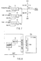
- FIG. 1 is a block diagram illustrating the structure of an information processing system according to the embodiment of the invention.
- a host system (hereinafter referred to as a "host") 10 consists of an electronic device such as a portable personal computer.
- the host 10 has a card interface 11.
- the card interface 11 has, for example, two card slots 11a and llb that enable two small card-shaped devices (hereinafter referred to simply as "cards") 20 to be inserted therein.
- FIG. 1 shows a card slot structure in which two cards 20 arranged in a single plane are inserted. Actually, however, the card slot has a structure that enables two cards 20 to be inserted in two vertical stages.
- the card interface 11 assigns, to each card 20, a clock (CLK) line, a command (CMD) line, and four signal lines (DAT[3:0] line) that can be assigned to be used, for example, as data lines.
- DAT[3:0] indicates four signal lines DAT[3] - DAT[0].
- FIG. 1 does not show a power supply (VDD) line or a ground (GND) line.
- the CLK line can be commonly used for different cards 20. Therefore, in the embodiment, CLK lines for respective cards 20 are connected on the card interface 11, thereby enabling the CLK lines to be commonly driven by the host 10. The same can be said of the VDD and GND lines.
- the host 10 includes an initialization basic driver 141 for executing a process for initializing each card 20.
- each card 20 has a card register file 21.
- the card register file 21 includes a group of registers that pre-store respective data items such as an operating voltage, a card ID, a card address, a card type and an operation mode, etc. for each card 20.
- the card ID is identification data peculiar to each card 20.
- the card address is an address pre-assigned to each card 20.
- the card type indicates whether each card 20 is a memory card or an I/O card. The operation mode will be described later. If each card 20 is an I/O card, it also includes a system I/O register 22.
- the system I/O register 22 pre-stores plug-and-play information (hereinafter referred to as "PnP information") necessary for realizing a plug-and-play function.
- the PnP information includes data indicating the type of the I/O card, data as to whether or not a device driver peculiar to the I/O card is incorporated therein, and data indicating the version of the driver, if there is one.
- a Bluetooth interface, a USB (Universal Serial Bus) interface, a LAN (Local Area Network) interface, a GPS (Global Positioning System) interface and a portable telephone interface, etc. are considered as I/O cards.
- FIG. 2 shows a rough structure of the host 10, and the structure of an I/O card 20a as the card 20.
- the host 10 has, as well as the card interface 11, a CPU (Central Processing Unit) 12, a system memory 13 and a disk storage system 14.
- the CPU 12 controls the entire host 10.
- the system memory 13 is used to store various types of data, and programs to be executed by the CPU 12.
- the system memory 13 is formed of, for example, a RAM (Random Access Memory).
- the disk storage system 14 is formed of, for example, a hard disk drive.
- the disk storage system 14 incorporates various types of device drivers 142, as well as the initialization basic driver 141.
- the device drivers 142 include device drivers prepared for and peculiar to the respective types of I/O cards.
- the I/O card 20a has a connector section 23 in which nine signal pins with the numbers 1 - 9 are arranged.
- the signal terminals provided in the connector section 23 are called “signal pins".
- this name does not necessarily indicate the shape of the signal terminals.
- the signal pins provided in the connector section 23 are printed pads.
- a pin, numbered 1, is called “DAT 3 (DAT[3])", and can be assigned to be used, for example, as a data terminal.
- a pin, numbered 2 is called “CMD”, and is assigned to be used as a terminal for transferring a command from the host 10 to the I/O card 20a, and a response to the command from the I/O card 20a to the host 10.
- a pin, numbered 3 is called “GND (Vss1)” and assigned to be used as a first ground signal terminal.
- a pin, numbered 4, is called “VDD” and assigned to be used as a power signal terminal.
- a pin, numbered 5, is called “CLK” and assigned to be used as a clock terminal.
- a pin, numbered 6, is called “GND (Vss2)” and assigned to be used as a second ground signal terminal.
- a pin, numbered 7, is called “DAT 0 (DAT[0])", and is assigned to be used as a data terminal.
- Pins, numbered 8 and 9, are called “DAT 1 (DAT[1])” and “DAT 2 (DAT[2])", respectively, and are assigned to be used as data terminals.
- the above-mentioned pin arrangement and signal assignment to each pin in the I/O card 20a are commonly employed in different types of I/O cards 20a. Further, the same can be said of memory cards. In other words, the same pin arrangement and the same signal assignment are employed in all types of cards 20.
- signals assigned to DAT[3] - DAT[0] (DAT[3:0]) differ between different types of cards 20.
- signals assigned to those pins differ between different types of I/O cards 20a.
- DAT[3] - DAT[0] are assigned to be used as respective bidirectional data lines (data terminals).
- DAT[3] is also assigned to be used as a card detection terminal. Signal assignment concerning DAT[3] - DAT[0] in the case of the I/O card 20a will be described later.
- the I/O card 20a has a processor module 200.
- the processor module 200 includes a controller 201, a ROM 202, a SRAM (Static RAM) 203, an I/O interface 204, an external interface 205 and a memory interface 206.
- the controller 201 is a microprocessor for controlling the entire I/O card 20a.
- the ROM 202 stores control programs to be executed by the controller 201.
- a predetermined area of the ROM 22 is assigned to be used as the card register file 21 shown in FIG. 1.
- the SRAM 203 is used as a work/buffer memory incorporated in the processor module 200.
- the I/O interface 204 is connected to the nine signal pins of the I/O card 20a and serves as an interface between the I/O card 20a and the host 10.
- the external interface 205 serves as an interface between the I/O card 20a and an external I/O device 60.
- the memory interface 206 serves as an interface for a flash memory (not shown).
- This flash memory is incorporated in the I/O card 20a and formed of a non-volatile programmable memory. A predetermined area of the flash memory is assigned to be used as the aforementioned system I/O register 22. However, the system I/O register 22 may be incorporated in the processor module 200. This structure is applied to an I/O card 20a that does not always need the flash memory.
- a card 20 is inserted in one of the card slots lla and llb of the card interface 11, when the host is in an ON (power-on) state.
- a power signal and a ground signal are supplied from the host 10 to the card 20 via the VDD line and the GND line, respectively.
- the card 20 reaches a power-on state.
- a clock signal is also supplied from the host 10 to the card 20 via the CLK line. The same state is also reached when the host 10 is turned on after the card 20 is inserted into one of the card slots of the card interface 11.
- the initialization basic driver 141 incorporated in the host 10 starts the card initialization process.
- the card initialization process is executed by the host 10.
- the card initialization process is also started when a reset command is output from the host 10 to the card 20 via a CMD line corresponding to the card 20 and incorporated in the card interface 11 (step S0). It is a matter of course that the initialization basic driver 141 operates after it is loaded from the disk storage system 14 to the system memory 13.
- a power supply voltage supplied from the host to the card 20 via the VDD line is set at a value predetermined irrespective of the type of the card. This voltage will be called an "initial voltage".
- the card 20 executes receipt of a command and transmission of a response in reply to the command, using only the CMD line. This operation is performed irrespective of the card type.
- the mode for executing the card initialization process is roughly divided into two modes -- a Card Identification Mode and a Data Transfer Mode.
- the Card Identification Mode the card 20 has one of three states -- an Idle State, a Ready State and an Identification State.
- the Data Transfer Mode the card 20 has one of three states -- a Standby State, a Transfer State and an Inactive State.
- step S1 When the host 10 starts the card initialization process, the operation condition of a card 20 to be subjected to the card initialization process is confirmed (step S1).
- the step S1 will be described in more detail.
- the host 10 supplies, from the card interface 11 to the card 20 to be subjected to the card initialization process, a first command for confirming the operation condition of the card 20. More specifically, the host 10 serially supplies the first command to the card 20 via the CMD line between the host 10 and the card 20 in synchronism with a clock signal on the CLK line.
- the card 20 Upon receiving the first command, the card 20 selects, from the card register file 21, an operation condition including its operating voltage. The card 20 then serially supplies the host 10 with a response, in which the operation condition is set, in reply to the first command via the CMD line in synchronism with the clock signal.
- FIG. 4 shows the relationship between the command output from the host 10 to the card 20, the response output in reply to the command from the card 20 to the host 10, and the clock signal on the CLK line.
- the host 10 receives the response output from the card 20 in reply to the first command.
- the response contains the operation condition of the card 20 including the operating voltage.
- the host 10 confirms the operating voltage included in the operation condition of the card 20.
- the host 10 After executing the step S1, the host 10 resets the power supply voltage on the VDD line from the initial voltage to the operating voltage of the card 20 (step S2). Thus, the power supply voltage on the VDD line is switched to an operating voltage suitable for the card 20 connected to the card interface 11 of the host 10. After that, the host 10 supplies, via the CMD line, the card 20 with a second command for informing the card 20 of the newly set power supply voltage (operating voltage), and confirming the operation state of the card 20 at this operating voltage (step S2a).
- the second command contains, as an argument, information indicating the newly set operating voltage.
- the card 20 receives the second command supplied from the host 10. If the card 20 is in a state in which it can be operated by the newly set power supply voltage, i.e. the operating voltage indicated by the received command, the card 20 supplies the host 10 with a response indicating its ready state, via the CMD line. On the other hand, if the card is not in that state, the card 20 supplies the host 10 with a response indicating its busy state, via the CMD line.
- step S3 Until receiving the response indicating the ready state of the card 20 (step S3), the host 10 supplies the second command to the card 20 (step S2a).
- the host 10 Upon receiving the response indicating the ready state of the card 20, the host 10 determines that the card 20 has been sifted from the Idle State to the Ready State.
- the host 10 When determining that the card 20 has reached the Ready State, the host 10 acquires a card ID from the card 20 (step S4).
- the step S4 will be described in detail.
- the host 10 supplies the card 20, via the CMD line, with a third command for acquiring the card ID from the card 20.
- the card 20 receives the third command output from the host 10.
- the card 20 acquires its own card ID from the card register file 21.
- the card 20 supplies the host 10 with a response, having its own card ID set therein, in reply to the third command via the CMD line.
- the host 10 receives the response output from the card 20 in reply to the third command. Subsequently, the host 10 extracts the card ID of the card 20 from the response. This card ID is transferred to an application program 143 (see FIG. 5) for using the card 20. As a result, the card 20 shifts from the Ready State to the Identification State. This Identification State is the final state of the Card Identification Mode.
- the above-described operations are the details of the step S4.
- the host 10 acquires a card address from the card 20 in the Identification State (step S5).
- the step S5 will be described in detail.
- the host 10 supplies the card 20, via the CMD line, with a fourth command for acquiring the card address from the card 20.
- the card 20 receives the fourth command output from the host 10.
- the card 20 acquires its own card address from the card register file 21.
- the card 20 supplies the host 10 with a response, having its own card address set therein, in reply to the fourth command via the CMD line.
- the host 10 receives the response output from the card 20 in reply to the fourth command. Subsequently, the host 10 extracts the card address of the card 20 from the response, thereby identifying the card 20. As a result, the host 10 shifts from the Card Identification Mode to the Data Transfer Mode, while the card 20 reaches the Standby State as the initial state of the Data Transfer Mode.
- the host 10 selects, using the card address acquired at the step S5, a card 20 to which the card address is assigned (step S6).
- the step S6 will be described in detail.
- the host 10 uses the acquired card address to output a fifth command for selecting the card 20 to which the card address is assigned, to each CMD line on the card interface 11. Then, that one of the cards 20 connected to the card interface 11 of the host 10 reaches a selected state, to which the card address indicated by the fifth command from the host 10 is assigned, and which is now in a non-selected state.
- the card 20 having reached the selected state supplies the host 10, via the CMD line, with a response indicating that the card itself has been selected. As a result, the card 20 shifts from the Standby State to the Transfer State.
- the host 10 determines that the card 20 designated by the fifth command has been selected, and hence the card 20 has shifted to the Transfer State.
- the host 10 reads the card type and the operation mode of the card 20 selected at the step S6 (step S7).
- the step S7 will be described in detail.
- the host 10 supplies the card 20, via the CMD line, with a sixth command for reading the card type and the operation mode of the card 20.
- the card 20 receives the sixth command.
- the card 20 acquires its own card type and operation mode from the card register file 21.
- the card 20 supplies the host 10 with a response, having its own card type and operation mode set therein, in reply to the sixth command via the CMD line.
- the host 10 receives the response output from the card 20 in reply to the sixth command.
- the host 10 extracts, from the response, the card type and operation mode of the card 20 selected at the step S6.
- the above-described operations are the details of the step S7.
- the operation mode of the card 20 differs between a case where the card 20 is a memory card and a case where it is an I/O card.
- the operation mode is only one, i.e. a 4-bit transfer mode.
- the I/O card has five operation modes, i.e. (1) a 4-bit transfer mode, (2) a 1-bit I/O transfer mode, (3) a 2-bit I/O transfer mode, (4) a USB I/O transfer mode, and (5) a 1394 I/O transfer mode.
- Each transfer (operation) mode for the I/O card is collectively called an "I/O interface mode".
- the transfer (operation) mode (4-bit transfer mode) for the memory card is called a "memory interface mode".
- the host 10 When the host 10 has acquired information indicating the card type and the operation mode of the selected card 20, it determines form the card type whether the card 20 is an I/O card or a memory card (step S8). In accordance with the determination result and the acquired operation mode, the host 10 executes a step S9a or S9b. At the step S9a or S9b, signal assignment to the card interface 11 is executed. This signal assignment corresponds to signal assignment to each signal pin of the card 20 (20a). Further, at the step S9a or S9b, a seventh command is supplied to the selected card 20 via a corresponding CMD line. The seventh command is used for informing the card 20 that its mode can be changed from the mode set at the start of the initialization process, in which only the CMD line is used, to an operation (transfer) mode peculiar to the card 20.
- the card 20 Upon receiving the seventh command output from the host 10, the card 20 sets its mode at the operation mode peculiar thereto. As a result, the card 20 can operate in a state in which signal assignment determined by the peculiar operation mode has been executed on each of the signal pins DAT[3] - DAT[0].
- the host 10 can use, when initializing a card 20, a mode peculiar to the card 20 as the operation mode including signal assignment to each of the signal pins (data terminals) DAT[3] - DAT[0] of the card 20, irrespective of, for example, the type of the card 20.
- the host 10 can set the operation mode of an I/O card having the same pin arrangement as a memory card, using the same procedure as that for the memory card, irrespective of the type of the I/O card.
- the 4-bit transfer mode is effective in the case of an I/O card for a high-speed communication interface, which transfers a large amount of data at one time although it does not execute data transfer (i.e. transaction) many times.
- an interrupt line cannot be assigned, contrast to the case of a 1-bit or 2-bit I/O transfer mode described later. Accordingly, the termination of transfer must be determined by, for example, polling.
- the pin DAT[0] is assigned to be used as a bidirectional data line.
- the pin DAT[1] is assigned to be used as a general purpose signal line from the I/O card (20a) to the host 10.
- the pin DAT[2] is assigned to be used as a WAIT/READY line for informing the host 10 of the state (WAIT/READY) of the I/O card (20a) in synchronism with a clock signal.
- the pin DAT[3] is assigned to be used as an interrupt line (INT/WAKE line) for outputting an asynchronous interrupt signal from the I/O card (20a) to the host 10.
- the asynchronous interrupt signal sent via the INT/WAKE line is one of two types of signals.
- One is an interrupt signal (INT signal) output from the I/O card (20a) for informing the host 10 of, for example, the termination of data transfer.
- the other is an interrupt signal (WAKE signal) output from the I/O card (20a) for waking up the host 10 when the host is in a power down state or a suspended state, thereby restoring the host 10 to a normal operation state.
- This WAKE signal is output when the host 10 is in the power down state or the suspended state, therefore only the required minimum function of the I/O card (20a) is operable, and this function has detected a predetermined interface state.
- the predetermined interface state indicates, for example, that state of an I/O card having a telephone communication function, such as a modem interface, in which the card has received a call signal.
- the general purpose signal line DAT[1]
- DAT[1] can be used as an audio line.
- the 1-bit transfer mode is effective in the case of an I/O card as an interface, which requires prompt start of data transfer (transaction) since it executes data transfer many times, although it does not transfer a large amount of data at one time.
- the pins DAT[1] and DAT[0] are assigned to be used as bidirectional data lines.
- the pin DAT[2] is assigned to be used as a WAIT/READY line as in the 1-bit I/O transfer mode.
- the pin DAT[3] is assigned to be used as an INT/WAKE line as in the 1-bit I/O transfer mode.
- the 2-bit I/O transfer mode differs from the 1-bit I/O transfer mode in that the pin DAT[1] is assigned to be used as a data line and not as a general purpose signal line.
- the 2-bit I/O transfer mode is effective in the case of an I/O card as a LAN interface, which does not require a general purpose signal line but requires higher-speed transfer (higher-speed communication) than the I/O card that uses the 1-bit I/O transfer mode.
- the USB I/O transfer mode is effective where the I/O card (20a) is a USB interface.
- the pins DAT[1] and DAT[0] are assigned to be used as USB data lines.
- the 1394 I/O transfer mode is effective where the I/O card (20a) is an IEEE (Institute of Electrical and Electronics Engineers, Inc.) 1394 interface.
- the four signal lines DAT[3] - DAT[0], i.e. DAT[3:0] are assigned to be used as IEEE 1394 data lines.
- the cells 71, 72 and 73 have host-side 1-bit input/output terminals 71a, 72a and 73a and card-side 1-bit input/output terminals 71b, 72b and 73b, respectively.
- the 1-bit input/output terminals 71b, 72b and 73b are connected to each signal line DAT[i] of the card interface 11.
- the I/O cell 71 is used for realizing an interface function peculiar to the operation mode of the card 20, if the operation mode is a transfer mode, i.e.
- the I/O cell 72 or 73 is each used for realizing an interface function peculiar to the operation mode of the card 20, if the operation mode is the USB I/O transfer mode or the 1394 I/O transfer mode.
- the interface function of each cell 71, 72 or 73 can be turned on or off from the outside.
- the signal line DAT[i] is connected to an end of an active pull-up resister 74 and an end of an active pull-down resister 75.
- the resisters 74 and 75 can be turned on and off from the outside.
- the initialization basic driver 141 in the host 10 turns on only that one of the cells 71, 72 and 73, which corresponds to the operation mode of a card 20 selected at the step S6, in order to enable the realization of an interface function peculiar to the operation mode. Further, the initialization basic driver 141 turns on and off the resisters 74 and 75 in accordance with the operation mode.
- the host 10 After the host 10 acquires information indicating the card type and the operation mode of the card 20 selected at the step S6 (step S7), it determines from the card type whether the card 20 is a memory card or an I/O card (step S8).
- the host 10 executes signal assignment on the card interface 11 on the basis of the operation mode peculiar to the memory card and obtained at the step S7 (step S9b). Further, at the step S9b, the host 10 supplies the card 20, via the CMD line, with the seventh command for informing the card 20 that the mode can be changed to the operation mode peculiar to the card 20. After executing the step S9b, the host 10 determines that the initialization process on the card 20 (memory card) has finished. In this state, the host 10 can be operated using the card 20 (memory card) (step S16).
- the host 10 executes signal assignment on the card interface 11 on the basis of the operation mode obtained at the step S7, as in the case of the memory card (step S9a). Further, at the step S9a, the host 10 supplies the card 20 with the seventh command.
- the host 10 determines that the initialization process on the I/O card is not completed simply by executing the step S9a. This is because when the card 20 is an I/O card, configuration settings for realizing a plug-and-play function are necessary.
- the host 10 reads the contents (PnP information) of the system I/O register 22 from the previously selected card 20, i.e. the I/O card 20a (step S10).
- the step S10 will be described in detail.
- the host 10 supplies the card 20a, via the CMD line, with an eighth command for reading the PnP information from the system I/O register 22 in the I/O card 20a.
- the card 20a receives the eighth command output from the host 10.
- the card 20a reads the PnP information from the system I/O register 22.
- the card 20a supplies the host 10 with a response, having the read PnP information set therein, in reply to the eighth command via the CMD line.
- the host 10 receives the response output from the card 20a in reply of the eighth command, and reads, from the response, the PnP information peculiar to the I/O card 20a.
- the above operations are the details of the step S10.
- the host 10 After reading the PnP information peculiar to the I/O card 20a, the host 10 refers to it (step S11). From the PnP information, the host 10 determines whether or not a device driver 142a (see FIG. 5) is attached to the I/O card 20a (step S12). The device driver 142a is peculiar to the I/O card 20a connected to the card interface 11 of the host 10. Attaching the device driver 142a to the I/O card 20a means that the driver 142a is stored in the ROM 202 incorporated in the I/O card 20a.
- the initialization basic driver 141 in the host 10 determines whether or not the device driver 142a attached to the I/O card 20a has already been downloaded as a device driver 142b (see FIG. 5) into the host 10 (step S13a). If the device driver 142a is already downloaded as the device driver 142b, the initialization basic driver 141 determines whether or not the version of the driver 142b is older than the version indicated by the PnP information (step S13b).
- step S14 is executed even when the device driver 142b has been downloaded, if the version of the device driver 142b is older than that indicated by the PnP information.
- the device driver 142a stored in the ROM 202 of the I/O card 20a is downloaded as the device driver 142b into the host 10 via a data line determined by the operation (transfer) mode of the card 20a, as is shown in FIG. 5.
- the next step et seq. are executed under the control of the device driver 142b, in place of the initialization basic driver 141.
- the next step i.e.
- a system configuration for the I/O card 20a is automatically set up in the host 10 by the downloaded updated device driver 142b on the basis of the PnP information.
- the plug-and-play function can be realized for each card 20 (20a) connected to the host 10, even when different device drivers corresponding to the respective types of cards 20 are not pre-installed in the host 10.
- step S12 if no device driver 142a is attached to the I/O card 20a (step S12), the steps S13a, S13b and S14 are skipped over, and the step S15 is executed.
- step S15 the system configuration for the I/O card 20a is automatically set up on the basis of the PnP information by that one of the device drivers 142 installed in the host 10, which is peculiar to the type of the I/O card 20a.
- step S14 is skipped over and the step S15 is executed.
- step S15 automatic configuration settings for the I/O card 20a are executed on the basis of the PnP information by the device driver 142b that is already downloaded to the host 10.
- the host 10 After the automatic configuration settings for the I/O card 20a finish, the host 10 reaches a state in which it is operable using the I/O card 20a (20) (step S16).
- an application program 143 incorporated in the host 10 can use the card 20 (20a) and execute thereon a process peculiar thereto.
- the system shown in FIG. 2 requires, between the system memory 13 of the host 10 and the card 20a, a data transfer unit for executing data transfer.
- this type of data transfer unit is provided in the card 20a.
- the data transfer unit must access the system memory 13 via the card interface 11 under the limitation of a data width (a data transfer width) usable for data transfer and employed in the card interface 11. Therefore, it is difficult to execute high-speed data transfer between the data transfer unit and the system memory 13.
- the data transfer unit is provided in the host 10.
- the data transfer unit provided in the host 10 is called a "master".
- FIG. 8 illustrates an example of a structure in which a master is provided in the host 10.
- a master 15 is interposed between the system memory 13 and the card interface 11.
- the I/O card 20a is inserted in a card slot of the card interface 11.
- the master 15 executes data transfer between the system memory 13 and the I/O card 20a.
- the master 15 can access the system memory 13 without being limited by the number of signal lines usable for data transfer and provided in the card interface 11.
- the data width of a bus that connects the system memory 13 to the master 15 is sufficiently larger than the data transfer width of the card interface 11. Accordingly, the master 15 provided in the host 10 can realize high-speed data transfer between itself and the system memory 13, without being limited by a data transfer width, even if small, between the host 10 and the card 20a.
- step S6 There is a case where the user of the host 10 wants to switch the card 20 (20a) selected at the step S6 to another card 20 (20a).
- a request for switching the card is supplied from the application program 143 shown in FIG. 5 to the initialization basic driver 141.
- the initialization basic driver 141 Upon receiving the request, the initialization basic driver 141 causes the currently selected card 20 (20a) to reach a non-selected state (step S17).
- step S17 will now be described in detail.
- the initialization basic driver 141 supplies the card 20 (20a), via the CMD line, with a ninth command for causing the currently selected card 20 (20a) to reach a non-selected state.
- the card 20 (20a) shifts to the non-selected state in accordance with the command.
- the fifth command for selecting a non-selected card 20 (20a) is the same command (a card selecting command) as the ninth command for causing a selected card 20 (20a) to reach a non-selected state.
- the card selecting command is supplied to a non-selected card 20 (20a)
- it functions as a command for selecting the card 20 (20a).
- the command is supplied to a selected card 20 (20a)
- it functions as a command for causing the selected card 20 (20a) to reach the non-selected state.
- the program After the initialization basic driver 141 causes the card 20 (20a) selected at the step S6 to reach a non-selected state at the step S17, the program returns to the step S6. At this time, the initialization basic driver 141 can select another card 20 (20a) requested by the application program 143.
- an inactivation command is supplied to the card 20 (20a) via the CMD line by the initialization basic driver 141 of the host 10 (step S18).
- the card 20 (20a) shifts from the Transfer State to the Inactive State. In this state, the supply of power to the card 20 (20a) is interrupted.
Abstract
Description
Claims (18)
- An electronic device (10) in which a card-shaped device (20, 20a) having a connector section (23) is usable, the connector section (23) being provided with connector pins including data pins, characterized by comprising:a card interface (11) to be connected to the card-shaped device (20, 20a) via the connector section (23) of the card-shaped device (20, 20a);operation mode acquiring means (141) for acquiring, when the card interface (11) is connected to the card-shaped device (20a, 20a), operation mode information of the card-shaped device (20, 20a) via a predetermined one of the connector pins of the card-shaped device (20, 20a) other than the data pins; andoperation mode setting means (41) for executing signal assignment on each of the data pins on the basis of the operation mode information acquired by the operation mode acquiring means (141).
- The electronic device (10) according to claim 1, characterized in that:the predetermined connector pin is a command pin for transferring a command from the electronic device (10) to the card-shaped device (20, 20a), and also transferring a response in reply to the command from the card-shaped device (20, 20a) to the electronic device (10); andthe operation mode acquiring means (141) acquires the operation mode information of the card-shaped device (20, 20a) by executing transfer of the command and receipt of the response via the command pin of the card-shaped device (20, 20a).
- The electronic device (10) according to claim 1, characterized by further comprising:operation condition acquiring means (141) for acquiring, via the predetermined connector pin, an operation condition of the card-shaped device (20, 20a), the operation condition including an operating voltage applied to the card-shaped device (20, 20a); andswitch means (141) for switching a power supply voltage, supplied to the card-shaped device (20, 20a), from a predetermined initial voltage to the operating voltage included in the operation condition and acquired by the operation condition acquiring means (141).
- The electronic device (10) according to claim 3, characterized in that:the predetermined connector pin is a command pin for transferring a command from the electronic device (10) to the card-shaped device (20, 20a), and also transferring a response in reply to the command from the card-shaped device (20, 20a) to the electronic device (10);the operation mode acquiring means (141) acquires the operation mode information of the card-shaped device (20, 20a) by executing transfer of the command and receipt of the response via the command pin of the card-shaped device (20, 20a); andthe operation condition acquiring means (141) acquires the operation condition of the card-shaped device (20, 20a) by executing transfer of the command and receipt of the response via the command pin of the card-shaped device (20, 20a).
- The electronic device (10) according to claim 1, characterized in that:the operation mode information of the card-shaped device (20, 20a) indicates one of first, second and third operation modes; andthe operation mode setting means (141) assigns all the data pins to a data transfer process when the operation mode information acquired by the operation mode acquiring means indicates the first operation mode; the operation mode setting means assigns a predetermined number of ones of the data pins to the data transfer process, assigns one of the remaining data pins to a process of transmitting a general purpose signal, assigns another of the remaining data pins to a process of informing the electronic device (10) of a state of the card-shaped device (20, 20a), and assigns yet another of the remaining data pins to a process of transmitting an asynchronous interrupt signal from the card-shaped device (20, 20a) to the electronic device (10), when the operation mode information indicates the second operation mode; and the operation mode setting means assigns another predetermined number, larger than the first-mentioned predetermined number, of ones of the data pins to the data transfer process, assigns one of the remaining data pins to the process of informing the electronic device of the state of the card-shaped device (20, 20a), and assigns another of the remaining data pins to the process of transmitting an asynchronous interrupt signal from the card-shaped device (20, 20a) to the electronic device (10), when the operation mode information indicates the third operation mode.
- The electronic device (10) according to claim 1,
characterized in that the operation mode acquiring means acquires, as well as the operation mode information, card type information that indicates whether the card-shaped device (20) is a memory card or an input/output card (20a), and
that the electronic device (10) further comprises:plug-and-play information acquiring means (141) for acquiring, when the card type information acquired by the operation mode acquiring means indicates that the card-shaped device (20) is the input/output card (20a), plug-and-play information necessary for realizing a plug-and-play function, from the input/output card (20a); andautomatic configuration means (141) for causing a device driver (142) peculiar to the type of the input/output card (20a) to automatically set up a system configuration for the input/output card (20a) on the basis of the plug-and-play information acquired by the plug-and-play information acquiring means (141). - The electronic device (10) according to claim 6,
characterized by further comprising downloading means (141) for downloading, from the input/output card (20a), a device driver (142, 142a) peculiar to the input/output card (20a), if the plug-and-play information acquired by the plug-and-play information acquiring means (141) from the input/output card (20a) indicates that the device driver (142, 142a) peculiar to the input/output card (20a) is attached to the input/output card (20a),
and wherein the automatic configuration means (141) causes the device driver (142, 142b) downloaded by the downloading means (141) to automatically set up the system configuration for the input/output card (20a). - The electronic device (10) according to claim 6,
characterized by further comprising means (141) for downloading a first device driver (142, 142a), peculiar to the input/output card (20a), from the input/output card (20a) to the electronic device (10), if the plug-and-play information indicates that the first device driver (142, 142a) is attached to the input/output card (20a), and if there is no second device driver (142, 142a) already downloaded to the electronic device, or there is a second device driver (142, 142b) already downloaded to the electronic device (10) but having a version older than the first device driver (142, 142a),
and wherein the automatic configuration means (141) causes an updated device driver (142, 142b) downloaded to the electronic device (10) to automatically set up the system configuration for the input/output card (20a). - The electronic device (10) according to claim 1, characterized by further comprising:a system memory (13) for storing various types of data; anda data transfer unit (15) for accessing the system memory (13) to thereby execute data transfer between the system memory (13) and the card-shaped device (20a).
- A card-shaped device (20, 20a) to be used by an electronic device (10) having a card interface (11), characterized by comprising:a connector section (23) having connector pins that include data pins, the connector section being connected to the electronic device (10) via the card interface (11);a register file (21) pre-storing operation mode information of the card-shaped device (20, 20a);transmitter means for transmitting the operation mode information, stored in the register file (21), via a predetermined one of the connector pins other than the data pins, when a command that requests reading of the operation mode information has been supplied from the electronic device (10) via the predetermined pin; anddata transfer means (201) for executing data transfer between the card-shaped device (20, 20a) and the electronic device (10), using the data pins on which signal assignment has been executed by the electronic device (10) in accordance with the operation mode information.
- The card-shaped device (20, 20a) according to claim 10, characterized in that:the predetermined pin is a command pin used for transferring a command from the electronic device (10) to the card-shaped device (20, 20a), and also transferring a response from the chard-shaped device (20, 20a) to the electronic device (10) in reply to the command; andthe transmitter means (201) transmits the operation mode information to the electronic device (10) by including the operation mode information in the response.
- The card-shaped device (20, 20a) according to claim 10, characterized in that:the register file (21) pre-stores an operation condition of the card-shaped device (20, 20a), which includes an operating voltage applied to the card-shaped device (20, 20a); andthe transmitter means (201) transmits the operation condition, stored in the register file (21), to the electronic device via the predetermined pin, when a command for confirming the operation condition has been supplied from the electronic device (10) via the predetermined pin.
- The card-shaped device (20, 20a) according to claim 10, characterized in that:the operation mode information of the card-shaped device (20, 20a) indicates one of first, second and third operation modes; andthe data transfer means (201) operates as described below when a command, which indicates that an operation mode of the card-shaped device (20, 20a) can be changed to an operation mode indicated by the operation mode information, has been supplied from the electronic device (10) via the predetermined pin as a result of signal assignment executed on the data pins by the electronic device (10) in accordance with the operation mode information; the data transfer means (201) uses all the data pins for data transfer when the operation mode information indicates the first mode; the data transfer means (201) uses a predetermined number of ones of the data pins for data transfer, uses one of the remaining data pins for transmitting a general purpose signal, uses another of the remaining data pins for informing the electronic device (10) of a state of the card-shaped device (20, 20a), and uses yet another of the remaining data pins for transmitting an asynchronous interrupt signal from the card-shaped device (20, 20a) to the electronic device (10), when the operation mode information indicates the second operation mode; and the data transfer means (201) uses another predetermined number, larger than the first-mentioned predetermined number, of ones of the data pins for data transfer, uses one of the remaining data pins for informing the electronic device (10) of the state of the card-shaped device (20, 20a), and uses another of the remaining data pins for transmitting an asynchronous interrupt signal from the card-shaped device (20, 20a) to the electronic device (10), when the operation mode information indicates the third operation mode.
- The card-shaped device (20, 20a) according to claim 10,
characterized by further comprising a system input/output register (22) pre-storing plug-and-play information necessary for realizing a plug-and-play function,
and wherein the transmitter means (201) transmits the plug-and-play information, stored in the system input/output register (22), to the electronic device (20, 20a) via the predetermined pin, when a command that requests reading of the plug-and-play information has been supplied from the electronic device (10) via the predetermined pin. - A method of setting, using an electronic device (10), an operation mode for a card-shaped device (20, 20a) connected to the electronic device (10) via a card interface (11) incorporated therein, the card-shaped device (20, 20a) being provided with a connector section (23) having connector pins that include data pins, the method characterized by comprising the steps of:acquiring operation mode information of the card-shaped device (20, 20a) via a predetermined one of the connector pins of the card-shaped device (20, 20a) other than the data pins when initializing the card-shaped device (20, 20a); andexecuting signal assignment on the data pins of the card-shaped device (20, 20a) in accordance with the operation mode information acquired at the acquiring step.
- The method according to claim 15, characterized in that the signal assignment step includes the step of informing the card-shaped device (20, 20a), via the predetermined pin after the signal assignment, that an operation mode of the card-shaped device (20, 20a) can be changed to an operation mode indicated by the operation mode information and peculiar to the card-shaped device (20, 20a).
- The method according to claim 15, characterized by further comprising the steps of:acquiring, via the predetermined pin, an operation condition of the card-shaped device (20, 20a), which includes an operating voltage applied to the card-shaped device (20, 20a), when acquiring the operation mode information of the card-shaped device (20, 20a); andswitching a power supply voltage applied to the card-shaped device (20, 20a) from a predetermined initial voltage to the operating voltage included in the acquired operation condition.
- The method according to claim 15, characterized in that:the operation mode information indicates one of first, second and third operation modes; andin the signal assignment step, all the data pins are assigned to a data transfer process when the operation mode information indicates the first operation mode; a predetermined number of ones of the data pins are assigned to the data transfer process, one of the remaining data pins is assigned to a process of transmitting a general purpose signal, another of the remaining data pins is assigned to a process of informing the electronic device (10) of a state of the card-shaped device (20, 20a), and yet another of the remaining data pins is assigned to a process of transmitting an asynchronous interrupt signal from the card-shaped device (20, 20a) to the electronic device (10), when the operation mode information indicates the second operation mode; and another predetermined number, larger than the first-mentioned predetermined number, of ones of the data pins are assigned to the data transfer process, one of the remaining data pins is assigned to the process of informing the electronic device (10) of the state of the card-shaped device (20, 20a), and another of the remaining data pins is assigned to the process of transmitting an asynchronous interrupt signal from the card-shaped device (20, 20a) to the electronic device (10), when the operation mode information indicates the third operation mode.
Applications Claiming Priority (2)
| Application Number | Priority Date | Filing Date | Title |
|---|---|---|---|
| JP2000063884 | 2000-03-08 | ||
| JP2000063884A JP4649009B2 (en) | 2000-03-08 | 2000-03-08 | Information processing apparatus having a card interface, card-type electronic equipment that can be mounted on the apparatus, and operation mode setting method in the apparatus |
Publications (3)
| Publication Number | Publication Date |
|---|---|
| EP1132824A2 true EP1132824A2 (en) | 2001-09-12 |
| EP1132824A3 EP1132824A3 (en) | 2005-11-09 |
| EP1132824B1 EP1132824B1 (en) | 2009-05-06 |
Family
ID=18583676
Family Applications (1)
| Application Number | Title | Priority Date | Filing Date |
|---|---|---|---|
| EP01104748A Expired - Lifetime EP1132824B1 (en) | 2000-03-08 | 2001-02-26 | Electronic device with card interface |
Country Status (4)
| Country | Link |
|---|---|
| US (12) | US6842818B2 (en) |
| EP (1) | EP1132824B1 (en) |
| JP (1) | JP4649009B2 (en) |
| DE (1) | DE60138584D1 (en) |
Cited By (13)
| Publication number | Priority date | Publication date | Assignee | Title |
|---|---|---|---|---|
| WO2004051491A1 (en) * | 2002-11-29 | 2004-06-17 | Nokia Corporation | A method and a system for detecting bus width, an electronic device, and a peripheral device |
| US6883718B1 (en) | 2004-02-27 | 2005-04-26 | Imation Corp. | Credit card sized memory card with host connector |
| US6890188B1 (en) | 2004-02-27 | 2005-05-10 | Imation Corp. | Memory card compatible with device connector and host connector standards |
| US6908038B1 (en) | 2004-02-27 | 2005-06-21 | Imotion Corp. | Multi-connector memory card with retractable sheath to protect the connectors |
| EP1631072A1 (en) * | 2003-05-22 | 2006-03-01 | Matsushita Electric Industrial Co., Ltd. | Function module card, host device, and control method thereof |
| WO2006051629A1 (en) * | 2004-11-12 | 2006-05-18 | Kabushiki Kaisha Toshiba | Memory card having memory element and card controller thereof |
| EP1692586A2 (en) * | 2003-12-11 | 2006-08-23 | Nokia Corporation | High speed modes for multimedia-card interface |
| US7151673B2 (en) | 2004-02-27 | 2006-12-19 | Imation Corp. | Memory card host connector with retractable shieldless tab |
| US7184264B2 (en) | 2004-09-23 | 2007-02-27 | Imation Corp. | Connectable memory devices to provide expandable memory |
| US7739487B2 (en) | 2006-01-17 | 2010-06-15 | Nokia Corporation | Method for booting a host device from an MMC/SD device, a host device bootable from an MMC/SD device and an MMC/SD device method a host device may booted from |
| US8234421B2 (en) * | 2004-04-21 | 2012-07-31 | Stmicroelectronics, Inc. | Smart card with selectively allocatable data buffers and associated methods |
| CN101655775B (en) * | 2004-12-27 | 2012-11-07 | 株式会社东芝 | Card and host apparatus |
| EP2799950A3 (en) * | 2013-04-30 | 2016-11-09 | Samsung Electronics Co., Ltd | Portable electronic device, flip-type cover of the portable electronic device, and method for controlling the flip-type cover |
Families Citing this family (63)
| Publication number | Priority date | Publication date | Assignee | Title |
|---|---|---|---|---|
| KR100566463B1 (en) | 1995-01-31 | 2006-03-31 | 가부시끼가이샤 히다치 세이사꾸쇼 | Semiconductor memory device |
| JP4649009B2 (en) | 2000-03-08 | 2011-03-09 | 株式会社東芝 | Information processing apparatus having a card interface, card-type electronic equipment that can be mounted on the apparatus, and operation mode setting method in the apparatus |
| US6438638B1 (en) * | 2000-07-06 | 2002-08-20 | Onspec Electronic, Inc. | Flashtoaster for reading several types of flash-memory cards with or without a PC |
| US7295443B2 (en) | 2000-07-06 | 2007-11-13 | Onspec Electronic, Inc. | Smartconnect universal flash media card adapters |
| US6820148B1 (en) * | 2000-08-17 | 2004-11-16 | Sandisk Corporation | Multiple removable non-volatile memory cards serially communicating with a host |
| US7107378B1 (en) | 2000-09-01 | 2006-09-12 | Sandisk Corporation | Cooperative interconnection and operation of a non-volatile memory card and an input-output card |
| CN100493096C (en) * | 2001-07-25 | 2009-05-27 | 索尼公司 | Interface apparatus |
| JP4082913B2 (en) * | 2002-02-07 | 2008-04-30 | 株式会社ルネサステクノロジ | Memory system |
| US7440774B2 (en) | 2002-04-08 | 2008-10-21 | Socket Mobile, Inc. | Wireless enabled memory module |
| DE10230619A1 (en) * | 2002-07-03 | 2004-01-29 | Siemens Ag | radio module |
| US7526791B2 (en) * | 2002-07-24 | 2009-04-28 | Broadcom Corporation | System and method for an interactive broadband system-on-chip with a reconfigurable interface |
| KR100440972B1 (en) * | 2002-07-27 | 2004-07-21 | 삼성전자주식회사 | Apparatus and method for establishing data transfer mode by card insertion identification |
| US20040054836A1 (en) * | 2002-09-18 | 2004-03-18 | Cheng-Shing Lai | Method of data access by simulating an external device to be a hard disk drive |
| US7367503B2 (en) * | 2002-11-13 | 2008-05-06 | Sandisk Corporation | Universal non-volatile memory card used with various different standard cards containing a memory controller |
| US20050055479A1 (en) * | 2002-11-21 | 2005-03-10 | Aviad Zer | Multi-module circuit card with inter-module direct memory access |
| US8037229B2 (en) * | 2002-11-21 | 2011-10-11 | Sandisk Technologies Inc. | Combination non-volatile memory and input-output card with direct memory access |
| US20040203976A1 (en) * | 2002-12-30 | 2004-10-14 | Gupta Vivek G. | Power management for nodes coupled to a communication link |
| US7365454B2 (en) * | 2003-02-11 | 2008-04-29 | O2Micro International Limited | Enhanced power switch device enabling modular USB PC cards |
| US8463951B1 (en) * | 2003-03-27 | 2013-06-11 | Nvidia Corporation | Unified driver architecture device identifier strategy |
| EP1473630A3 (en) * | 2003-04-11 | 2007-10-10 | Samsung Electronics Co., Ltd. | Computer system and method of setting an interface card therein |
| US7305535B2 (en) * | 2003-04-17 | 2007-12-04 | Sandisk Corporation | Memory cards including a standard security function |
| US20040249992A1 (en) * | 2003-04-30 | 2004-12-09 | Komarla Eshwari P. | Methods and apparatus to provide environment-based instruction selection |
| FI20035072A0 (en) * | 2003-05-22 | 2003-05-22 | Nokia Corp | Interface bus, electronic device and system |
| US6973519B1 (en) * | 2003-06-03 | 2005-12-06 | Lexar Media, Inc. | Card identification compatibility |
| KR100475125B1 (en) | 2003-06-21 | 2005-03-14 | 삼성전자주식회사 | Movable storage apparatus capable of freely changing width of data bus and method for setting width of data bus of the same |
| DE10339436A1 (en) * | 2003-08-24 | 2005-04-07 | Nova Informationstechnik Gmbh | Method and device for constructing a virtual electronic teaching system with individual interactive communication |
| US7209995B2 (en) | 2003-12-09 | 2007-04-24 | Sandisk Corporation | Efficient connection between modules of removable electronic circuit cards |
| KR101083366B1 (en) * | 2003-12-11 | 2011-11-15 | 삼성전자주식회사 | Memory system and method for setting data transfer speed between host and memory card |
| US7844767B2 (en) * | 2004-05-21 | 2010-11-30 | Intel Corporation | Method for identifying bad lanes and exchanging width capabilities of two CSI agents connected across a link |
| US7325167B2 (en) * | 2004-09-24 | 2008-01-29 | Silicon Laboratories Inc. | System and method for using network interface card reset pin as indication of lock loss of a phase locked loop and brownout condition |
| US7464193B2 (en) * | 2005-08-29 | 2008-12-09 | Sandisk Il Ltd. | Device and method for configuring a flash memory controller |
| JP2007156512A (en) * | 2005-11-30 | 2007-06-21 | Brother Ind Ltd | Status information acquisition processing program, status information acquisition device, and status information acquisition system |
| JP4829621B2 (en) * | 2006-01-24 | 2011-12-07 | マルホン工業株式会社 | Gaming machine management system and gaming machine used in the gaming machine management system |
| KR101223986B1 (en) * | 2006-02-23 | 2013-01-18 | 삼성전자주식회사 | Smart card and smart card system supporting plurality of interfaces |
| JP4724573B2 (en) * | 2006-03-02 | 2011-07-13 | 株式会社リコー | Transfer system switching circuit in interface circuit |
| US20070257116A1 (en) * | 2006-05-04 | 2007-11-08 | Hsiang-An Hsieh | Interface detection method of a multiple mode micro memory card |
| JP5011818B2 (en) * | 2006-05-19 | 2012-08-29 | 富士通セミコンダクター株式会社 | Semiconductor memory device and test method thereof |
| US8719709B2 (en) * | 2006-08-25 | 2014-05-06 | Sandisk Technologies Inc. | Method for interfacing with a memory card to access a program instruction |
| JP2008059466A (en) * | 2006-09-01 | 2008-03-13 | Toshiba Corp | Electronic apparatus and control method for it |
| US8013332B2 (en) * | 2006-10-20 | 2011-09-06 | Sandisk Technologies Inc. | Portable memory devices |
| US7928010B2 (en) * | 2006-10-20 | 2011-04-19 | Sandisk Corporation | Method for producing portable memory devices |
| TWI407860B (en) * | 2006-10-20 | 2013-09-01 | Sandisk Technologies Inc | Portable memory devices and method therefor |
| JP2009054103A (en) * | 2007-08-29 | 2009-03-12 | Panasonic Corp | Host apparatus for controlling multiple memory cards |
| JP2009086988A (en) * | 2007-09-28 | 2009-04-23 | Toshiba Corp | Memory card |
| CN101910972B (en) * | 2008-02-29 | 2013-03-20 | 松下电器产业株式会社 | Interface device for host device, interface device for slave device, host device, slave device, communication system and interface voltage switching method |
| JP5106219B2 (en) | 2008-03-19 | 2012-12-26 | 株式会社東芝 | Memory device, host device, memory system, memory device control method, host device control method, and memory system control method |
| US20090327634A1 (en) * | 2008-06-25 | 2009-12-31 | Microsoft Corporation | Secure configuration of transient storage devices |
| JP5341503B2 (en) * | 2008-12-26 | 2013-11-13 | 株式会社東芝 | Memory device, host device, and sampling clock adjustment method |
| US8249656B2 (en) * | 2009-02-15 | 2012-08-21 | Google Inc. | Wireless communicator jacket with multiple operational stages |
| US7996596B2 (en) * | 2009-07-17 | 2011-08-09 | Dell Products, Lp | Multiple minicard interface system and method thereof |
| WO2011050740A1 (en) * | 2009-10-30 | 2011-05-05 | 北京飞天诚信科技有限公司 | Method for identifying multi-seat card reader and communication method and system with main computer thereof |
| US7865629B1 (en) * | 2009-11-24 | 2011-01-04 | Microsoft Corporation | Configurable connector for system-level communication |
| JP2012068996A (en) * | 2010-09-24 | 2012-04-05 | Toshiba Denpa Products Kk | Cpu board |
| JP5728292B2 (en) * | 2011-02-04 | 2015-06-03 | 株式会社東芝 | Memory device and host system |
| US20130250140A1 (en) * | 2012-03-26 | 2013-09-26 | Aptos Technology Inc. | Composite memory card and dedicated reader |
| US9582010B2 (en) * | 2013-03-14 | 2017-02-28 | Rackspace Us, Inc. | System and method of rack management |
| KR102284654B1 (en) * | 2014-07-02 | 2021-08-03 | 삼성전자 주식회사 | Memory card |
| US9767045B2 (en) | 2014-08-29 | 2017-09-19 | Memory Technologies Llc | Control for authenticated accesses to a memory device |
| CN105988078B (en) * | 2015-02-28 | 2020-03-24 | 智恒(厦门)微电子有限公司 | Method and system for realizing single-wire programmable circuit |
| CN104936125B (en) * | 2015-06-18 | 2017-07-21 | 三星电子(中国)研发中心 | surround sound implementation method and device |
| US11113425B2 (en) * | 2018-01-17 | 2021-09-07 | Crowd Strike, Inc. | Security component for devices on an enumerated bus |
| CN111144626A (en) * | 2019-12-10 | 2020-05-12 | 珠海格力电器股份有限公司 | DTU module management method and system |
| US20210390070A1 (en) * | 2020-06-16 | 2021-12-16 | Hewlett Packard Enterprise Development Lp | Universal industrial i/o interface bridge |
Citations (3)
| Publication number | Priority date | Publication date | Assignee | Title |
|---|---|---|---|---|
| US5696970A (en) * | 1993-04-01 | 1997-12-09 | Intel Corporation | Architecture for implementing PCMCIA card services under the windows operating system in enhanced mode |
| WO1999049415A2 (en) * | 1998-03-26 | 1999-09-30 | Gemplus | Versatile interface smart card |
| EP0981805A1 (en) * | 1997-05-15 | 2000-03-01 | Mondex International Limited | Ic card with shell feature |
Family Cites Families (43)
| Publication number | Priority date | Publication date | Assignee | Title |
|---|---|---|---|---|
| US481629A (en) * | 1892-08-30 | Potato-cutter | ||
| US5237674A (en) | 1987-04-11 | 1993-08-17 | Apple Computer, Inc. | Self identifying scheme for memory module including circuitry for identfying accessing speed |
| JPH02190955A (en) | 1989-01-20 | 1990-07-26 | Hitachi Ltd | Input/output control system |
| JP2505298B2 (en) * | 1990-03-02 | 1996-06-05 | 富士通株式会社 | Variable bus width designation method and variable bus width information reception method in split bus |
| JPH0540728A (en) * | 1991-08-07 | 1993-02-19 | Nec Corp | Bus control method |
| US5516344A (en) * | 1992-01-10 | 1996-05-14 | International Fuel Cells Corporation | Fuel cell power plant fuel processing apparatus |
| FR2689986A1 (en) * | 1992-04-08 | 1993-10-15 | Aerospatiale | Simulator including thermal batteries. |
| WO1994011802A1 (en) * | 1992-11-12 | 1994-05-26 | New Media Corporation | Reconfigureable interface between a computer and peripheral devices |
| US5440244A (en) * | 1993-02-10 | 1995-08-08 | Cirrus Logic, Inc. | Method and apparatus for controlling a mixed voltage interface in a multivoltage system |
| US6325291B1 (en) * | 1994-04-19 | 2001-12-04 | Smarrt Diskette Gmbh | Apparatus and method for transferring information between a smart diskette device and a computer |
| EP0683594B1 (en) * | 1994-04-20 | 2000-07-12 | Canon Kabushiki Kaisha | Data processing apparatus |
| US5768542A (en) * | 1994-06-08 | 1998-06-16 | Intel Corporation | Method and apparatus for automatically configuring circuit cards in a computer system |
| CA2135505C (en) * | 1994-11-09 | 1999-11-09 | Patrick K. Kam | Dma emulation for non-dma capable interface cards |
| JPH08211973A (en) | 1995-01-26 | 1996-08-20 | Mitsubishi Electric Corp | Pc card |
| JPH0916735A (en) * | 1995-06-26 | 1997-01-17 | Mitsubishi Electric Corp | Pc card |
| US6393492B1 (en) * | 1995-11-03 | 2002-05-21 | Texas Instruments Incorporated | Method and arrangement for operating a mass memory storage peripheral computer device connected to a host computer |
| JP3565967B2 (en) * | 1995-12-21 | 2004-09-15 | 富士通株式会社 | IC card reading / writing device and IC card system |
| JPH09179802A (en) * | 1995-12-27 | 1997-07-11 | Mitsubishi Electric Corp | Multi function type pc card |
| US5752048A (en) * | 1996-02-12 | 1998-05-12 | Motorola, Inc. | Device and method for providing a simulation of an idle UART to prevent computer lockup |
| US5671368A (en) * | 1996-02-22 | 1997-09-23 | O2 Micro, Inc. | PC card controller circuit to detect exchange of PC cards while in suspend mode |
| JP3493096B2 (en) * | 1996-06-07 | 2004-02-03 | 株式会社東芝 | Semiconductor integrated circuit, IC card, and IC card system |
| US5938750A (en) * | 1996-06-28 | 1999-08-17 | Intel Corporation | Method and apparatus for a memory card bus design |
| JPH1049257A (en) | 1996-08-05 | 1998-02-20 | Yokogawa Electric Corp | Information processor |
| US5877975A (en) * | 1996-08-13 | 1999-03-02 | Nexcom Technology, Inc. | Insertable/removable digital memory apparatus and methods of operation thereof |
| FR2753089B1 (en) * | 1996-09-09 | 1999-02-12 | Biostat | MULTI-COMPARTMENT POCKET ELECTRONIC PILL |
| JPH10171957A (en) * | 1996-12-04 | 1998-06-26 | Murata Mfg Co Ltd | Cis switching feature for pc card |
| JPH10171938A (en) * | 1996-12-05 | 1998-06-26 | Hitachi Maxell Ltd | Pc card |
| FI104921B (en) * | 1996-12-19 | 2000-04-28 | Nokia Mobile Phones Ltd | Extension card, card connection and electronic device |
| US5966723A (en) * | 1997-05-16 | 1999-10-12 | Intel Corporation | Serial programming mode for non-volatile memory |
| US6138180A (en) * | 1997-09-12 | 2000-10-24 | Symbol Technologies, Inc. | Adaptive computer peripheral for selecting a communications protocol by cycling through a plurality of given protocols |
| US6481629B1 (en) * | 1997-10-17 | 2002-11-19 | I-O Data Device, Inc. | PC card with variable width data bus communication capabilities |
| US6182173B1 (en) * | 1997-11-14 | 2001-01-30 | International Business Machines Corporation | Hot plug adapters using optical switches |
| US5928347A (en) * | 1997-11-18 | 1999-07-27 | Shuttle Technology Group Ltd. | Universal memory card interface apparatus |
| FI114839B (en) * | 1997-12-01 | 2004-12-31 | Nokia Corp | A method for providing power supply to an expansion card |
| US6182162B1 (en) * | 1998-03-02 | 2001-01-30 | Lexar Media, Inc. | Externally coupled compact flash memory card that configures itself one of a plurality of appropriate operating protocol modes of a host computer |
| JPH11275000A (en) * | 1998-03-26 | 1999-10-08 | Mitsubishi Electric Corp | Initial registration setting system for data communication card |
| US6168077B1 (en) * | 1998-10-21 | 2001-01-02 | Litronic, Inc. | Apparatus and method of providing a dual mode card and reader |
| US6279114B1 (en) * | 1998-11-04 | 2001-08-21 | Sandisk Corporation | Voltage negotiation in a single host multiple cards system |
| US6901457B1 (en) * | 1998-11-04 | 2005-05-31 | Sandisk Corporation | Multiple mode communications system |
| US6285667B1 (en) * | 1998-12-02 | 2001-09-04 | Telefonaktiebolaget Lm Ericsson | Page response on existing radio signaling channel |
| US6434654B1 (en) * | 1999-03-26 | 2002-08-13 | Koninklijke Philips Electronics N.V. | System bus with a variable width selectivity configurable at initialization |
| US6581157B1 (en) * | 1999-04-26 | 2003-06-17 | 3Com Corporation | System and method for detecting and updating non-volatile memory on an electronic adapter board installed in a computing system |
| JP4649009B2 (en) * | 2000-03-08 | 2011-03-09 | 株式会社東芝 | Information processing apparatus having a card interface, card-type electronic equipment that can be mounted on the apparatus, and operation mode setting method in the apparatus |
-
2000
- 2000-03-08 JP JP2000063884A patent/JP4649009B2/en not_active Expired - Lifetime
-
2001
- 2001-02-26 EP EP01104748A patent/EP1132824B1/en not_active Expired - Lifetime
- 2001-02-26 DE DE60138584T patent/DE60138584D1/en not_active Expired - Lifetime
- 2001-03-07 US US09/799,600 patent/US6842818B2/en not_active Expired - Lifetime
-
2004
- 2004-12-02 US US11/001,309 patent/US7051142B2/en not_active Expired - Lifetime
-
2006
- 2006-03-03 US US11/366,379 patent/US7162561B2/en not_active Expired - Lifetime
- 2006-11-17 US US11/600,776 patent/US7237052B2/en not_active Expired - Lifetime
- 2006-11-17 US US11/600,782 patent/US7350009B2/en not_active Expired - Lifetime
-
2007
- 2007-05-15 US US11/798,582 patent/US7779192B2/en not_active Expired - Fee Related
-
2008
- 2008-03-17 US US12/076,351 patent/US7774533B2/en not_active Expired - Fee Related
-
2010
- 2010-07-14 US US12/836,195 patent/US8015338B2/en not_active Expired - Fee Related
-
2011
- 2011-07-27 US US13/191,958 patent/US8219733B2/en not_active Expired - Lifetime
-
2012
- 2012-06-19 US US13/527,140 patent/US8516178B2/en not_active Expired - Fee Related
-
2013
- 2013-07-23 US US13/948,553 patent/US9367503B2/en not_active Expired - Lifetime
-
2016
- 2016-05-11 US US15/151,839 patent/US9965423B2/en not_active Expired - Fee Related
Patent Citations (3)
| Publication number | Priority date | Publication date | Assignee | Title |
|---|---|---|---|---|
| US5696970A (en) * | 1993-04-01 | 1997-12-09 | Intel Corporation | Architecture for implementing PCMCIA card services under the windows operating system in enhanced mode |
| EP0981805A1 (en) * | 1997-05-15 | 2000-03-01 | Mondex International Limited | Ic card with shell feature |
| WO1999049415A2 (en) * | 1998-03-26 | 1999-09-30 | Gemplus | Versatile interface smart card |
Cited By (27)
| Publication number | Priority date | Publication date | Assignee | Title |
|---|---|---|---|---|
| WO2004051491A1 (en) * | 2002-11-29 | 2004-06-17 | Nokia Corporation | A method and a system for detecting bus width, an electronic device, and a peripheral device |
| EP1631072A1 (en) * | 2003-05-22 | 2006-03-01 | Matsushita Electric Industrial Co., Ltd. | Function module card, host device, and control method thereof |
| US7610427B2 (en) | 2003-05-22 | 2009-10-27 | Panasonic Corporation | Functional module card for transferring digital broadcasting signal using a clock generated based on a synchronous signal extracted from a received data signal |
| EP1631072A4 (en) * | 2003-05-22 | 2007-12-26 | Matsushita Electric Ind Co Ltd | Function module card, host device, and control method thereof |
| EP1692586A4 (en) * | 2003-12-11 | 2007-12-05 | Nokia Corp | High speed modes for multimedia-card interface |
| EP1692586A2 (en) * | 2003-12-11 | 2006-08-23 | Nokia Corporation | High speed modes for multimedia-card interface |
| US7151673B2 (en) | 2004-02-27 | 2006-12-19 | Imation Corp. | Memory card host connector with retractable shieldless tab |
| US6908038B1 (en) | 2004-02-27 | 2005-06-21 | Imotion Corp. | Multi-connector memory card with retractable sheath to protect the connectors |
| US6890188B1 (en) | 2004-02-27 | 2005-05-10 | Imation Corp. | Memory card compatible with device connector and host connector standards |
| US6883718B1 (en) | 2004-02-27 | 2005-04-26 | Imation Corp. | Credit card sized memory card with host connector |
| US8234421B2 (en) * | 2004-04-21 | 2012-07-31 | Stmicroelectronics, Inc. | Smart card with selectively allocatable data buffers and associated methods |
| US7184264B2 (en) | 2004-09-23 | 2007-02-27 | Imation Corp. | Connectable memory devices to provide expandable memory |
| WO2006051629A1 (en) * | 2004-11-12 | 2006-05-18 | Kabushiki Kaisha Toshiba | Memory card having memory element and card controller thereof |
| US8671227B2 (en) | 2004-12-27 | 2014-03-11 | Kabushiki Kaisha Toshiba | Card and host apparatus |
| US9128635B2 (en) | 2004-12-27 | 2015-09-08 | Kabushiki Kaisha Toshiba | Card and host apparatus |
| CN101706709B (en) * | 2004-12-27 | 2012-12-05 | 株式会社东芝 | Card and host apparatus |
| US8423679B2 (en) * | 2004-12-27 | 2013-04-16 | Kabushiki Kaisha Toshiba | Card and host apparatus |
| US8533367B2 (en) | 2004-12-27 | 2013-09-10 | Kabushiki Kaisha Toshiba | Card and host apparatus |
| US11789521B2 (en) | 2004-12-27 | 2023-10-17 | Kioxia Corporation | Card and host apparatus |
| US8812745B2 (en) | 2004-12-27 | 2014-08-19 | Kabushiki Kaisha Toshiba | Card and host apparatus |
| CN101655775B (en) * | 2004-12-27 | 2012-11-07 | 株式会社东芝 | Card and host apparatus |
| US11169594B2 (en) | 2004-12-27 | 2021-11-09 | Kioxia Corporation | Card and host apparatus |
| US9857866B2 (en) | 2004-12-27 | 2018-01-02 | Toshiba Memory Corporation | Card and host apparatus |
| US10466771B2 (en) | 2004-12-27 | 2019-11-05 | Toshiba Memory Corporation | Card and host apparatus |
| US10747299B2 (en) | 2004-12-27 | 2020-08-18 | Toshiba Memory Corporation | Card and host apparatus |
| US7739487B2 (en) | 2006-01-17 | 2010-06-15 | Nokia Corporation | Method for booting a host device from an MMC/SD device, a host device bootable from an MMC/SD device and an MMC/SD device method a host device may booted from |
| EP2799950A3 (en) * | 2013-04-30 | 2016-11-09 | Samsung Electronics Co., Ltd | Portable electronic device, flip-type cover of the portable electronic device, and method for controlling the flip-type cover |
Also Published As
| Publication number | Publication date |
|---|---|
| US7051142B2 (en) | 2006-05-23 |
| US20070057046A1 (en) | 2007-03-15 |
| EP1132824B1 (en) | 2009-05-06 |
| US9965423B2 (en) | 2018-05-08 |
| US7237052B2 (en) | 2007-06-26 |
| JP4649009B2 (en) | 2011-03-09 |
| US6842818B2 (en) | 2005-01-11 |
| US20050092837A1 (en) | 2005-05-05 |
| US20110283024A1 (en) | 2011-11-17 |
| US7774533B2 (en) | 2010-08-10 |
| US20070220192A1 (en) | 2007-09-20 |
| EP1132824A3 (en) | 2005-11-09 |
| US9367503B2 (en) | 2016-06-14 |
| US20070067538A1 (en) | 2007-03-22 |
| US7350009B2 (en) | 2008-03-25 |
| US20060149880A1 (en) | 2006-07-06 |
| US20140032805A1 (en) | 2014-01-30 |
| US20160253281A1 (en) | 2016-09-01 |
| US20120260001A1 (en) | 2012-10-11 |
| US8015338B2 (en) | 2011-09-06 |
| US7162561B2 (en) | 2007-01-09 |
| US8516178B2 (en) | 2013-08-20 |
| US7779192B2 (en) | 2010-08-17 |
| US20100281200A1 (en) | 2010-11-04 |
| JP2001256174A (en) | 2001-09-21 |
| US20080235427A1 (en) | 2008-09-25 |
| US20010021956A1 (en) | 2001-09-13 |
| US8219733B2 (en) | 2012-07-10 |
| DE60138584D1 (en) | 2009-06-18 |
Similar Documents
| Publication | Publication Date | Title |
|---|---|---|
| US9965423B2 (en) | Electronic device with card interface | |
| US8037229B2 (en) | Combination non-volatile memory and input-output card with direct memory access | |
| US20050055479A1 (en) | Multi-module circuit card with inter-module direct memory access | |
| US20030056050A1 (en) | Card device | |
| US7044385B2 (en) | Apparatus and method for establishing data transfer mode through identification of card insertion | |
| JP3477306B2 (en) | Extended input / output interface | |
| US7162562B2 (en) | Portable electronic system and accessing method thereof | |
| JP4976993B2 (en) | Data processing apparatus and communication apparatus | |
| JP2006092266A (en) | Small card adapter |
Legal Events
| Date | Code | Title | Description |
|---|---|---|---|
| PUAI | Public reference made under article 153(3) epc to a published international application that has entered the european phase |
Free format text: ORIGINAL CODE: 0009012 |
|
| 17P | Request for examination filed |
Effective date: 20010226 |
|
| AK | Designated contracting states |
Kind code of ref document: A2 Designated state(s): AT BE CH CY DE DK ES FI FR GB GR IE IT LI LU MC NL PT SE TR |
|
| AX | Request for extension of the european patent |
Free format text: AL;LT;LV;MK;RO;SI |
|
| PUAL | Search report despatched |
Free format text: ORIGINAL CODE: 0009013 |
|
| AK | Designated contracting states |
Kind code of ref document: A3 Designated state(s): AT BE CH CY DE DK ES FI FR GB GR IE IT LI LU MC NL PT SE TR |
|
| AX | Request for extension of the european patent |
Extension state: AL LT LV MK RO SI |
|
| AKX | Designation fees paid |
Designated state(s): DE FR GB |
|
| GRAP | Despatch of communication of intention to grant a patent |
Free format text: ORIGINAL CODE: EPIDOSNIGR1 |
|
| GRAS | Grant fee paid |
Free format text: ORIGINAL CODE: EPIDOSNIGR3 |
|
| GRAA | (expected) grant |
Free format text: ORIGINAL CODE: 0009210 |
|
| AK | Designated contracting states |
Kind code of ref document: B1 Designated state(s): DE FR GB |
|
| REG | Reference to a national code |
Ref country code: GB Ref legal event code: FG4D |
|
| REF | Corresponds to: |
Ref document number: 60138584 Country of ref document: DE Date of ref document: 20090618 Kind code of ref document: P |
|
| PLBE | No opposition filed within time limit |
Free format text: ORIGINAL CODE: 0009261 |
|
| STAA | Information on the status of an ep patent application or granted ep patent |
Free format text: STATUS: NO OPPOSITION FILED WITHIN TIME LIMIT |
|
| 26N | No opposition filed |
Effective date: 20100209 |
|
| REG | Reference to a national code |
Ref country code: FR Ref legal event code: PLFP Year of fee payment: 16 |
|
| REG | Reference to a national code |
Ref country code: FR Ref legal event code: PLFP Year of fee payment: 17 |
|
| REG | Reference to a national code |
Ref country code: DE Ref legal event code: R082 Ref document number: 60138584 Country of ref document: DE Representative=s name: PATENTANWAELTE HENKEL, BREUER & PARTNER MBB, DE Ref country code: DE Ref legal event code: R082 Ref document number: 60138584 Country of ref document: DE Representative=s name: HENKEL & PARTNER MBB PATENTANWALTSKANZLEI, REC, DE Ref country code: DE Ref legal event code: R082 Ref document number: 60138584 Country of ref document: DE Representative=s name: PATENTANWAELTE HENKEL, BREUER & PARTNER, DE Ref country code: DE Ref legal event code: R081 Ref document number: 60138584 Country of ref document: DE Owner name: TOSHIBA MEMORY CORP., JP Free format text: FORMER OWNER: KABUSHIKI KAISHA TOSHIBA, KAWASAKI, KANAGAWA, JP Ref country code: DE Ref legal event code: R081 Ref document number: 60138584 Country of ref document: DE Owner name: TOSHIBA MEMORY CORPORATION, JP Free format text: FORMER OWNER: KABUSHIKI KAISHA TOSHIBA, KAWASAKI, KANAGAWA, JP |
|
| REG | Reference to a national code |
Ref country code: GB Ref legal event code: 732E Free format text: REGISTERED BETWEEN 20170831 AND 20170906 |
|
| REG | Reference to a national code |
Ref country code: FR Ref legal event code: TP Owner name: TOSHIBA MEMORY CORPORATION, JP Effective date: 20171205 |
|
| REG | Reference to a national code |
Ref country code: FR Ref legal event code: PLFP Year of fee payment: 18 |
|
| PGFP | Annual fee paid to national office [announced via postgrant information from national office to epo] |
Ref country code: DE Payment date: 20200211 Year of fee payment: 20 Ref country code: GB Payment date: 20200219 Year of fee payment: 20 |
|
| PGFP | Annual fee paid to national office [announced via postgrant information from national office to epo] |
Ref country code: FR Payment date: 20200113 Year of fee payment: 20 |
|
| REG | Reference to a national code |
Ref country code: DE Ref legal event code: R071 Ref document number: 60138584 Country of ref document: DE |
|
| REG | Reference to a national code |
Ref country code: GB Ref legal event code: PE20 Expiry date: 20210225 |
|
| PG25 | Lapsed in a contracting state [announced via postgrant information from national office to epo] |
Ref country code: GB Free format text: LAPSE BECAUSE OF EXPIRATION OF PROTECTION Effective date: 20210225 |