FIELD OF THE INVENTION
The present invention relates to writing duplicate entries
in separate cache locations simultaneously whereby cache
entries are mirrored, or written twice, in one write cycle
resulting in physically separate and independent copies of
the data.
DESCRIPTION OF RELATED ART
In storage systems of computing systems, the response time
of the storage system is greatly enhanced by the use of
cache memory. As is well known, a cache memory stores
frequently accessed data word units in cache memory as well
as in primary memory. Of course, the storage system must
maintain data coherence between the word unit in cache and
the same word unit in primary storage.
There are two strategies for maintaining word unit
coherence -- write-through cache and write-back cache. In
a write-through cache, the processor writes the modified
word unit to both the cache and primary memory to ensure
that both memories always have updated copies of the word
unit. This is the simplest and most commonly used method.
In write-back cache, the cache controller keeps track of
which word units in the cache have been modified by the
processor. This is done by marking the modified word units
with a dirty bit. Thereafter, when word units are
displaced from the cache, the word units with a dirty bit
are written to primary memory.
To increase the reliability of cache write-back storage,
storage systems have written word units twice, once each at
two separate cache memories. Accordingly, if one cache
memory fails, the word unit is preserved in the second
cache memory. This is referred to as mirror write.
Figure 1 shows an example of the conventional mirror write
system. There are two separate cache systems each with
their own controller. Cache system 10 contains controller
10A and cache 10B, while cache system 12 contains
controller 12A and cache 12B. The cache systems are
interconnected by bus 14.
There are two significant problems with the conventional
cache system in Figure 1. First, the mirror write
operation is very slow. Second, if the cache in a first
cache system fails, and the controller in the second cache
system fails, then data in cache may be inaccessible if the
controller in the first cache system can't get to the
alternate good copy of the data in the cache of the second
cache system.
A review of the mirror write operation in Fig. 1
illustrates how slow the operation is in the prior art. A
mirror write in Fig. 1 begins with a write request to
either cache system. Assume a mirror write request is
received at cache system 12. Controller 12A writes the
word unit into cache 12B. Controller 12A then reads the
word unit to cache system 10 over bus 14. Controller 10A
then writes the word unit to cache 10B. After the word
unit is successfully written to cache 10B, controller 10A
sends an acknowledge signal back to cache system 12. Cache
system 12 receives the acknowledge and sends it back to the
processor. Accordingly, the mirror write in the
conventional system requires in sequence a write operation,
a read operation, a second write operation, and two
successive acknowledge operations. In addition, if bus 14
is shared with other storage devices in addition to the two
cache systems, there may be a delay in communications
between cache systems 10 and 12.
Note also that the mirror write has not solved the second
problem of access to data if a controller in one cache
system and a cache in the other cache system fails. For
example, if controller 10A fails, data in cache 10B is not
available. If cache 12B goes bad in this situation, the
data is lost unless controller 12A can get to the data in
cache 10B through a second cycle using bus 14.
SUMMARY OF THE INVENTION
The present invention, in its broad form, resides in
apparatus and method for mirror writing in a cache memory
system as recited in claims 1 and 7 respectively.
A preferred embodiment of this invention, as described
hereinafter, provides a cache memory system in a computing
system where the cache memory system has a first cache
module storing data, a second cache module storing data,
and a controller writing data simultaneously to both the
first and second cache modules. A second controller can be
added to also write data simultaneously to both the first
and second cache modules. In a single write cycle each
controller requests access to both of the first and second
cache modules. Both cache modules send an acknowledgment
of the cache request back to the controllers. Each
controller in response to the acknowledgments from both of
the cache modules simultaneously sends the same data to
both cache modules. Both of the cache modules write the
same data into cache in their respective cache modules.
Advantageously, a combination of the cache memories is
split into quadrants, Q0, Q1, Q2 and Q3 with quadrants Q0
and Q1 in one cache memory and quadrants Q2 and Q3 in the
other cache memory. One controller simultaneously writes
the same data to both quadrants Q0 and Q3, and the other
controller simultaneously writes the same data to both
quadrants Q1 and Q2.
Preferably, as described hereinafter, if one controller
detects that the other controller has failed, the
controller detecting failure of the other controller sends
accesses to quadrants previously accessed by the failed
controller.
The great advantage realized herein is the simultaneous
mirror writing of the same data to two cache memories in a
single write cycle. Another advantage is the reliability
achieved with each of the controllers having access to both
cache memories.
Brief Description of Drawings
A more detailed understanding of the invention can be had
from the following description of a preferred embodiment,
given by way of example and to be understood in conjunction
with the accompanying drawing, wherein:
- Fig. 1 shows a conventional mirror write cache system
with two independent cache systems.
- Fig. 2 illustrates a mirror write cache system with
two interdependent cache systems in accordance with a
preferred embodiment of the invention.
- Fig. 3A shows a preferred embodiment of the invention
in more detail illustrating the invention and signals
used in the invention in a normal mirror write
operation.
- Fig. 3B shows the preferred embodiment of the
invention illustrated in Fig. 3A with the signals used
in a mirror write operation where one controller has
failed.
- Fig. 4 shows in detail half of the mirror write cache
system of Fig. 2.
- Fig. 5 is a signal timing diagram for signals in Fig. 4.
- Fig. 6, composed of Figs. 6A and 6B, is a state flow
diagram illustrating the operation of the controller
state machine in Fig. 4.
- Fig. 7, composed of Figs. 7A and 7B, is a state flow
diagram illustrating the operation of the cache state
machine in Fig. 4.
Detailed Description of Preferred Embodiments
A preferred embodiment of two coordinated cache systems in
accordance with the invention is shown in Fig. 2. The two
cache memories, Cache A and Cache B, are divided in half by
addressing. Accordingly, the total cache memory may be
viewed as four quadrants of cache, quadrants Q0 and Q1 are
in Cache A and quadrants Q2 and Q3 are in Cache B. In an
alternate embodiment the cache quadrants are not
necessarily the same size.
The cache storage system has two controllers. Controller
20, writes word units simultaneously to quadrant Q0 of
Cache A and quadrant Q3 of Cache B. This write operation
is not two successive writes, but is two simultaneous write
operations in parallel, one to quadrant Q0 and the second
to quadrant Q3. The same base address is used in both
quadrants. Alternatively, address translation may be used
to place the mirror data at different addresses in the
mirror quadrants.
Likewise, whenever second controller 22 has data to write
to cache, it simultaneously writes that data word unit to
quadrant Q1 in Cache A and quadrant Q2 in Cache B. Again,
the mirror write operation of a single word unit to two
separate cache memories is done as one write operation in
parallel to two caches. This configuration of a cache
storage system accomplishes a mirror cache write and writes
the two word units several times faster than the
conventional mirror write cache system in Fig. 1. This is
due to the fact that there is only one write operation in
contrast to the prior art where there was a write operation
followed by a read operation followed by a write operation.
The second problem of controller redundancy is solved in
the cache system configuration on Fig. 2. Controller 20
and controller 22 have the capability of writing and
reading any of the quadrants in cache A and cache B.
Further, Controller 20 and controller 22 are communicating
and know each other's status of operation. Thus, if
controller 20 fails, controller 22 can still simultaneously
write to two quadrants and read any word unit entry in any
quadrant of the cache memories. Accordingly if a
controller fails, the simultaneous mirror write function is
still operational, and there is no combination of cache
memory loss and controller loss that prevents reading of
data from a remaining good cache quadrant.
In Fig. 3A another preferred embodiment of the invention
where the switching of the address data bus connection to
the quadrants in the cache modules is done at the cache
modules under control of signals from the controllers.
Fig. 3A illustrates the normal mirrored write operation in
accordance with this preferred embodiment of the invention.
Controllers 20 and 22 and Cache A Module 21 and Cache B
Module 23, along with the connections between each of these
components are mirror images of each other. To help with
the understanding of the operation of this dual controller
cache system, controller 20 is referred to herein as "THIS"
controller, and controller 22 is referred to as "OTHER"
controller.
THIS controller 20 and OTHER controller 22 work with each
other through a message link 25 and various control lines.
Control Line 27 is a hard reset or kill line whereby
either controller 20 or controller 22 may hard reset or
kill the other controller. Control Lines 29, 31, 33 and 35
are lock lines that lock the operation of Cache A Module 21
and Cache B Module 23. Control Line 29 is the THIS Locks A
(TLA) control line. This occurs when the signal on Control
Line 29 is high, or in a binary 1 state. Similarly,
Control Line 31 is the TLB line, i.e. THIS Locks B control
line. Control Line 33 is the OLA, OTHER Locks A control
line. Finally, Control Line 35 is the OLB or OTHER locks B
control line. In a normal mirror write operation, all of
these control lines 29, 31, 33 and 35 are high or in a
binary 1 state as indicated in Fig. 3A.
There are also control lines between each of the
controllers 20 and 22 and the Cache Modules 21 and 23.
Control lines 41 pass requests, acknowledgment, read/write
state and sync signals between THIS controller 20 and Cache
A Module 21 and Cache B Module 23. Control lines 43
similarly pass request, acknowledge, read/write and sync
signals between OTHER controller 22 and Cache A Module 21
and Cache B Module 23. Address data bus 40 passes the
address and subsequently data words from THIS controller 20
to Cache A Module 21 and Cache B Module 23. Address data
bus 45 similarly passes address and data words from OTHER
controller 22 to Cache B Module 23 and Cache A Module 21.
In each of the Cache Modules, 21 and 23, there is a switch
between the address/ data buses 40 and 45 and the quadrants
of the cache module. In Cache A Module 21, switch 47
directs address/data bus 40 to Quadrant Q0 and address/data
bus 45 to Quadrant Q1. Switch 47 is controlled by the TLA
and TLB lock signals. In the mirror write operation both
of these lock signals are high or in a binary 1 state.
Switch 49 in Cache B Module 23 is also in a mirror write
condition due to the binary 1 inputs from the OLA and the
OLB control Lines 33 and 35. Accordingly, switch 49
connects address/data bus 45 to Quadrant Q2 and connects
address/data bus 40 to Quadrant Q3.
In the normal operation for a mirror write in Fig. 3A this
controller 20 is writing simultaneously to Quadrant Q0 of
Cache A Module 21 and to Q3 of Cache B Module 23.
Similarly, OTHER controller 22 in a mirror write operation
is writing to Quadrant 1 of Cache A Module 21 and to
Quadrant 2 of Cache B Module 23. In both THIS controller
20 and OTHER controller 22, the highest order address
hexadecimal digit for this write operation is predetermined
to be a 6. Accordingly, an address of 6XXX XXXX
to either the THIS controller or the OTHER controller is a
signal to perform a mirror write. In the case of THIS
controller, the mirror write is to Quadrants Q0 and Q3; in
the case of OTHER controller, the mirror write is to
Quadrants Q1 and Q2.
In another feature of the preferred embodiment of the
invention the invention can still perform mirror write
operations even though one controller crashes. In Fig. 3B
this fail-safe operation is illustrated where OTHER
controller 22 has failed. THIS controller 20 and OTHER
controller 22 carry on a keep-alive and status conversation
over message link 25. For example, periodically THIS
controller 20 will send a "keep alive" message over link 25
to OTHER controller 22. OTHER controller 22 will respond
with a status message back across link 25 to THIS
controller 20. If THIS controller 20 detects the absence
of a status message back from OTHER controller 22,
controller 20 assumes OTHER controller 22 is failing or has
failed. THIS controller 20 then generates a kill or hard
reset signal on line 27 to kill operations by OTHER
controller 22.
When OTHER controller 22 is down either because it has
crashed or because it has been killed by THIS controller
20, the OLA and OLB control signals will be low or at a
binary 0 state because the kill signal has been asserted.
With both OLA and OLB at binary 0, THIS controller 20 knows
the OTHER controller 22 is off.
Each of the Cache Modules 21 and 23 will receive a binary 1
control signal from TLA and TLB respectively and a binary 0
signal from OLA and OLB respectively. This 1 and 0
condition added to the Cache Modules 21 and 23 will change
the state of switches 47 and 49. When THIS controller 20
is using an address with a most significant digit being a 6
THIS controller will simultaneously write to Q0 through
switch 47 and to Q3 through switch 49. When THIS
controller 20 is using an address 7 for the most
significant hexadecimal digit, THIS controller will
simultaneously write to Q1 through switch 47 and to Q2
through switch 49. Notice that in both cases the address
and data information for the cache modules comes over
address data bus 40. Just as THIS controller 20 is able to
do a mirror write if OTHER controller 22 fails, similarly,
OTHER controller 22 can do a mirror write if THIS
controller 20 fails. In such a situation, TLA and TLB
would go low and OLA and OLB would go high. For a most
significant digit 6 in the address at OTHER controller 22,
bus 45 would be connected by switch 47 to quadrant Q1 and
to Quadrant Q2 through switch 49. For an address 7 in the
most significant digit position, OTHER controller 22 will
route the data through bus 45 through switch 47 to Quadrant
Q0 and through bus 45 through switch 49 to Quadrant Q3.
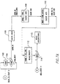
Fig. 4 illustrates, in more detail, one-half of the cache
system in Fig. 3A. In particular, controller 20 is
illustrated along with quadrant Q0 of Cache Module 0 (CACHE
A) and quadrant Q3 in Cache Module 1 (CACHE B). Controller
22, working with quadrants Q1 and Q2 in Cache Modules 0 and
1 respectively, would have the same elements as will now be
described for controller 20 and cache quadrants Q0 and Q3.
The mirror write operation begins with the controller state
machine 24 sending a CACHE REQ (cache request) 0 signal
over line 26 to sync logic 28 in CACHE MODULE 0. At the
same time, controller state machine 24 generates the CACHE
REQ 1 signal, which goes out over line 30 to sync logic 32
in CACHE MODULE 1. The CACHE REQ 0 and CACHE REQ 1 are
shown in the timing diagram illustrated in Fig. 5.
In Fig. 5 the top signal line is the cache address/data
signal indicating the timing of address and data
information on the CDAL (cache data/address line) bus 40 in
Fig. 4. The CACHE REQ 0 and CACHE REQ 1 signals are
represented by a transition from high to low on the signal
lines correspondingly labeled in Fig. 5. These transitions
occur during a time when the address is on the CDAL bus 40
in Fig. 4. Transition 42 of the CACHE REQ 0 signal
notifies CACHE MODULE 0 to read the address on bus 40.
Likewise, transition 44 in CACHE REQ 1 signal notifies
CACHE MODULE 1 to read the cache address on bus 40.
The cache request transitions 42 and 44 also signal the
cache modules to sample the state of the cache read
write/sync signal in Fig. 5. The read write/sync signal is
high to indicate a write and low to indicate a read. As
shown in the mirror write example in Fig. 5, the read
write/sync signal is high at the time of request
transitions 42 and 44. Therefore, both cache modules 0 and
1 will know that data is to be written at the address just
received.
In Fig. 4, as each cache state machine, 37 or 38, accepts
the DATA 0 word unit 39 from CDAL bus 40, the cache state
machine generates an acknowledgment signal, CACHE ACK 0 or
CACHE ACK 1. CACHE ACK 0 goes back from cache state
machine 37 to the sync and latch logic 46 in controller 20.
CACHE ACK 1 goes back from cache state machine 38 to the
sync and latch logic 46 and controller 20.
As shown in Fig. 5, the CACHE ACK 0 and CACHE ACK 1 signals
(negative-going pulses) are not necessarily generated at
the same time. Once both CACHE ACK signals are received at
sync and latch logic 46 in controller 20, AND 48 will
generate an output indicating both cache modules 0 and 1
have acknowledged receipt of the first word unit. This
output goes to the controller state machine 24 which then
drops or transitions the CACHE RW/SYNCH signal (Fig. 5)
from high level to low level. This transition 50 of the
CACHE RW/SYNCH signal in Fig. 5 is the sync signal passed
from the controller state machine back to the cache state
machines 37 and 38. This sync signal tells the cache state
machines that DATA 1 word unit is now on the CDAL bus 40.
In the preferred embodiment, the data on the CDAL bus is in
four data words, data 0, data 1, data 2 and data 3 as shown
in Fig. 5. The data is received and written by the cache
modules starting at the address just previously received
over the CDAL bus and in sequential addresses after the
starting address. At the time the controller places the
last data word unit on the CDAL bus, the controller state
machine raises the CACHE REQ 0 and CACHE REQ 1 signal back
to the high level to indicate the end of the current write
cycle. When these transitions, 52 and 54, occur on the
CACHE REQ signals, the cache state machines are prompted to
acknowledge that the last data is being received.
Accordingly, a CACHE ACK 0 pulse 56 and a CACHE ACK 1 pulse
58 are sent back from the cache state machines to the
controller 20 to acknowledge receipt of data.
Fig. 6, composed of Figs. 6A and 6B, illustrates the
details of the controller state machine 24 of Fig. 4. In
the state flow charts the state machine advances from state
to state on each clock tick from the local clock in the
controller. In addition some states have a decision
operation to detect the presence of a condition before
action is taken and an advance is made to the next state.
The action taken is indicated at the output path of the
state or the decision operation.
In Fig. 6A, start state 51 cooperates with start decision
operation 53 to detect an access request. The access
request is generated by the controller microprocessor in
response to an access request from the host. At each clock
tick, start state 51 causes decision operation 53 to test
for an access request. If there is no access request,
decision operation 53 indicates memory is busy, and the
operation flow returns to start state 51. If there is an
access request detected, decision operation 53 generates a
CDAL ADDR (cache data/address line address) enable signal
to put the address for the access request on the CDAL bus
40 (Fig. 4). The operation flow then passes to CDAL enable
state 55 on the next clock tick.
CDAL enable state 55 keeps the CDAL ADDR enable signal
asserted. On the next clock tick cache request state 57
generates the cache request signals (CACHE_REQ 0 and
CACHE_REQ 1 in Figs 4 and 5). In other words the cache
request signals go through a transition from high to low.
Cache request state 57 also continues to assert the CDAL
enable signal.
Cache access states 59, 61, 63 and 65 are advanced through
in turn in the next successive four clock ticks. Each of
these states maintains the CDAL ADDR enable signal and the
cache request signals. Cache access state 65 also has a
decision operation 66 that tests whether the access request
is a read or write request. If the request is a read
request the operation flow branches to cache read
operations 67 which are not a part of the present invention
and not shown in detail. If the request is a write
request, the CDAL enable signal and the CACHE REQ signal is
generated. The continued assertion of CACHE REQ indicates
there is a cache write request and the last word unit to be
written in this write cycle has not been reached yet. The
operation flow branches to CDAL DATA enable state 68 when
the next clock tick occurs.
CDAL DATA enable state 68 generates the CDAL DATA enable
signal to put data unit words on the CDAL bus 40 (Fig. 4).
State 68 also maintains the cache request signals. For
each clock tick after state 68 the controller state machine
advances through write states 70, 72 and 74. Accordingly,
for these three clock ticks these states maintain the CACHE
REQ signal and the CDAL DATA enable signal.
In state 74, decision operation 76 tests whether the
controller has received back both CACHE ACK 0 and 1 signals
and whether the data word unit to be written is the last
unit in this write cycle to be written. If both of these
conditions are satisfied, this indicates that both cache
modules have acknowledged the write request and that the
controller is sending only one word unit to be written
rather than a burst of four word units. If either of the
conditions is not satisfied, the operation flow branches to
decision operation 77. Decision operation 77 is testing
for receipt of both CACHE ACK 0 and 1 signals and the not
last data word unit, i.e. both cache modules have replied
and a burst of data word units is to be written. If both
decision operation 76 and 77 branch false, then the CACHE
ACK signals must not been received by the controller.
Accordingly, the operation flow branches false back to the
input of write ACK state 74.
The operation flow branches true from decision operation 76
to decision operation 78 when both CACHE ACKs have been
received and only one data word unit has been written.
Decision operation 78 tests whether the word unit to be
written is not the last word unit to be written. Since
decision operation 76 just indicated or detected that it
was the last word unit to be written, the operation flow
will branch false from decision operation 78 to state 80
while maintaining the CDAL data enable condition.
At the next two clock ticks cache write states 80 and 82
maintain the CDAL DATA enable condition. After state 82
and on the occurrence of the next clock tick, cache write
state 84 clears the cache select and the cache request to
prepare for the next access cycle. The operation flow then
returns to the start state 50 in Fig. 6A.
The operation flow branches true from decision operation 77
to operation 86 when both CACHE ACKs have been received and
a burst of four data word units is to be written. Write
sync states 86 and 88 continue to maintain the CDAL data
enable and the cache request signal for the next two clock
ticks. While in state 88 decision operation 78 is again
used to check for the not last condition of the data word
units being sent of the CDAL bus. If the controller
indicates the data word unit is not the last to be written
(burst operation), then the operation flow branches true
from decision operation 78 and the operation maintains the
CACHE REQ signal the CDAL enable and increments the burst
counter. The burst counter will count the number of passes
through the true state detection condition of decision
operation 78 so as to detect when the last data word of a
burst of data words in the write cycle has been placed on
the CDAL bus 40. Thereafter at each clock tick the
operation flow advances through cache write states 90, 92,
94, 96, 98, and 100 successively. Each of these cache
write states maintains the cache request signal in the CDAL
data bus enable condition. Thus, for the next six clock
ticks these conditions are maintained.
After state 100 the operation flow returns to decision
operation 78 to check for the not last condition for data
word units being transmitted over the CDAL bus during this
write cycle. In the preferred embodiment of the invention,
a burst includes four data word units. Accordingly, when
the burst counter indicates the last data word has been put
on to the CDAL bus by the controller decision operation 78
branches false to state 80. As described above, states 80,
and 82 maintain the CDAL data enable condition while the
controller outputs the last data word unit and then state
84 clears the cache selection and cache request in
preparation for the next write cycle.
Cache state machine 37 or 38 in Fig. 4 is illustrated in
detail in Fig. 7, composed of Figs. 7A and 7B. In Fig. 7A,
the operation of the cache state machine begins at start
state 102. Start state 102 includes the start decision
operation 104 and is effectively a wait state waiting for
the receipt of a cache request from the controller. At
each clock tick in the cache module, start decision
operation 104 tests for the cache request signal. When no
cache request signal is present, the operation branches
false from decision operation 104 and stays in the start
state 102. When the cache request signal is present, start
decision operation 104 branches true, and the address
enable condition is initiated at the cache module.
On the next clock tick, cache address state 106 continues
to maintain the address enable condition in the cache
module. Also state 106 increments the burst counter to
count the first data word to be processed in this access
request cycle.
On the next clock tick, CACHE ACK (cache acknowledge) state
108 initiates the CACHE_ACK signal to be passed back from
the cache module to the controller. This confirms that the
cache module has received the access request and the cache
address.
The CACHE_ACK signal is maintained for another clock tick
by state 110. State 110 also enables the ROW COL SEL (row
and column select) condition to enable the address to
select the storage location in the cache module. On the
next clock tick, state 112, the read/write decision state,
includes decision operation 114. Operation 114 tests
whether the access request is a write request. If the
request is a read request, the operation flow branches
false from decision operation 114 to read operations 115.
The read operations are not described herein. However,
note that invention permits reading of either copy of the
mirror written data.
If the access request is a write request, the operation
flow branches true from write decision operation 114 to
write enable state 116 in Fig. 7B. Write enable state 116
is entered on the next clock tick. Notice that the
read/write test state 112 did not maintain the CACHE_ACK
signal, and the CACHE_ACK signal transmitted back to the
controller is ended. In Fig. 7B, the write enable state
116 maintains the ROW COL SEL condition and enables the
writing of the data word unit from the CDAL bus to the
memory address location in the cache chosen to receive by
the cache module. In addition, the write enable state
detects whether this is the last data word unit to be
written in this write cycle. Write enable state 116
enables the CACHE_ACK if the data word is the last data
word unit to be written in the cycle. If the write cycle
is not for a single data word, then CACHE_ACK is not
enabled by state 116. End write state 118 has a decision
operation 120 to detect the not last data word unit
condition. If it is the last data word unit to be written,
the operation branches false from decision operation 120.
On the false condition from operation 120, state 118
maintains the ROW COL SEL condition to finish the writing
of the word, enables the CACHE_ACK signal to indicate to
the controller that the last data word unit is being
written, clears the cache request from the cache module so
that the module is ready to handle the next cache request.
On the next clock tick, memory busy state 122 raises a
memory busy condition and returns the operation flow back
to start state 102 in Fig. 7A to await the next cache
request.
If the data word unit being written in cache is not the
last data word unit in the burst of data word units in the
write cycle, then the operation flow branches true from
decision operation 120. Decision operation 124 then tests
whether a CACHE SYNCH signal is present or being received
from the controller. Since there are two separate cache
state machines, one in each cache module, it is necessary
to sync the cache state machines with the CACHE_RW/SYNCH
signal transition 50 (Fig. 5). If there is no CACHE SYNCH
signal, the operation flow branches false from decision
operation 124 to state 126. The cache state machine will
remain in state 126 until the CACHE SYNCH signal is
detected when a clock tick advances the states in the state
machine. The CACHE SYNCH signal will be received at the
same time by both cache state machines. Accordingly after
state 126, the cache modules proceed in sync. When the
CACHE SYNCH signal is detected, the operation flow branches
true from CACHE SYNCH decision operation 124. In this
event, the burst counter is incremented, and the row column
select condition is raised to select the address location
in the cache for the data to be written. States 128 and
130 maintain the ROW COL SEL condition for two more clock
ticks. On the third clock tick the operation flow returns
to state 116 where the ROW COL SEL condition is maintained
while the data for the data word unit is written by the
write enable state 116. The operation flow in the cache
state machine remains in loop 132 until the last word unit
in the burst of word units to be written has been written.
At that time, the write enable state 116 will raise the
CACHE_ACK, decision operation 120 will branch false
enabling the CACHE_ACK signal for the controller, and then
state 122 memory busy will drop the CACHE_ACK signal and
raise the memory busy signal. This will return the
operation flow back to start state 102 in Fig. 7A.
In the manner described above, the controller will talk to
the cache modules, and the cache modules will respond
whereby the data in the write cycle will be mirror written
to the appropriate quadrant in cache module 0 and cache
module 1.
While the invention has been particularly shown and
described with reference to preferred embodiments thereof,
it will be understood by those skilled in the art that
various changes in the form and details may be made therein
without departing from the invention.