EP0693733A1 - Short-distance communication antennas and methods of manufacture and use of same - Google Patents
Short-distance communication antennas and methods of manufacture and use of same Download PDFInfo
- Publication number
- EP0693733A1 EP0693733A1 EP95304560A EP95304560A EP0693733A1 EP 0693733 A1 EP0693733 A1 EP 0693733A1 EP 95304560 A EP95304560 A EP 95304560A EP 95304560 A EP95304560 A EP 95304560A EP 0693733 A1 EP0693733 A1 EP 0693733A1
- Authority
- EP
- European Patent Office
- Prior art keywords
- antenna
- housing
- communication antenna
- short
- writer
- Prior art date
- Legal status (The legal status is an assumption and is not a legal conclusion. Google has not performed a legal analysis and makes no representation as to the accuracy of the status listed.)
- Granted
Links
Images


Classifications
-
- H—ELECTRICITY
- H01—ELECTRIC ELEMENTS
- H01Q—ANTENNAS, i.e. RADIO AERIALS
- H01Q7/00—Loop antennas with a substantially uniform current distribution around the loop and having a directional radiation pattern in a plane perpendicular to the plane of the loop
-
- H—ELECTRICITY
- H01—ELECTRIC ELEMENTS
- H01Q—ANTENNAS, i.e. RADIO AERIALS
- H01Q7/00—Loop antennas with a substantially uniform current distribution around the loop and having a directional radiation pattern in a plane perpendicular to the plane of the loop
- H01Q7/04—Screened antennas
-
- G—PHYSICS
- G06—COMPUTING; CALCULATING OR COUNTING
- G06K—GRAPHICAL DATA READING; PRESENTATION OF DATA; RECORD CARRIERS; HANDLING RECORD CARRIERS
- G06K19/00—Record carriers for use with machines and with at least a part designed to carry digital markings
- G06K19/06—Record carriers for use with machines and with at least a part designed to carry digital markings characterised by the kind of the digital marking, e.g. shape, nature, code
- G06K19/067—Record carriers with conductive marks, printed circuits or semiconductor circuit elements, e.g. credit or identity cards also with resonating or responding marks without active components
- G06K19/07—Record carriers with conductive marks, printed circuits or semiconductor circuit elements, e.g. credit or identity cards also with resonating or responding marks without active components with integrated circuit chips
- G06K19/077—Constructional details, e.g. mounting of circuits in the carrier
- G06K19/07749—Constructional details, e.g. mounting of circuits in the carrier the record carrier being capable of non-contact communication, e.g. constructional details of the antenna of a non-contact smart card
- G06K19/07773—Antenna details
- G06K19/07777—Antenna details the antenna being of the inductive type
- G06K19/07779—Antenna details the antenna being of the inductive type the inductive antenna being a coil
- G06K19/07781—Antenna details the antenna being of the inductive type the inductive antenna being a coil the coil being fabricated in a winding process
-
- G—PHYSICS
- G06—COMPUTING; CALCULATING OR COUNTING
- G06K—GRAPHICAL DATA READING; PRESENTATION OF DATA; RECORD CARRIERS; HANDLING RECORD CARRIERS
- G06K7/00—Methods or arrangements for sensing record carriers, e.g. for reading patterns
- G06K7/10—Methods or arrangements for sensing record carriers, e.g. for reading patterns by electromagnetic radiation, e.g. optical sensing; by corpuscular radiation
- G06K7/10009—Methods or arrangements for sensing record carriers, e.g. for reading patterns by electromagnetic radiation, e.g. optical sensing; by corpuscular radiation sensing by radiation using wavelengths larger than 0.1 mm, e.g. radio-waves or microwaves
- G06K7/10316—Methods or arrangements for sensing record carriers, e.g. for reading patterns by electromagnetic radiation, e.g. optical sensing; by corpuscular radiation sensing by radiation using wavelengths larger than 0.1 mm, e.g. radio-waves or microwaves using at least one antenna particularly designed for interrogating the wireless record carriers
- G06K7/10336—Methods or arrangements for sensing record carriers, e.g. for reading patterns by electromagnetic radiation, e.g. optical sensing; by corpuscular radiation sensing by radiation using wavelengths larger than 0.1 mm, e.g. radio-waves or microwaves using at least one antenna particularly designed for interrogating the wireless record carriers the antenna being of the near field type, inductive coil
Definitions
- the present invention relates to communication antennas and methods of manufacturing and using the communication antennas. More particularly but not exclusively, this invention relates to a communication antenna for a card reader/writer for transmitting and/or receiving an information signal to and/or from a non-contacting information card using an induced electromagnetic field generated by electromagnetic induction as a transmission medium, and methods of manufacturing and using the communication antenna.
- IC card systems such as automatic ticket examination systems and automatic entrance management systems, have heretofore used a non-contacting information card, such as a management card, and a card reader/writer to transmit information such as an identification (ID) number, an entrance date and an expiry date between the non-contacting information card and the card reader/writer by electromagnetic induction.
- ID identification
- an entrance date an expiry date between the non-contacting information card and the card reader/writer by electromagnetic induction.
- FIG. 1 of the accompanying drawings shows a schematic block diagram of an example of an information card system, such as an automatic ticket examination system, an entrance management system and an IC (integrated circuit) card system.
- an information card system such as an automatic ticket examination system, an entrance management system and an IC (integrated circuit) card system.
- the information card system will be described below with reference to FIG. 1.
- the information card system comprises a card reader/writer 1 and a non-contacting information card 2 which utilizes electromagnetic induction to transmit and receive an information signal between the card and the card reader/writer 1.
- the card reader/writer 1 includes a main control unit 10 comprising a CPU (central processing unit) and a high-order interface controller 11.
- a digital signal comprising transmission information from the main control unit 10 is processed by a P/S (parallel-to-serial) converter 12 in a digital modulation fashion, such as an ASK (amplitude shift keying) modulation or FSK (frequency shift keying) modulation.
- a modulated digital signal output from the P/S converter 12 is supplied to a digital modulator/amplifier 13.
- a digital modulated signal obtained at the output of the digital modulator/amplifier 13 is supplied to a transmission antenna 14.
- a carrier oscillator 15 is connected to the digital modulator/amplifier 13 and generates a carrier signal having a frequency of several hundred kilohertz.
- the card reader/writer 1 includes a reception antenna 16.
- a digital modulated signal received at the reception antenna 16 is supplied to an amplifier/demodulator 17, in which it is amplified and demodulated.
- the demodulated digital signal obtained at the output of the amplifier/demodulator 17 is converted to parallel data by a S/P (serial-to-parallel) converter 18 and supplied to the main control unit 10.
- the non-contacting information card 2 includes a reception antenna 20 which receives the digital modulated signal from the transmission antenna 14 of the card reader/writer 1 by electromagnetic induction.
- FIG. 2 shows an example of transmission and reception of the carrier signal which has a frequency of several hundred kilohertz by electromagnetic induction.
- the transmission antenna 14 may be formed of a loop antenna and a reception antenna 20 may be an antenna having a core. Communication is effected between the loop antenna 14 and the reception antenna 20 by a signal induced at the reception antenna 20 due to the change in a magnetic field generated near the loop antenna 14 by the RF current of several hundred kilohertz supplied to the loop antenna 14.
- the digital modulated signal obtained at the reception antenna 20 is amplified and demodulated by an amplifier/demodulator 21, such as an ASK or FSK demodulator.
- the digital signal obtained at the output of the amplifier/demodulator 21 is converted to parallel data by a S/P (serial-to-parallel) converter 22 and then supplied to a main control unit 23 comprising a CPU.
- main control unit 23 It is determined by the main control unit 23 whether or not information based on the digital signal is a read command signal, a write command signal or write information. Then, the main control unit 23 supplies a predetermined signal to a data memory 24 on the basis of the identified result. Then, information is written in and read out from the data memory 24 under the control of the main control unit 23.
- the digital signal which is read out from the data memory 24 is supplied to the main control unit 23.
- the signal is then output by the main control unit 23 and converted to serial data by a P/S (parallel-to-serial) converter 25, modulated in a digital fashion, such as by ASK modulation, and then amplified by a digital modulator/amplifier 26.
- a digital modulated signal obtained at the output of the digital modulator/amplifier 26 is transmitted to the reception antenna 16 of the card reader/writer 1 via the transmission antenna 27 by electromagnetic induction.
- An oscillator 28 is connected to the digital modulator/amplifier 26 and generates a carrier signal having a frequency of several hundred kilohertz.
- a dotted line block 29 is a battery which supplies the operating voltage for the non-contacting information card.
- the write command signal and the write information signal are supplied to the digital modulator/amplifier 13 from the main control unit 10 of the card reader/writer 1 through the P/S converter 12, digitally modulated and then supplied to the transmission antenna 14.
- the same signal as the signal supplied to the transmission antenna 14 is induced at the reception antenna 20 of the non-contacting information card 2 due to electromagnetic induction.
- the signal thus induced is demodulated to the digital signal of the information signal by the amplifier/demodulator 21 of the non-contacting information card 2.
- the digital signal thus demodulated is converted parallel data by the S/P converter 22 and supplied to the main control unit 23.
- the main control unit 23 identifies the write command signal and the write information signal of the digital signal thus transmitted and writes and stores the write information signal in the data memory 24.
- a digital read command signal is transmitted from the card reader/writer 1 to the non-contacting information card 2 as a digital modulated signal.
- the main control unit 23 of the non-contacting information card 2 detects the read command signal transmitted thereto from the card reader/writer 1. Designated information is read out from the area of the data memory 24 designated by the read command signal. The digital signal thus read out is converted to a serial signal by the P/S converter 25 and digitally modulated by the digital modulator/amplifier 26 which derives a digital modulated signal of this information signal. This digital modulated signal is transmitted to the reception antenna 16 of the card reader/writer 1 through the transmission antenna 27 by electromagnetic induction.
- the digital modulated signal transmitted to the reception antenna 16 is demodulated to produce the digital information signal by the amplifier/demodulator 17. Then, the digital information signal is converted to parallel data by the S/P converter 18. Thus, the information signal of the original digital signal is supplied to the main control unit 10.
- the above information card system uses loop antennas as the transmission antennas 14, 27 to transmit and receive the information signal between the card reader/writer 1 and the non-contacting information card 2 by electromagnetic induction.
- the loop antennas serving as the transmission antennas 14, 27 are sufficiently small as compared with the wavelength. Therefore, since the communication area of the loop antennas 14, 27 is sufficiently small as compared with the wavelength, the electromagnetic field can be approximated by electro-/magneto-static fields.
- the loop antenna 14, for example presents a magnetic field distribution shown in FIG. 3.
- reference numeral 14a denotes a magnetic line of force.
- the communication region becomes symmetrical with respect to front and back, right and left, and up and down.
- the intensity of the radiated magnetic field is restricted to a radiated electromagnetic field intensity obtained within the regulation of the radio law (500 ⁇ v/m at a position 3m distant from the communication region), then the communication distance is limited and communication quality becomes difficult to maintain.
- the loop antenna since the loop antenna is weak in directivity, the loop antenna tends to be easily affected by metal objects near the loop antenna.
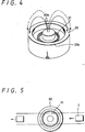
- FIG. 4 shows another example of the transmission antennas 14, 27.
- an antenna wire 31 is wound around a groove portion of a pot core 30 made of a ferromagnetic material.
- a magnetic line of force extends from a central convex core 30a to an outer peripheral annular core 30b as shown by solid lines in FIG. 4.
- leakage magnetic fluxes are generated in all directions and the loop antenna tends to be easily affected by the metal material existing around the loop antenna.
- the non-contacting information card 2 can be scanned from any direction.
- the leakage magnetic flux is generated in all directions, the magnetic flux density received by the non-contacting information card 2 is reduced.
- the pot core 30 which is the magnetic core has to be miniaturized in order to increase the magnetic flux density. There is then the disadvantage that the communication region is reduced.
- a communication antenna provided on a card reader/writer to transmit or transmit and receive an information signal from the card reader/writer to or to and from a non-contacting information card by electromagnetic induction.
- This communication antenna comprises a plurality of magnetic poles disposed on a magnetic member and to and from which a magnetic flux is transmitted and received, and a coil for transmitting or transmitting and receiving the information signal mounted on at least one of the magnetic poles.
- a communication antenna provided on a card reader/writer to transmit or transmit and receive an information signal from the card reader/writer to or to and from a non-contacting information card by electromagnetic induction.
- This communication antenna comprises a housing having an aperture to and from which a magnetic flux is transmitted and received, and a coil for transmitting or transmitting and receiving the information signal mounted on the housing.
- a communication antenna provided on a card reader/writer to transmit or transmit and receive an information signal from the card reader/writer to or to and from a non-contacting information card by electromagnetic induction.
- This communication antenna comprises a housing having an aperture to and from which a magnetic flux is transmitted and received, and a coil formed by winding a conductor around a magnetic member inserted into the inside of the housing.
- a communication antenna provided on a card reader/writer to transmit or transmit and receive an information signal from the card reader/writer to or to and from a non-contacting information card by electromagnetic induction.
- This communication antenna comprises a loop antenna constructing the communication antenna wherein the loop antenna is formed by turning up an antenna conductor in a loop fashion so that currents of opposite directions are flowed to adjacent loop coils.
- a method of manufacturing a communication antenna which comprises the step of winding an antenna conductor around a plurality of bobbins fixed at a predetermined interval while the antenna conductor is alternately reciprocated between the bobbins.
- a communication antenna provided on a card reader/writer to transmit or transmit and receive an information signal from the card reader/writer to or to and from a non-contacting information card by electromagnetic induction.
- This communication antenna comprises an antenna conductor, a conductor pattern having a substrate insulating material on which the antenna conductor and an adjustment strip are formed, wherein conductor patterns formed on both surfaces of the insulating base and connected through a through-hole such that the currents in the adjacent loop antennas flow in opposite directions.
- a method of using a communication antenna wherein the communication antenna is in use, the loop antenna is disposed such that a magnetic flux direction of the antenna is extended along the direction in which the non-contacting information card is moved.
- Embodiments of the present invention provide a communication antenna which is not limited by the inclination angle at which a non-contacting information card is placed in the magnetic flux and which can efficiently transmit electric power, and methods of manufacturing and using the communication antenna.
- a short-distance communication antenna 45 according to a first embodiment of the present invention will be described hereinafter.
- the digital signal of transmission information from the main control unit 10 is converted to serial data by the P/S converter 12 and supplied to the digital modulator/amplifier 13, in which it is modulated in a digital modulation fashion, such as the ASK modulation and then amplified.
- the digital modulated signal obtained at the output side of the digital modulator/amplifier 13 is supplied to the transmission antenna 14.
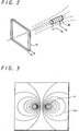
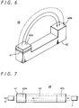
- a short-distance communication antenna 45 such as the transmission antenna 14 of the information card system is arranged as shown in FIGS. 6 and 7.
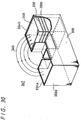
- a magnetic core 40 of U-shaped configuration is made of a ferromagnetic material and includes two magnetic poles 40a, 40b.
- the magnetic core 40 of is disposed such that the two magnetic poles 40a and 40b thereof are laid along a scanning direction a of the non-contacting information card 2 as shown in FIG. 7.
- an antenna wire 41 is wound around the magnetic pole 40a of the magnetic core 40.
- the digital modulated signal obtained at the output side of the digital modulator/amplifier 13 is supplied to the antenna wire 41.
- the direction connecting the two magnetic poles 40a and 40b of the magnetic core 40 is set to the scanning direction a . Also, a predetermined surface of the non-contacting information card 2 arranged as shown in FIG. 2 is opposed to the antenna 45.
- a main magnetic flux and a leakage magnetic flux generated from the antenna wire 41 are generated only in the scanning direction a of the non-contacting information card 2 which is placed between the magnetic poles 40a and 40b as shown by a solid line and a dotted line in FIG. 6. Since intensity of this magnetic field has a directivity, a leakage of magnetic flux to the outside of the communication area is small and therefore the communication area can be extended within the regulation range of the radio law, thereby making it possible to satisfactorily transmit and receive information. Also, since the leakage of magnetic flux is small, the communication can be substantially prevented from being affected by a metal material existing near the communication antenna.
- the intensity of magnetic field has a directivity in the scanning direction a of the non-contacting information card 2
- a magnetic flux density can be improved and a transmission and reception efficiency can be improved.
- the magnetic core of U-shaped configuration having the two magnetic poles 40a, 40b is used as the magnetic core 40 as described above, the magnetic core may have three magnetic poles or more disposed along one direction. In this case, if the magnetic core has four magnetic poles or more, the antenna wire 41 should preferably be wound around a plurality of magnetic poles.
- the leakage of magnetic flux to the outside of the communication area is small, the satisfactory transmission and reception can be made within the regulation range of the radio law. Also, since the leakage of magnetic flux is small, the communication can be substantially prevented from being affected by the metal material existing near the communication antenna.
- the intensity of magnetic field has a directivity in the scanning direction of the non-contacting information card, the magnetic flux density can be improved and therefore the transmission and reception efficiency can be improved.
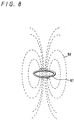
- annular loop antenna 51 shown in FIG. 8 is used as the comparative example of the communication antenna for the card reader/writer 1 shown in FIG. 1, then the loop antenna 51 generates a magnetic flux 52 which encircles the loop of the loop antenna 51 as shown by a dotted line in FIG. 8.
- the non-contacting information card 2 is placed in parallel to the loop antenna 51 as shown in FIG. 9A, then electric power can be transmitted most efficiently between the card reader/writer 1 and the non-contacting information card 2. However, it is substantially impossible for the non-contacting information card 2 to constantly communicate with the communication card 2 at such position.
- a communication antenna according to an second embodiment of the present invention which can satisfy the above demand will be described below.
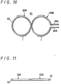
- FIG. 10 is a plan view and FIG. 11 is a cross-sectional view each showing a communication antenna for the card reader/writer 1, i.e., short-distance communication antenna which serves as the transmission antenna 14 and the transmission and reception antenna 16 according to the second embodiment of the present invention.
- a communication antenna for the card reader/writer 1 i.e., short-distance communication antenna which serves as the transmission antenna 14 and the transmission and reception antenna 16 according to the second embodiment of the present invention.
- the short-distance communication antenna 61 includes two adjacent loop coils 63A and 63B which are formed by turning an antenna conductor 62 up in a loop fashion so as to cross each other at its intermediate portion, i.e., in the shape of the infinity symbol, in a plane.
- a current i flows in the opposite directions.
- Feeding terminals 64A and 64B are led from the respective ends of the antenna conductor 62.
- a magnetic flux 65 generated from one loop coil 63A is returned to the adjacent loop coil 63B. Accordingly, the magnetic flux 65 is closed at portions 66 and 67 corresponding to the portion between the adjacent loop coils 63A and 63B. Further, the magnetic flux 65 is multiplied with magnetic fluxes generated from the left and right loop coils 63A and 63B so that the magnetic flux densities of the portions 66 and 67 increase. Therefore, a sufficient induced voltage can be generated in the non-contacting information card 2 disposed within the two portions 66 and 67 by electromagnetic induction.
- the non-contacting information card 2 Upon communication, the non-contacting information card 2 is moved over the portion 66 or 67 with an inclination angle with respect to the antenna 61. In this case, since the magnetic flux 65 of the antenna 61 is closed, the non-contacting information card 2 can reliably communicate with the card reader/writer 1 regardless of the direction, i.e., inclination angle of the non-contacting information card 2 relative to the antenna 61.
- the non-contacting information card 2 when the non-contacting information card 2 is placed at a right angle relative to the plane of the loop antenna 61 (which is the short-distance communication antenna) on the portion 66 or 67 (portion 66 in FIG. 12) as shown by a solid line in FIG. 12 or when the non-contacting information card 2 is placed in parallel to the plane of the loop antenna 61 as shown by a two-dot chain line in FIG. 12, in any cases, the card reader/writer 1 and the non-contacting information card 2 can reliably communicate with each other.
- the transmission efficiency of electric power can be improved as compared with an antenna having a single loop.
- the operation area of the non-contacting information card 2 can be limited to only the areas of the portions 66 and 67 corresponding to the area between the adjacent loop coils 63A and 63B.
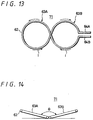
- FIG. 13 is a plan view and FIG. 14 is a cross-sectional view each showing a short-distance communication antenna 71 according to a third embodiment of the present invention.
- the short-distance communication antenna 71 includes two adjacent loop coils 63A and 63B which are formed by turning an antenna conductor 62 up in a loop fashion so as to cross each other at its intermediate portion, i.e., in the shape of the infinity symbol, as shown in a plan view of FIG. 13 similarly to FIG. 10.
- the two loop coils 63A and 63B are bent such that an angle ⁇ formed by the two loop coils 63A and 63B is smaller than 180°.
- the communication antenna 71 has a directivity so that the operation area of the non-contacting information card 2 can be reduced. Moreover, the for installing the communication antenna 71 can be reduced.
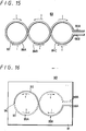
- FIG. 15 is a plan view showing a short-distance communication antenna 83 according to a fourth embodiment of the present invention.
- the short-distance communication antenna 83 includes more than two , in this embodiment, three adjacent loop coils 84A, 84B and 84C which are formed by winding a single antenna conductor 62 in a loop fashion.
- a current i flows in opposite directions.
- the feeding terminals 64A and 64B are led out from the respective ends of the antenna conductor 62.
- a magnetic flux generated from the central loop coil 84B is returned to the respective loop coils 84A and 84C that adjoin the central loop coil 84B. Accordingly, the magnetic fluxes are closed in the areas corresponding to the crossing portions of the antenna conductor 62 between the adjacent loop coils 84A and 84B and the adjacent loop coils 84B and 84C. As a result, the area of high magnetic flux density is expanded so that the operation area of the non-contacting information card 2 can be extended by an arbitrary distance. That is, the operation area of the non-contacting information card 2 can be enlarged.
- loop coil 84A and 84C are wound by one turn, only the loop coil 84B is wound by two turns.
- the ratio of the turns of loop coil 84A : loop coil 84B : loop coil 84C can be set to 1 : 2 : 1.
- FIG. 16 is a plan view and FIG. 17 is a perspective view each showing a short-distance communication antenna according to a fifth embodiment of the present invention.
- the short-distance communication antenna 90 includes an insulating base 91, a conductor pattern 92 of an inverted S- shape serving as an antenna conductor formed on an upper surface 91a of the insulating base 91 and a conductor pattern 93 of an inverted S- shape serving as an antenna conductor formed on a lower surface 91b of the base 91 so as to cross the conductor pattern 92 of the inverted S-shape formed on the upper surface 91a at its intermediate portion.
- One end of the conductor patterns 92 and 93 are connected via a through-hole 94.
- the two conductor patterns i.e., the antenna conductor patterns 92 and 93 form two adjacent loop coils 95A and 95B in which the current i flows in the opposite directions as shown in a plan view of FIG. 16.
- Feeding terminals 96A and 96B formed of conductor patterns are led out from the respective ends of the loop coils 95A and 95B.
- a sufficient induced voltage can be generated in the non-contacting information card 2.
- the card reader/writer 1 and the non-contacting information card 2 can reliably communicate with each other regardless of the inclination angle of the non-contacting information card 2 relative to the plane of the communication antenna 90.
- FIG. 18 is a plan view showing a short-distance communication antenna according to a sixth embodiment of the present invention.
- the short-distance communication antenna 100 differs from the short-distance communication antenna 90 only in that a plurality of adjustment strips (metal foil strips) 101 are formed on the upper surface 91a of the insulating base 91 together with the conductor patterns, i.e., antenna conductor patterns 92 and 93.
- the short-distance communication antenna 100 can achieve action and effect similar to those of the short-distance communication antenna 90 of the example shown in FIG. 16, since the short-distance communication antenna 100 includes the adjustment strips 101, the influence exerted upon devices disposed around the antenna can be removed and fluctuations brought when the antenna conductor patterns 92, 93 are manufactured can be corrected.
- the adjustment can be carried out with ease by properly removing the adjustment strip 101.
- the antenna conductor patterns 92, 93 or the adjustment strips 101 shown in FIGS. 16 and 18 can be formed by treating conductive foils or conductive layers deposited on the insulating base 91 by chemical selective etching. According to the short-distance communication antennas 90 and 100, the antenna conductor patterns 92, 93 or the adjustment strips 101 can be placed and sized with high accuracy by chemical etching. Therefore, a number of loop coils 95A, 95B of the same size can be formed at predetermined positions and are suitable for being mass-produced.
- the loop coils 95A, 95B are composed of the conductor patterns 92, 93 formed on both surfaces 91a, 91b of the insulating base 91, the two loop coils 95A, 95B can be manufactured with high accuracy in compact. Also, the short-distance communication antenna can be located with ease.
- While the two loop coils 95A and 95B are formed in the examples of FIGS. 16 and 18 as described above, three loop coils or more may be formed.
- loop coils 63A, 63B, 84A, 84B, 84C, 95A and 95B are each shaped as a proper circle as shown in the plan views, they may be each shaped as any suitable shape, such as an oblong ellipse or a rectangle.
- the antenna conductors 62 shown in FIGS. 10, 13 and 15 are formed of a line-shaped antenna wire and therefore can be wound many times around the thickness direction of the antenna.
- a winding apparatus 204 including a common base 201 on which a pair of bobbins 202, 203 are disposed with a predetermined spacing therebetween in an opposing relation.
- An antenna conductor is wound around the pair of bobbins 202, 203 of the winding apparatus 204 in an S- shape, for example, manually.
- the antenna conductor is alternately wound around the two bobbins 202, 203 in the opposite directions such that the antenna conductor is wound around the left bobbin 202 in the counter-clockwise direction around the right bobbin 203 in the clockwise direction.
- winding apparatus 204 By using the winding apparatus 204, it is possible to manufacture with ease the short-distance communication antenna 61 shown in FIG. 10, for example, manually.
- the antenna conductor When a frequency at which the antenna conductor overlaps at the crossing portion between the left and right antenna loops is reduced, after the antenna conductor is wound around the left bobbin 202 a plurality of times (e.g., twice or greater) as a unit, the antenna conductor is wound around the right bobbin 203 the same number, thereby making it possible to manufacture the target short-distance communication antenna.
- an automatic winding machine 209 comprises the winding apparatus 204 shown in FIGS. 19A to 19C mounted on a work table 206 such that the winding apparatus 204 can be reciprocated only in one direction. Also, this automatic winding machine 209 includes a rotary arm 208 attached thereto having an antenna conductor supply head (i.e., so-called winding head) 207 which is mounted on the work table 206. As shown in FIG.
- the rotary arm 208 can be rotated about a rotary shaft 210 such that the rotary arm 208 reciprocates in the direction crossing a reciprocating direction b of the winding apparatus 204, i.e., in a direction c perpendicular to the reciprocating direction b .
- the antenna conductor 62 is moved along the rotary arm 208 and supplied to the antenna conductor supply head 207 attached to the rotary arm 208.
- the antenna conductor 62 is wound around the bobbins 202, 203 of the winding apparatus 204 in an S- shape, thus to make, for example, the short-distance communication antenna 61 of FIG. 10 composed of the two loop coils 63A, 63B.
- the antenna conductor 62 may of course be wound around the bobbins 202, 203 a plurality of times.
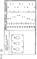
- FIG. 22 shows the order wherein the antenna conductor supply head 207 is operated.
- the order wherein the antenna conductor supply head 207 is operated and the positions thereof are illustrated by (1) through (8).
- a column (A) shows the positions at which the antenna conductor supply head 207 is placed in the sequential order when the antenna conductor supply head 207 is operated in accordance with the left and right movement of the winding apparatus 204 in the direction b .
- a column (B) shows positions at which the antenna conductor supply head 207 is placed in the sequential order when the antenna conductor supply head 207 is operated in accordance with the rotational displacement of the rotary arm 208 in the direction c .
- the movement amount or the rotational displacement amount is large.
- the antenna conductor supply head 207 and the winding apparatus 204 are placed side by side (e.g., (2) and (3) in the column (A) and (1) and (2) in the column (B)), the movement amount or the rotational displacement amount is small.
- the automatic winding machine 209 shown in FIGS. 20 and 21 if a power source of the winding apparatus 204 and the rotary arm 208 is formed of a suitable motor, such as a stepping motor which operates in a straight line fashion, then the automatic winding machine can be made simple and inexpensive. Moreover, the loop coils whose winding types, such as one turn or two turns are different can be switched with ease, which is very economical.
- FIGS. 23A to 23C and FIG. 24 show a further example of method of manufacturing a short-distance communication antenna composed of three loop coils.
- FIGS. 23A to 23C there is prepared a winding apparatus 215 having a common base 211 on which three bobbins 212, 213, 214 are arrayed with a predetermined spacing between adjacent ones.
- This winding apparatus 215 is mounted on the automatic winding machine 209 shown in FIGS. 20 and 21 instead of the winding apparatus 204.
- the table of FIG. 24 is constructed in the same way as that of the table of FIG. 22 and therefore need not be described in detail.
- the ratio of the number of the turns of the antenna conductor wound on the bobbins 212, 213, 214 is set to 1 : 1 : 1.
- the antenna conductor 62 is wound around the bobbins 212, 213, 214 repeatedly twice only in the operation orders (1) to (4), then of the three loop coils thus made, the number of turns of the central loop coil becomes twice those of the left and right loop coils. With this arrangement of the loop coils, the amount of generated magnetic fluxes can be well balanced.
- the portion in which the magnetic flux is closed is formed by forming a plurality of loop coils. Moreover, the magnetic flux density of that portion increases due to the synergism of the magnetic flux from the adjacent loop coil, thereby making it possible for the card reader/writer 1 and the non-contacting information card 2 to communicate with each other satisfactorily. Also, regardless of the direction (inclination) of the non-contacting information card 2 upon reception, it is possible for the non-contacting information card 2 to efficiently receive the magnetic field accompanied with the information signal.
- the direction of the non-contacting information card can be freely selected relative to the communication antenna of the card reader/writer.
- a short-distance communication antenna includes a metal housing having one or more than two apertures through which a magnetic flux is passed and a coil mounted on this metal housing, i.e., antenna coil.
- the housing should be made of a conductor, preferably a metal material and more preferably a copper plate.
- the material of the housing is not limited thereto so longas the material has a shield function.
- a slit is formed through the housing so as to join the apertures each other.
- the size and a shape of the housing are not limited in particular. If the housing is U-shaped or E-shaped, magnetic flux is easily closed in one direction. Moreover, the magnetic flux direction of the antenna is extended along the direction wherein the non-contacting information card is moved. Thus, communication range can be enlarged.
- a magnetic member (magnetic core) can be inserted into the inside of the housing.
- the magnetic member can be inserted into a part or whole of the housing.
- the magnetic member might generally be a ferrite core and the shape of the magnetic member is not limited so long as it can be inserted into the inside of the housing.
- the coil there can be used a coil formed by winding a conductor, a coil formed by winding a conductor around a bobbin, a coil formed by winding a conductor around a magnetic core and a coil formed by etching a conductor as a spiral coil.
- the coil should preferably be formed by winding a flat type wire conductor without a space.
- the digital signal of transmission information from the main control unit 10 is converted to serial data by the P/S converter 12 and supplied to the digital modulator/amplifier 13, in which it is processed in a digital modulation fashion, such as the ASK modulation and then amplified.
- the modulated wave obtained at the output side of the digital modulator/amplifier 13 is supplied to the transmission antenna 14.
- the transmission antenna 14 and the reception antenna 16 in the card reader/writer 1 shown in FIG. 1 can be formed of a single antenna which serves as both the transmission and reception antennas.
- the reception antenna 20 and the transmission antenna 27 in the non-contacting information card 2 can be formed of a single antenna which serves as both the transmission and reception antennas.
- the transmission and reception antenna on the non-contacting information card 2 can be formed by etching a metal thin film or metal foil.
- the present invention is applied to a short-distance communication antenna which becomes the transmission antenna 14 or the transmission and reception antenna serving as both the transmission antenna 14 and the reception antenna 16 of this information card system.
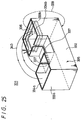
- FIG. 25 shows a short-distance communication antenna according to a seventh embodiment of the present invention.
- a short-distance communication antenna 331 comprises a metal housing 335 of U- shaped cylinder configuration in which upper end faces of vertical portions 333a, 333b extended from respective ends of a horizontal portion 332 in the vertical direction are formed as apertures 334a, 334b and a transmission and reception coil (i.e., so-called antenna coil) 336 mounted on the housing 335.
- the housing 335 is formed of a metal having a magnetic shield function, i.e., non-magnetic conductor, e.g., copper.
- This housing 335 becomes a conductive magnetic cylinder for introducing a magnetic flux generated from the antenna coil 336 along the inside of the housing 335.
- the housing 335 is made at its portion where the magnetic flux travels by an air or plastic material and the portion surrounding that portion is surrounded by a metal plate.
- the coil 336 is wound around the inner peripheral surface of one vertical portion 333b of the housing 335.
- the coil 336 can be mounted in other positions within the housing 335 or can be wound around the outside of the housing 335.
- the cylindrical housing 335 includes a short-circuit circuit crossing a magnetic path formed by the coil 336, i.e., a slit (groove) 337 in order to prevent currents i1, i2, i3 from being induced.
- the slit 337 is extended over the whole length of the conductive magnetic cylinder of inside U- shaped configuration extended over the horizontal portion 332 and the two vertical portions 333a, 333b joining the two apertures 334a and 334b.
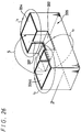
- the coil 336 disposed within the metal housing 335 generates a magnetic flux accompanied with the information signal in all directions.
- the magnetic flux is generally classified as a magnetic flux S which is generated from one aperture 334a to the outside of the housing 335 and returned from the other aperture 334b to the inside of the housing 335 and a magnetic flux P which tends to pass the metal plate of the housing 335.
- a component R which is perpendicular to the metal plate of the housing 335 generates an eddy current in the metal plate of the housing 335.
- a magnetic flux -R generated by the eddy current is generated in the direction to cancel the original magnetic flux R.
- the metal plate of the housing 335 acts as a diamagnetic material to remove the magnetic flux R which passes the metal plate of the housing 335.
- most of the magnetic flux P becomes a component Q that flows along the metal plate of the housing 335.
- the magnetic fluxes generated by the coil 336 form a magnetic path which passes the inside of the housing 335, i.e., the conductive magnetic cylinder, extends from one aperture 334a to the outside of the housing 335 and which returns from other aperture 334b to the inside of the housing 335.
- the magnetic flux is closed and therefore a harmful leakage flux can be substantially suppressed.
- the housing 335 formed of the metal plate capable of magnetic shielding can avoid the occurrence of the harmful leakage magnetic flux 339 which flows to the rear surface of the housing 335 from the aperture 334b.
- the main magnetic flux 340 accompanied with the information signal generated from the coil 336 is generated only in the direction between the two apertures 334a and 334b. Moreover, since this magnetic field intensity has a directivity, the communication area can be secured sufficiently within the regulation range of the radio law and the leakage magnetic flux flowed to the outside of the communication area can be suppressed, thus to obtain a high performance antenna which can be substantially prevented from interfering the conductor (e.g., metal material) disposed near the antenna.
- the conductor e.g., metal material
- the antenna becomes very light and inexpensive.
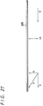
- the short-distance communication antenna 331 is disposed in use such that the magnetic flux direction of antenna between the apertures 334a and 334b is extended along the moving direction a of the non-contacting information card 2 shown in FIG. 1.
- the short-distance communication antenna 331 is disposed along the moving direction a of the non-contacting information card 2, then the communication area can be extended.
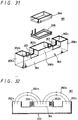
- FIG. 30 shows a short-distance communication antenna 347 according to an eighth embodiment of the present invention.
- the short-distance communication antenna 347 differs from the short-distance communication antenna 331 shown in FIG. 25 only in that a part or whole of the magnetic circuit disposed within the housing 335 of U-letter configuration having the two apertures 334a and 334b is replaced with a magnetic member, e.g., ferrite core 348.
- a magnetic member e.g., ferrite core 348.
- the rectangular parallelpiped ferrite core 348 around which the coil 336 is wound is inserted into one vertical portion 333b of the housing 335.
- the ferrite core 348 is inserted into the magnetic circuit composed of the housing 335 of U-shaped configuration, as compared with the short-distance communication antenna 331 shown in FIG. 25, the magnetic resistance of the magnetic circuit can be reduced more, the magnetic flux can pass the housing 335 more easily and the harmful leakage magnetic flux can be reduced more. Thus, a radiation efficiency of the main magnetic flux can be improved.
- the ferrite core 348 is magnetically shielded by the metal housing 335, it is possible to suppress the undesired harmful leakage magnetic flux generated from the ferrite core 348. Since the ferrite core 348 is inserted into the housing 335, it is possible to obtain a high performance antenna of high efficiency which can be prevented from interfering with the nearby conductor though the antenna becomes a little heavy.
- the amount of the inserted ferrite core 348 is selected in accordance with performance, weight and cost in actual practice, then it is possible to obtain the proper short-distance communication antenna of high quality which has less harmful leakage magnetic flux.
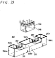
- FIGS. 31 and 32 show a short-distance communication antenna according to a ninth embodiment of the present invention.
- the short-distance communication antenna 351 includes a metal housing formed of E-shaped cylinder having three apertures 352a, 352b, 352c, i.e., a housing 353 having a horizontal portion 355 and vertical portions 356a, 356b, 356c vertically extended from respective ends and the center of the horizontal portion 355 and in which end faces of the vertical portions 356a, 356b and 356c are formed as the apertures 352a, 352b, 352c and a coil bobbin 354 around which a coil 336 is wound is inserted into the housing 353, i.e., the vertical portion 356b having the central aperture 352b in this embodiment.
- the housing 353 of E-shaped configuration is formed of a metal plate similar to that of the aforementioned housing 335.
- the housing 353 also includes slits (grooves) 357 formed through the vertical portions 356a, 356b, 356c and the horizontal portion 355 to join the apertures 352a and 352b and the apertures 352b and 352c in order to avoid the short-circuit crossing the magnetic path similarly as described above.
- the magnetic fluxes 350a and 350b that are generated by the coil 336 form the magnetic path which extends from the central aperture 352b of the housing 353 to the outside of the housing 353 and which also returns from the apertures 352a and 352b of the respective ends of the housing 353 to the inside of the housing 353 to thereby close the magnetic fluxes 350a and 350b.
- the harmful leakage magnetic flux can be suppressed similarly to the embodiment shown in FIG. 25.
- the main magnetic fluxes 350a, 350b generated from the coil 336 are generated only in the directions between the central aperture 352b and other apertures 352a, 352c of the respective ends of the housing 353.
- FIG. 33 shows a short-distance communication antenna according to a tenth embodiment of the present invention.
- a short-distance communication antenna 357 according to the tenth embodiment differs from the short-distance communication antenna 351 shown in FIG. 31 only in that the coil 336 wound around the coil bobbin 354 is replaced with such one that results from winding the coil 336 around a magnetic member, i.e., ferrite core 348 and that this one is inserted into the central vertical portion 356b from the central aperture 352b.
- a magnetic member i.e., ferrite core 348
- the magnetic flux can pass the magnetic circuit more easily, the magnetic resistance can be lowered, the harmful leakage magnetic flux can be reduced more and the radiation efficiency of the main magnetic flux can be improved.
- the magnetic member inserted into the housing 353, e.g., the ferrite core 348 there can be used magnetic members of various shapes. Specifically, if the amount of the inserted ferrite core 348 is selected in accordance with performance, weight and cost in actual practice, then it is possible to obtain the proper antenna of excellent quality which does not generate a harmful leakage magnetic flux substantially.
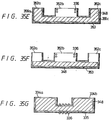
- Examples of the ferrite core 348 will be described with reference to FIGS. 34A through 34D and FIGS. 35E to 35G.
- FIG. 34A shows an example wherein the ferrite core 348 with the coil 336 wound therearound is disposed only within the central vertical portion 356b of the housing 353 of E-shaped configuration.
- FIG. 34B shows an example wherein the ferrite core 348 with the coil 336 wound therearound is disposed in the portion to the bottom surface of the horizontal portion 355 from the upper surface of the central vertical portion 356b.
- FIG. 34C shows an example wherein the ferrite core 348 with the coil 336 wound therearound is disposed in the portion to the bottom surface of the horizontal portion 355 from the upper surface of the central vertical portion 356b and ferrite cores 348 having no coils 336 wound therearound are disposed on the portion to the bottom surface of the horizontal portion 355 from the upper surface of the vertical portions 356a, 356c of the respective ends of the housing 353 of E-shaped configuration, respectively.
- FIG. 34D shows an example wherein the ferrite core 348 of E-shaped configuration is disposed so as to completely fill the housing 353 Incidentally, the coil 336 is wound around the central protruded portion of the ferrite core 348.
- FIG. 35E shows an example wherein the ferrite core 348 of U-shaped configuration that is joined with the vertical portions 356a, 356c of the respective ends of the housing 353 and the horizontal portion 335 is disposed within the housing 353.
- FIG. 35F shows an example wherein the ferrite core 348 is disposed only on the horizontal portion 355 within the housing 353.
- a coil 336 is wound on the inner surface of the central vertical portion 356b.
- FIG. 35G shows an example wherein the ferrite core 348 of U-shaped configuration is disposed within the housing 335 shown in the example of FIG. 25.
- the coil 336 also is not wound on the inner surface of the housing 335 but can be wound around the outside of the housing 335.
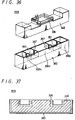
- FIGS. 36 and 37 show a short-distance communication antenna 359 according to an eleventh embodiment of the present invention.
- the short-distance communication antenna 359 includes a housing 360 of E-shaped configuration in which side surfaces of spacings 361 formed between the central vertical portion 356b and left and right end vertical portions 356a and 356c are closed.
- the coil 336 is mounted in the housing 360.
- the E-shaped ferrite core 348 with the coil 336 wound around its central protruded portion is inserted into the inside spacing of the housing 360.
- the short-distance communication antenna 359 since its housing 360 has a continuous rectangular parallelpiped structure as seen from the outside, it is possible to suppress the leakage magnetic flux much more as compared with the case that the short-distance communication antenna includes the housing 353 of E-shaped configuration.
- the short-distance communication antenna 359 according to this embodiment can achieve similar action and effects to those of the short-distance communication antennas shown in FIGS. 31 and 33.
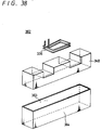
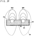
- FIG. 38 and 39 show a short-distance communication antenna 362 according to a twelfth embodiment of the present invention.
- the short-distance communication antenna 362 comprises a metal housing 364 of a rectangular parallelpiped structure having an aperture 363 defined on the upper surface of the housing 364 and an E- shaped magnetic member, i.e., ferrite core 348 having a coil 336 wound around its central protruded portion inserted into the housing 364.
- the housing 364 is formed of a metal plate similar to the metal plate which forms the aforementioned housing 335.
- magnetic fluxes 365a, 365b generated by the coil 336 form a magnetic paths which extend from the center of the opening portion 336 to the outside of the housing 364 and which return from the respective ends of the opening portion 363 to the inside of the housing 364.
- the magnetic fluxes 365a, 365b are closed.
- a harmful leakage magnetic flux 366 can be shielded by the housing 364 and is not generated. Accordingly, it is possible to obtain the antenna wherein the leakage magnetic flux to the outside of the communication area is small and the interference to the conductors provided near the antenna is small while the communication area can be secured sufficiently similarly as described above.
- the short-distance communication antenna according to this embodiment can be applied to the case that a disturbance of an internal magnetic path is small and that a remarkable bad influence is not exerted upon characteristics.
- the housings of the respective embodiments are formed of a thin copper plate, for example, though not shown, in order to improve a mechanical strength thereof, it is possible to form the housing as a double-structure by covering the outside of the housing with a mechanically strong iron material.
- the magnetic flux direction of the antenna is extended along the moving direction a of the non-contacting information card 2 similarly to FIG. 29.
- the communication area can be extended.
- a flat type wire coil 464 shown in FIG. 40 is preferable rather than a round type wire coil 461 shown in FIG. 41.
- the reason for this is as follows. That is, since a length of a magnetic path of a local magnetic flux 370 generated in a conductor of one turn of the flat type wire coil 462 is long as compared with that of the round type wire coil 461, a magnetic resistance increases and the local magnetic flux 370 decreases. Moreover, in the case of the flat type wire coil 462, the local magnetic fluxes 370 cancel each other out between adjacent conductors and become small.
- reference numeral 371 depicts a main magnetic flux.
- the short-distance communication antenna since the magnetic flux accompanied with the information signal is closed, the communication area can be maintained sufficiently and the leakage magnetic flux leaked to the outside of the communication area can be reduced by the metal housing. Therefore, satisfactory transmission and reception can be carried out within the regulation range of the radio law. Moreover, the leakage magnetic flux is small and therefore the interference on the conductors disposed near the antenna is small.
- the magnetic field intensity has a directivity
- the magnetic flux density is improved and also the transmission and reception efficiency can be improved
- a magnetic resistance of a magnetic circuit formed within the housing can be reduced and an efficiency with which the antenna radiates a magnetic flux can be improved.
- the coil which is formed by winding a conductor around a magnetic member, is inserted into the housing, a magnetic flux generated from the coil passes the magnetic member. Therefore, the leakage magnetic flux can be suppressed much more and the magnetic resistance becomes small. Thus, it is possible to improve an efficiency with which the antenna radiates a magnetic flux.
- the short-distance communication antenna when using the short-distance communication antenna, it is possible to extend the communication area by disposing the short-distance communication antenna such that the magnetic flux direction of the antenna is extended along the moving direction of the non-contacting information card.
Abstract
Description
- The present invention relates to communication antennas and methods of manufacturing and using the communication antennas. More particularly but not exclusively, this invention relates to a communication antenna for a card reader/writer for transmitting and/or receiving an information signal to and/or from a non-contacting information card using an induced electromagnetic field generated by electromagnetic induction as a transmission medium, and methods of manufacturing and using the communication antenna.
- IC card systems, such as automatic ticket examination systems and automatic entrance management systems, have heretofore used a non-contacting information card, such as a management card, and a card reader/writer to transmit information such as an identification (ID) number, an entrance date and an expiry date between the non-contacting information card and the card reader/writer by electromagnetic induction.
- FIG. 1 of the accompanying drawings shows a schematic block diagram of an example of an information card system, such as an automatic ticket examination system, an entrance management system and an IC (integrated circuit) card system. The information card system will be described below with reference to FIG. 1.
- As shown in FIG. 1, the information card system comprises a card reader/
writer 1 and anon-contacting information card 2 which utilizes electromagnetic induction to transmit and receive an information signal between the card and the card reader/writer 1. - As shown in FIG. 1, the card reader/
writer 1 includes amain control unit 10 comprising a CPU (central processing unit) and a high-order interface controller 11. A digital signal comprising transmission information from themain control unit 10 is processed by a P/S (parallel-to-serial)converter 12 in a digital modulation fashion, such as an ASK (amplitude shift keying) modulation or FSK (frequency shift keying) modulation. A modulated digital signal output from the P/S converter 12 is supplied to a digital modulator/amplifier 13. A digital modulated signal obtained at the output of the digital modulator/amplifier 13 is supplied to atransmission antenna 14. Acarrier oscillator 15 is connected to the digital modulator/amplifier 13 and generates a carrier signal having a frequency of several hundred kilohertz. - The card reader/
writer 1 includes areception antenna 16. A digital modulated signal received at thereception antenna 16 is supplied to an amplifier/demodulator 17, in which it is amplified and demodulated. The demodulated digital signal obtained at the output of the amplifier/demodulator 17 is converted to parallel data by a S/P (serial-to-parallel)converter 18 and supplied to themain control unit 10. - The
non-contacting information card 2 includes areception antenna 20 which receives the digital modulated signal from thetransmission antenna 14 of the card reader/writer 1 by electromagnetic induction. FIG. 2 shows an example of transmission and reception of the carrier signal which has a frequency of several hundred kilohertz by electromagnetic induction. - As shown in FIG. 2, the
transmission antenna 14 may be formed of a loop antenna and areception antenna 20 may be an antenna having a core. Communication is effected between theloop antenna 14 and thereception antenna 20 by a signal induced at thereception antenna 20 due to the change in a magnetic field generated near theloop antenna 14 by the RF current of several hundred kilohertz supplied to theloop antenna 14. - Referring back to FIG. 1, the digital modulated signal obtained at the
reception antenna 20 is amplified and demodulated by an amplifier/demodulator 21, such as an ASK or FSK demodulator. The digital signal obtained at the output of the amplifier/demodulator 21 is converted to parallel data by a S/P (serial-to-parallel)converter 22 and then supplied to amain control unit 23 comprising a CPU. - It is determined by the
main control unit 23 whether or not information based on the digital signal is a read command signal, a write command signal or write information. Then, themain control unit 23 supplies a predetermined signal to adata memory 24 on the basis of the identified result. Then, information is written in and read out from thedata memory 24 under the control of themain control unit 23. - The digital signal which is read out from the
data memory 24 is supplied to themain control unit 23. The signal is then output by themain control unit 23 and converted to serial data by a P/S (parallel-to-serial)converter 25, modulated in a digital fashion, such as by ASK modulation, and then amplified by a digital modulator/amplifier 26. A digital modulated signal obtained at the output of the digital modulator/amplifier 26 is transmitted to thereception antenna 16 of the card reader/writer 1 via thetransmission antenna 27 by electromagnetic induction. Anoscillator 28 is connected to the digital modulator/amplifier 26 and generates a carrier signal having a frequency of several hundred kilohertz. In FIG. 1, a dotted line block 29 is a battery which supplies the operating voltage for the non-contacting information card. - Since the information card system is arranged as described above, when information is written in the non-contacting information card, initially, the write command signal and the write information signal are supplied to the digital modulator/
amplifier 13 from themain control unit 10 of the card reader/writer 1 through the P/S converter 12, digitally modulated and then supplied to thetransmission antenna 14. - The same signal as the signal supplied to the
transmission antenna 14 is induced at thereception antenna 20 of thenon-contacting information card 2 due to electromagnetic induction. The signal thus induced is demodulated to the digital signal of the information signal by the amplifier/demodulator 21 of thenon-contacting information card 2. Then, the digital signal thus demodulated is converted parallel data by the S/P converter 22 and supplied to themain control unit 23. - The
main control unit 23 identifies the write command signal and the write information signal of the digital signal thus transmitted and writes and stores the write information signal in thedata memory 24. - When designated information is read out from the
data memory 24 of thenon-contacting information card 2, similarly to the case where designated information is written in thedata memory 24, a digital read command signal is transmitted from the card reader/writer 1 to the non-contactinginformation card 2 as a digital modulated signal. - The
main control unit 23 of thenon-contacting information card 2 detects the read command signal transmitted thereto from the card reader/writer 1. Designated information is read out from the area of thedata memory 24 designated by the read command signal. The digital signal thus read out is converted to a serial signal by the P/S converter 25 and digitally modulated by the digital modulator/amplifier 26 which derives a digital modulated signal of this information signal. This digital modulated signal is transmitted to thereception antenna 16 of the card reader/writer 1 through thetransmission antenna 27 by electromagnetic induction. - The digital modulated signal transmitted to the
reception antenna 16 is demodulated to produce the digital information signal by the amplifier/demodulator 17. Then, the digital information signal is converted to parallel data by the S/P converter 18. Thus, the information signal of the original digital signal is supplied to themain control unit 10. - The above information card system uses loop antennas as the
transmission antennas writer 1 and thenon-contacting information card 2 by electromagnetic induction. - The loop antennas serving as the
transmission antennas loop antennas loop antenna 14, for example, presents a magnetic field distribution shown in FIG. 3. In FIG. 3, reference numeral 14a denotes a magnetic line of force. - As a result, the communication region becomes symmetrical with respect to front and back, right and left, and up and down. In this case, if the intensity of the radiated magnetic field is restricted to a radiated electromagnetic field intensity obtained within the regulation of the radio law (500 µv/m at a position 3m distant from the communication region), then the communication distance is limited and communication quality becomes difficult to maintain.
- Moreover, since the loop antenna is weak in directivity, the loop antenna tends to be easily affected by metal objects near the loop antenna.
- FIG. 4 shows another example of the
transmission antennas antenna wire 31 is wound around a groove portion of apot core 30 made of a ferromagnetic material. In this case, a magnetic line of force extends from a centralconvex core 30a to an outer peripheralannular core 30b as shown by solid lines in FIG. 4. At that time, however, as shown by dotted lines in FIG. 4, leakage magnetic fluxes are generated in all directions and the loop antenna tends to be easily affected by the metal material existing around the loop antenna. - As shown in FIG. 5, when the antenna shown in FIG. 4 is utilized as the
transmission antenna 14 of the card reader/writer 1 (e.g., when the information card system is used as an automatic ticketing system), thenon-contacting information card 2 can be scanned from any direction. However, since the leakage magnetic flux is generated in all directions, the magnetic flux density received by thenon-contacting information card 2 is reduced. In this case, thepot core 30 which is the magnetic core has to be miniaturized in order to increase the magnetic flux density. There is then the disadvantage that the communication region is reduced. - According to a first aspect of the present invention, there is provided a communication antenna provided on a card reader/writer to transmit or transmit and receive an information signal from the card reader/writer to or to and from a non-contacting information card by electromagnetic induction. This communication antenna comprises a plurality of magnetic poles disposed on a magnetic member and to and from which a magnetic flux is transmitted and received, and a coil for transmitting or transmitting and receiving the information signal mounted on at least one of the magnetic poles.
- According to a second aspect of the present invention, there is provided a communication antenna provided on a card reader/writer to transmit or transmit and receive an information signal from the card reader/writer to or to and from a non-contacting information card by electromagnetic induction. This communication antenna comprises a housing having an aperture to and from which a magnetic flux is transmitted and received, and a coil for transmitting or transmitting and receiving the information signal mounted on the housing.
- According to a third aspect of the present invention, there is provided a communication antenna provided on a card reader/writer to transmit or transmit and receive an information signal from the card reader/writer to or to and from a non-contacting information card by electromagnetic induction. This communication antenna comprises a housing having an aperture to and from which a magnetic flux is transmitted and received, and a coil formed by winding a conductor around a magnetic member inserted into the inside of the housing.
- According to a fourth aspect of the present invention, there is provided a communication antenna provided on a card reader/writer to transmit or transmit and receive an information signal from the card reader/writer to or to and from a non-contacting information card by electromagnetic induction. This communication antenna comprises a loop antenna constructing the communication antenna wherein the loop antenna is formed by turning up an antenna conductor in a loop fashion so that currents of opposite directions are flowed to adjacent loop coils.
- According to a fifth aspect of the present invention, there is provided a method of manufacturing a communication antenna which comprises the step of winding an antenna conductor around a plurality of bobbins fixed at a predetermined interval while the antenna conductor is alternately reciprocated between the bobbins.
- According to a sixth aspect of the present invention, there is provided a communication antenna provided on a card reader/writer to transmit or transmit and receive an information signal from the card reader/writer to or to and from a non-contacting information card by electromagnetic induction. This communication antenna comprises an antenna conductor, a conductor pattern having a substrate insulating material on which the antenna conductor and an adjustment strip are formed, wherein conductor patterns formed on both surfaces of the insulating base and connected through a through-hole such that the currents in the adjacent loop antennas flow in opposite directions.
- In accordance with a seventh aspect of the present invention, there is provided a method of using a communication antenna, wherein the communication antenna is in use, the loop antenna is disposed such that a magnetic flux direction of the antenna is extended along the direction in which the non-contacting information card is moved.
- Respective further aspects of the invention are set forth in
claims - Embodiments of the present invention provide a communication antenna which is not limited by the inclination angle at which a non-contacting information card is placed in the magnetic flux and which can efficiently transmit electric power, and methods of manufacturing and using the communication antenna.
- Further embodiments of the present invention provide a communication antenna having a directivity in order to limit a communication area, and methods of manufacturing and using the communication antenna.
- Further embodiments of the present invention provide a communication antenna in which the communication area for a non-contacting information card and a card reader/writer antenna can be secured sufficiently, and methods of manufacturing and using the communication antenna.
- Further embodiments of the present invention provide a communication antenna in which electric power can be transmitted efficiently regardless of the positional direction of a non-contacting information card upon reception, and methods of manufacturing and using the communication antenna.
- Embodiments of the invention will now be described, by way of example, with reference to the accompanying drawings, in which like reference numerals are used to identify the same or similar parts, and in which:
- FIG. 1 is a schematic block diagram showing an example of an information card system;
- FIG. 2 is a schematic perspective view used to explain electromagnetic induction;
- FIG. 3 is a schematic diagram used to explain a loop antenna;
- FIG. 4 is a perspective view showing an example of a short-distance communication antenna;
- FIG. 5 is a plan view used to explain the short-distance communication antenna shown in FIG. 4;
- FIG. 6 is a perspective view showing a short-distance communication antenna according to a first embodiment of the present invention;
- FIG. 7 is a diagram used to explain the short-distance communication antenna shown in FIG. 6;
- FIG. 8 is a schematic diagram showing a state of magnetic fluxes generated in the loop antenna;
- FIG. 9A is a schematic diagram showing a non-contacting information card placed horizontally with respect to the loop antenna;
- FIG. 9B is a schematic diagram showing a non-contacting information card placed at a right angle with respect to the loop antenna;
- FIG. 10 is a plan view showing a short-distance communication antenna according to a second embodiment of the present invention;
- FIG. 11 is a cross-sectional view of the short-distance communication antenna shown in FIG. 10;
- FIG. 12 is a schematic diagram used to explain the state of magnetic fluxes generated in the short-distance communication antenna of FIG. 10;
- FIG. 13 is a plan view showing a short-distance communication antenna according to a third embodiment of the present invention;
- FIG. 14 is a cross-sectional view of the short-distance communication antenna shown in FIG. 13;
- FIG. 15 is a plan view showing a short-distance communication antenna according to a fourth embodiment of the present invention;
- FIG. 16 is a plan view showing a short-distance communication antenna according to a fifth embodiment of the present invention;
- FIG. 17 is a perspective view of the short-distance communication antenna shown in FIG. 16;
- FIG. 18 is a plan view showing a short-distance communication antenna according to a sixth embodiment of the present invention;
- FIG. 19A is a plan view showing an example of a winding apparatus used to manufacture a short-distance communication antenna according to a first manufacturing method embodying the present invention;
- FIG. 19B is a front view thereof;
- FIG. 19C is a side view thereof;
- FIG. 20 is a front view showing an automatic winding machine used to manufacture a short-distance communication antenna according to a second manufacturing method embodying the present invention;
- FIG. 21 is a plan view of the automatic winding machine shown in FIG. 20;
- FIG. 22 is a table showing the order of operation of a winding head of the automatic winding machine which incorporates therein the winding apparatus shown in FIGS. 19A to 19C;
- FIG. 23A is a plan view showing other example of a winding apparatus used to manufacture a short-distance communication antenna according to a third manufacturing method embodying the present invention;
- FIG. 23B is a front view thereof;
- FIG. 23C is a side view thereof;
- FIG. 24 is a table showing the order of operation of a winding head of the automatic winding machine which incorporates therein the winding apparatus shown in FIGS. 23A to 23C;
- FIG. 25 is a perspective view showing a short-distance communication antenna according to a seventh embodiment of the present invention;
- FIG. 26 is a perspective view used to explain the short-distance communication antenna shown in FIG. 25;
- FIG. 27 is a schematic diagram used to explain the action of a magnetic field generated in the short-distance communication antenna shown in FIG. 25;
- FIG. 28 is a perspective view showing a comparative example of a short-distance communication antenna;
- FIG. 29 is a plan view showing a method of using a short-distance communication antenna according to an embodiment of the present invention;
- FIG. 30 is a perspective view showing a short-distance communication antenna according to an eighth embodiment of the present invention;
- FIG. 31 is an exploded perspective view showing a short-distance communication antenna according to a ninth embodiment of the present invention;
- FIG. 32 is a cross-sectional view of the short-distance communication antenna shown in FIG. 31;
- FIG. 33 is an exploded perspective view showing a short-distance communication antenna according to a tenth embodiment of the present invention;
- FIGS. 34A to 34D and 35E to 35G are respectively cross-sectional views showing examples of a ferrite core used in the short-distance communication channel according to an embodiment of the present invention;
- FIG. 36 is an exploded perspective view showing a short-distance communication antenna according to an eleventh embodiment of the present invention;
- FIG. 37 is a cross-sectional view of the short-distance communication antenna shown in FIG. 36;
- FIG. 38 is an exploded perspective view showing a short-distance communication antenna according to a twelfth embodiment of the present invention;
- FIG. 39 is a cross-sectional view of the short-distance communication antenna shown in FIG. 38;
- FIG. 40 is a schematic diagram used to explain an example of a flat type wire coil; and
- FIG. 41 is a schematic diagram used to explain an example of a round type wire coil.
- Referring initially to FIGS. 1, 6 and 7, a short-
distance communication antenna 45 according to a first embodiment of the present invention will be described hereinafter. - In this embodiment, as shown in FIG. 1, the digital signal of transmission information from the
main control unit 10 is converted to serial data by the P/S converter 12 and supplied to the digital modulator/amplifier 13, in which it is modulated in a digital modulation fashion, such as the ASK modulation and then amplified. The digital modulated signal obtained at the output side of the digital modulator/amplifier 13 is supplied to thetransmission antenna 14. - According to this embodiment, a short-
distance communication antenna 45 such as thetransmission antenna 14 of the information card system is arranged as shown in FIGS. 6 and 7. - As shown in FIG. 6 and 7, a
magnetic core 40 of U-shaped configuration is made of a ferromagnetic material and includes twomagnetic poles magnetic core 40 of is disposed such that the twomagnetic poles non-contacting information card 2 as shown in FIG. 7. - Further, in accordance with this embodiment, an
antenna wire 41 is wound around themagnetic pole 40a of themagnetic core 40. The digital modulated signal obtained at the output side of the digital modulator/amplifier 13 is supplied to theantenna wire 41. - Furthermore, in accordance with this embodiment, the direction connecting the two
magnetic poles magnetic core 40 is set to the scanning direction a. Also, a predetermined surface of thenon-contacting information card 2 arranged as shown in FIG. 2 is opposed to theantenna 45. - According to this embodiment, as described above, since the two
magnetic poles magnetic core 40 are disposed along the scanning direction a of thenon-contacting information card 2, a main magnetic flux and a leakage magnetic flux generated from theantenna wire 41 are generated only in the scanning direction a of thenon-contacting information card 2 which is placed between themagnetic poles - Further, according to this embodiment, since the intensity of magnetic field has a directivity in the scanning direction a of the
non-contacting information card 2, a magnetic flux density can be improved and a transmission and reception efficiency can be improved. - While the magnetic core of U-shaped configuration having the two
magnetic poles magnetic core 40 as described above, the magnetic core may have three magnetic poles or more disposed along one direction. In this case, if the magnetic core has four magnetic poles or more, theantenna wire 41 should preferably be wound around a plurality of magnetic poles. - As described above, according to the first embodiment of the present invention, since the leakage of magnetic flux to the outside of the communication area is small, the satisfactory transmission and reception can be made within the regulation range of the radio law. Also, since the leakage of magnetic flux is small, the communication can be substantially prevented from being affected by the metal material existing near the communication antenna.
- Furthermore, according to the first embodiment of the present invention, since the intensity of magnetic field has a directivity in the scanning direction of the non-contacting information card, the magnetic flux density can be improved and therefore the transmission and reception efficiency can be improved.
- If an
annular loop antenna 51 shown in FIG. 8 is used as the comparative example of the communication antenna for the card reader/writer 1 shown in FIG. 1, then theloop antenna 51 generates amagnetic flux 52 which encircles the loop of theloop antenna 51 as shown by a dotted line in FIG. 8. - Accordingly, if the
non-contacting information card 2 is placed in parallel to theloop antenna 51 as shown in FIG. 9A, then electric power can be transmitted most efficiently between the card reader/writer 1 and thenon-contacting information card 2. However, it is substantially impossible for thenon-contacting information card 2 to constantly communicate with thecommunication card 2 at such position. - For example, when the
non-contacting information card 2 is placed at a right angle relative to theloop antenna 51 as shown in FIG 9B, electric power efficiency can be lowered considerably. - To improve the electric power efficiency, it has been proposed to raise the level of the magnetic field generated from the
communication antenna 51. This method is not preferable because it tends to affect devices provided near thecommunication antenna 51 and is somewhat restricted by the radio law. - Therefore, there is an increasing demand for a new technique in which an electric power can be transmitted efficiently regardless of the positional direction of the
non-contacting information card 2 upon reception relative to the communication antenna. - A communication antenna according to an second embodiment of the present invention which can satisfy the above demand will be described below.
- FIG. 10 is a plan view and FIG. 11 is a cross-sectional view each showing a communication antenna for the card reader/
writer 1, i.e., short-distance communication antenna which serves as thetransmission antenna 14 and the transmission andreception antenna 16 according to the second embodiment of the present invention. - The short-
distance communication antenna 61 includes twoadjacent loop coils antenna conductor 62 up in a loop fashion so as to cross each other at its intermediate portion, i.e., in the shape of the infinity symbol, in a plane. In the twoloop coils Feeding terminals antenna conductor 62. - Since the current i flows in opposite directions in the two
loop coils distance communication antenna 61, as shown in FIG. 12, amagnetic flux 65 generated from oneloop coil 63A is returned to theadjacent loop coil 63B. Accordingly, themagnetic flux 65 is closed atportions adjacent loop coils magnetic flux 65 is multiplied with magnetic fluxes generated from the left and right loop coils 63A and 63B so that the magnetic flux densities of theportions non-contacting information card 2 disposed within the twoportions - Upon communication, the
non-contacting information card 2 is moved over theportion antenna 61. In this case, since themagnetic flux 65 of theantenna 61 is closed, thenon-contacting information card 2 can reliably communicate with the card reader/writer 1 regardless of the direction, i.e., inclination angle of thenon-contacting information card 2 relative to theantenna 61. - Specifically, when the
non-contacting information card 2 is placed at a right angle relative to the plane of the loop antenna 61 (which is the short-distance communication antenna) on theportion 66 or 67 (portion 66 in FIG. 12) as shown by a solid line in FIG. 12 or when thenon-contacting information card 2 is placed in parallel to the plane of theloop antenna 61 as shown by a two-dot chain line in FIG. 12, in any cases, the card reader/writer 1 and thenon-contacting information card 2 can reliably communicate with each other. - That is, according to the second embodiment, regardless of the inclination angle of the
non-contacting information card 2 relative to theloop antenna 61, the transmission efficiency of electric power can be improved as compared with an antenna having a single loop. - When a communication is made by effectively utilizing the
portions magnetic flux 65 of the short-distance communication antenna 61 is closed shown in FIG. 12, if themagnetic flux 65 of theportions portion 68 corresponding to the antenna end portion becomes weaker. Therefore, it is possible to reduce disturbance exerted on adjoining devices. - In the short-
distance communication antenna 61, the operation area of thenon-contacting information card 2 can be limited to only the areas of theportions adjacent loop coils - FIG. 13 is a plan view and FIG. 14 is a cross-sectional view each showing a short-
distance communication antenna 71 according to a third embodiment of the present invention. - The short-
distance communication antenna 71 includes twoadjacent loop coils antenna conductor 62 up in a loop fashion so as to cross each other at its intermediate portion, i.e., in the shape of the infinity symbol, as shown in a plan view of FIG. 13 similarly to FIG. 10. In particular, the twoloop coils loop coils - When the two
loop coils communication antenna 71 has a directivity so that the operation area of thenon-contacting information card 2 can be reduced. Moreover, the for installing thecommunication antenna 71 can be reduced. - FIG. 15 is a plan view showing a short-
distance communication antenna 83 according to a fourth embodiment of the present invention. - As shown in FIG. 15, the short-
distance communication antenna 83 includes more than two , in this embodiment, three adjacent loop coils 84A, 84B and 84C which are formed by winding asingle antenna conductor 62 in a loop fashion. In the threeloop coils feeding terminals antenna conductor 62. - In the short-
distance communication antenna 83, a magnetic flux generated from thecentral loop coil 84B is returned to therespective loop coils central loop coil 84B. Accordingly, the magnetic fluxes are closed in the areas corresponding to the crossing portions of theantenna conductor 62 between theadjacent loop coils non-contacting information card 2 can be extended by an arbitrary distance. That is, the operation area of thenon-contacting information card 2 can be enlarged. - While the loop coils 84A and 84C are wound by one turn, only the
loop coil 84B is wound by two turns. Thus, the ratio of the turns ofloop coil 84A :loop coil 84B :loop coil 84C can be set to 1 : 2 : 1. - As described above, it is possible to freely set the operation area of the
non-contacting information card 2 by selecting the above-mentioned embodiments. - FIG. 16 is a plan view and FIG. 17 is a perspective view each showing a short-distance communication antenna according to a fifth embodiment of the present invention.
- The short-
distance communication antenna 90 includes an insulatingbase 91, aconductor pattern 92 of an inverted S- shape serving as an antenna conductor formed on anupper surface 91a of the insulatingbase 91 and aconductor pattern 93 of an inverted S- shape serving as an antenna conductor formed on alower surface 91b of the base 91 so as to cross theconductor pattern 92 of the inverted S-shape formed on theupper surface 91a at its intermediate portion. One end of theconductor patterns hole 94. The two conductor patterns, i.e., theantenna conductor patterns adjacent loop coils Feeding terminals - Also in this short-
distance communication antenna 90, since the current i flows in theadjacent loop coils loop coil 95A is returned to theother loop coil 95B, thereby the magnetic flux being closed. - Accordingly, similarly to the example of FIG. 10, a sufficient induced voltage can be generated in the
non-contacting information card 2. Moreover, the card reader/writer 1 and thenon-contacting information card 2 can reliably communicate with each other regardless of the inclination angle of thenon-contacting information card 2 relative to the plane of thecommunication antenna 90. - FIG. 18 is a plan view showing a short-distance communication antenna according to a sixth embodiment of the present invention.
- As shown in FIG. 18, the short-
distance communication antenna 100 differs from the short-distance communication antenna 90 only in that a plurality of adjustment strips (metal foil strips) 101 are formed on theupper surface 91a of the insulatingbase 91 together with the conductor patterns, i.e.,antenna conductor patterns - While the short-
distance communication antenna 100 can achieve action and effect similar to those of the short-distance communication antenna 90 of the example shown in FIG. 16, since the short-distance communication antenna 100 includes the adjustment strips 101, the influence exerted upon devices disposed around the antenna can be removed and fluctuations brought when theantenna conductor patterns - The adjustment can be carried out with ease by properly removing the
adjustment strip 101. - The
antenna conductor patterns base 91 by chemical selective etching. According to the short-distance communication antennas antenna conductor patterns - Further, in the short-
distance communication antenna 90, since the loop coils 95A, 95B are composed of theconductor patterns surfaces base 91, the twoloop coils - While the two
loop coils - While the loop coils 63A, 63B, 84A, 84B, 84C, 95A and 95B are each shaped as a proper circle as shown in the plan views, they may be each shaped as any suitable shape, such as an oblong ellipse or a rectangle. Further, the
antenna conductors 62 shown in FIGS. 10, 13 and 15 are formed of a line-shaped antenna wire and therefore can be wound many times around the thickness direction of the antenna. - A method of manufacturing a short-distance communication antenna embodying the present invention will be described below.
- As shown in FIGS. 19A to 19C, initially, there is prepared a winding
apparatus 204 including acommon base 201 on which a pair ofbobbins bobbins apparatus 204 in an S- shape, for example, manually. Specifically, the antenna conductor is alternately wound around the twobobbins left bobbin 202 in the counter-clockwise direction around theright bobbin 203 in the clockwise direction. - By using the winding
apparatus 204, it is possible to manufacture with ease the short-distance communication antenna 61 shown in FIG. 10, for example, manually. - When a frequency at which the antenna conductor overlaps at the crossing portion between the left and right antenna loops is reduced, after the antenna conductor is wound around the left bobbin 202 a plurality of times (e.g., twice or greater) as a unit, the antenna conductor is wound around the
right bobbin 203 the same number, thereby making it possible to manufacture the target short-distance communication antenna. - Another manufacturing method embodying the present invention will be described below. In this manufacturing method, it is possible to manufacture the short-distance communication antenna by using an automatic winding machine shown in FIGS. 20 and 21.
- According to this example, as shown in FIGS. 20 and 21, an automatic winding
machine 209 comprises the windingapparatus 204 shown in FIGS. 19A to 19C mounted on a work table 206 such that the windingapparatus 204 can be reciprocated only in one direction. Also, this automatic windingmachine 209 includes arotary arm 208 attached thereto having an antenna conductor supply head (i.e., so-called winding head) 207 which is mounted on the work table 206. As shown in FIG. 21, therotary arm 208 can be rotated about arotary shaft 210 such that therotary arm 208 reciprocates in the direction crossing a reciprocating direction b of the windingapparatus 204, i.e., in a direction c perpendicular to the reciprocating direction b.
Theantenna conductor 62 is moved along therotary arm 208 and supplied to the antennaconductor supply head 207 attached to therotary arm 208. - In the automatic winding
machine 209, when therotary arm 208 is rotated about therotary shaft 210 so as to reciprocate while the windingapparatus 204 is reciprocated only in one direction b, similarly to the manual operation, theantenna conductor 62 is wound around thebobbins apparatus 204 in an S- shape, thus to make, for example, the short-distance communication antenna 61 of FIG. 10 composed of the twoloop coils antenna conductor 62 may of course be wound around thebobbins 202, 203 a plurality of times. - FIG. 22 shows the order wherein the antenna
conductor supply head 207 is operated. The order wherein the antennaconductor supply head 207 is operated and the positions thereof are illustrated by (1) through (8). A column (A) shows the positions at which the antennaconductor supply head 207 is placed in the sequential order when the antennaconductor supply head 207 is operated in accordance with the left and right movement of the windingapparatus 204 in the direction b. A column (B) shows positions at which the antennaconductor supply head 207 is placed in the sequential order when the antennaconductor supply head 207 is operated in accordance with the rotational displacement of therotary arm 208 in the direction c. When the antennaconductor supply head 207 and the windingapparatus 204 are spaced apart with respect to the horizontal axis (e.g., (1) and (2) in the column (A) and (2) and (3) in the column (B)), the movement amount or the rotational displacement amount is large. When the antennaconductor supply head 207 and the windingapparatus 204 are placed side by side (e.g., (2) and (3) in the column (A) and (1) and (2) in the column (B)), the movement amount or the rotational displacement amount is small. - It is possible to manufacture the short-
distance communication antenna 61 shown in FIG. 10 by reciprocating the windingapparatus 204 and therotary arm 208 in the manner shown in FIG. 22. - Further, it is possible to reduce the frequency at which the
antenna conductor 62 overlaps at the crossing portion by winding theantenna conductor 62 around the left andright bobbins 202, 203 a plurality of times as a unit similarly in a manual fashion while the operations on the columns (A) and (B) are changed. - In the automatic winding
machine 209 shown in FIGS. 20 and 21, if a power source of the windingapparatus 204 and therotary arm 208 is formed of a suitable motor, such as a stepping motor which operates in a straight line fashion, then the automatic winding machine can be made simple and inexpensive. Moreover, the loop coils whose winding types, such as one turn or two turns are different can be switched with ease, which is very economical. - FIGS. 23A to 23C and FIG. 24 show a further example of method of manufacturing a short-distance communication antenna composed of three loop coils.
- As shown in FIGS. 23A to 23C, there is prepared a winding
apparatus 215 having acommon base 211 on which threebobbins - This winding
apparatus 215 is mounted on the automatic windingmachine 209 shown in FIGS. 20 and 21 instead of the windingapparatus 204. By reciprocating the windingapparatus 215 and therotary arm 208 along the operation positions (a) to (h) and the operation orders (1) to (12) of the antennaconductor supply head 207 as shown in FIG. 24, it is possible to manufacture the short-distance communication antenna 83 shown in FIG. 15, for example. - The table of FIG. 24 is constructed in the same way as that of the table of FIG. 22 and therefore need not be described in detail.
- In the case of the table shown in FIG. 24, the ratio of the number of the turns of the antenna conductor wound on the
bobbins antenna conductor 62 is wound around thebobbins - In the short-distance communication antenna, the portion in which the magnetic flux is closed is formed by forming a plurality of loop coils. Moreover, the magnetic flux density of that portion increases due to the synergism of the magnetic flux from the adjacent loop coil, thereby making it possible for the card reader/
writer 1 and thenon-contacting information card 2 to communicate with each other satisfactorily. Also, regardless of the direction (inclination) of thenon-contacting information card 2 upon reception, it is possible for thenon-contacting information card 2 to efficiently receive the magnetic field accompanied with the information signal. - Therefore, the direction of the non-contacting information card can be freely selected relative to the communication antenna of the card reader/writer.
- Furthermore, it becomes possible to set a communication range obtained when the IC card system is operated in a predetermined area. Also, it is possible to reduce the disturbance exerted upon device adjoining the IC card system.
- With the methods of manufacturing a short-distance communication antenna, it is possible to manufacture with high accuracy the short-distance communication antenna composed of a plurality of loop coils formed by crossing the antenna conductor in which the current is flowed in the opposite directions.
- A short-distance communication antenna according to the following embodiments of the present invention includes a metal housing having one or more than two apertures through which a magnetic flux is passed and a coil mounted on this metal housing, i.e., antenna coil. The housing should be made of a conductor, preferably a metal material and more preferably a copper plate. The material of the housing is not limited thereto so longas the material has a shield function.
- When the housing has more than two apertures, a slit (groove) is formed through the housing so as to join the apertures each other.
- The size and a shape of the housing are not limited in particular. If the housing is U-shaped or E-shaped, magnetic flux is easily closed in one direction. Moreover, the magnetic flux direction of the antenna is extended along the direction wherein the non-contacting information card is moved. Thus, communication range can be enlarged.
- A magnetic member (magnetic core) can be inserted into the inside of the housing. The magnetic member can be inserted into a part or whole of the housing.
- The magnetic member might generally be a ferrite core and the shape of the magnetic member is not limited so long as it can be inserted into the inside of the housing.
- As the coil, there can be used a coil formed by winding a conductor, a coil formed by winding a conductor around a bobbin, a coil formed by winding a conductor around a magnetic core and a coil formed by etching a conductor as a spiral coil.
- The coil should preferably be formed by winding a flat type wire conductor without a space.
- A short-distance communication antenna and a method of using the same according to embodiments of the present invention will be described below with reference to FIG. 25 and the following drawings.
- Also in the following embodiments, as earlier noted with reference to FIG. 1, the digital signal of transmission information from the
main control unit 10 is converted to serial data by the P/S converter 12 and supplied to the digital modulator/amplifier 13, in which it is processed in a digital modulation fashion, such as the ASK modulation and then amplified. The modulated wave obtained at the output side of the digital modulator/amplifier 13 is supplied to thetransmission antenna 14. - Also in the following embodiments, the
transmission antenna 14 and thereception antenna 16 in the card reader/writer 1 shown in FIG. 1 can be formed of a single antenna which serves as both the transmission and reception antennas. Moreover, thereception antenna 20 and thetransmission antenna 27 in thenon-contacting information card 2 can be formed of a single antenna which serves as both the transmission and reception antennas. The transmission and reception antenna on thenon-contacting information card 2 can be formed by etching a metal thin film or metal foil. - According to the following embodiments, the present invention is applied to a short-distance communication antenna which becomes the
transmission antenna 14 or the transmission and reception antenna serving as both thetransmission antenna 14 and thereception antenna 16 of this information card system. - FIG. 25 shows a short-distance communication antenna according to a seventh embodiment of the present invention.
- As shown in FIG. 25, a short-
distance communication antenna 331 comprises ametal housing 335 of U- shaped cylinder configuration in which upper end faces ofvertical portions horizontal portion 332 in the vertical direction are formed asapertures housing 335. Thehousing 335 is formed of a metal having a magnetic shield function, i.e., non-magnetic conductor, e.g., copper. Thishousing 335 becomes a conductive magnetic cylinder for introducing a magnetic flux generated from theantenna coil 336 along the inside of thehousing 335. Thehousing 335 is made at its portion where the magnetic flux travels by an air or plastic material and the portion surrounding that portion is surrounded by a metal plate. - The
coil 336 is wound around the inner peripheral surface of onevertical portion 333b of thehousing 335. - The
coil 336 can be mounted in other positions within thehousing 335 or can be wound around the outside of thehousing 335. - As shown in FIG. 26, the
cylindrical housing 335 includes a short-circuit circuit crossing a magnetic path formed by thecoil 336, i.e., a slit (groove) 337 in order to prevent currents i1, i2, i3 from being induced. Theslit 337 is extended over the whole length of the conductive magnetic cylinder of inside U- shaped configuration extended over thehorizontal portion 332 and the twovertical portions apertures - An action of the short-
distance communication antenna 331 thus arranged will be described below. - The
coil 336 disposed within themetal housing 335 generates a magnetic flux accompanied with the information signal in all directions. Specifically, as shown in FIG. 26, the magnetic flux is generally classified as a magnetic flux S which is generated from oneaperture 334a to the outside of thehousing 335 and returned from theother aperture 334b to the inside of thehousing 335 and a magnetic flux P which tends to pass the metal plate of thehousing 335. - Having considered a high frequency alternating magnetic flux, as shown in FIG. 27, of the magnetic flux P that tends to pass the metal plate of the
housing 335, a component R which is perpendicular to the metal plate of thehousing 335 generates an eddy current in the metal plate of thehousing 335. A magnetic flux -R generated by the eddy current is generated in the direction to cancel the original magnetic flux R. As a result, the metal plate of thehousing 335 acts as a diamagnetic material to remove the magnetic flux R which passes the metal plate of thehousing 335. Thus, most of the magnetic flux P becomes a component Q that flows along the metal plate of thehousing 335. - As a result, most of the magnetic fluxes generated by the
coil 336 form a magnetic path which passes the inside of thehousing 335, i.e., the conductive magnetic cylinder, extends from oneaperture 334a to the outside of thehousing 335 and which returns fromother aperture 334b to the inside of thehousing 335. Thus, the magnetic flux is closed and therefore a harmful leakage flux can be substantially suppressed. - Since the
slit 337 is formed through thehousing 335, currents i1, i2, i3 crossing the magnetic path shown in FIG. 26 are prevented from being induced in thehousing 335 as shown in FIG. 26. Therefore, it is possible to suppress the occurrence of magnetic flux generated by the currents i1, i2, i3 which is in the opposite directions to the original magnetic flux flowing through the magnetic path. - On the other hand, in the case of the antenna (comparative example) in which a U- shape magnetic circuit is formed by winding a
coil 342 around a magnetic member of U-shaped configuration (e.g., ferrite core) 341 shown in FIG. 28, magnetic efficiency is high and sensitivity is high. Moreover, there can be obtained a usefulmagnetic flux 343 flowing through the U- shaped magnetic path to the respective ends. On the other hand, there is generated a leakagemagnetic flux 344 which flows from one end of the magnetic member of U- configuration to the rear surface thereof. Due to the leakagemagnetic flux 344, if nearby-conductor and noise source are provided around the this magnetic circuit, then they are easily affected by the leakagemagnetic flux 344. There is then the risk that a read error will occur. - However, in the short-
distance communication antenna 331 according to the seventh embodiment shown in FIG. 25, thehousing 335 formed of the metal plate capable of magnetic shielding can avoid the occurrence of the harmful leakage magnetic flux 339 which flows to the rear surface of thehousing 335 from theaperture 334b. - As described above, in the short-
distance communication antenna 331, the mainmagnetic flux 340 accompanied with the information signal generated from thecoil 336 is generated only in the direction between the twoapertures - In particular, when the antenna communicates with a place somewhat distant therefrom, even if a magnetic resistance of the inside of the
housing 335 increases a little, performance of the antenna can be prevented from being lowered considerably because the original magnetic resistance of the outside is large. - Further, when the
housing 335 is made hollow, the antenna becomes very light and inexpensive. - On the other hand, according to this embodiment, as shown in FIG. 29, the short-
distance communication antenna 331 is disposed in use such that the magnetic flux direction of antenna between theapertures non-contacting information card 2 shown in FIG. 1. - If the short-
distance communication antenna 331 is disposed along the moving direction a of thenon-contacting information card 2, then the communication area can be extended. - FIG. 30 shows a short-
distance communication antenna 347 according to an eighth embodiment of the present invention. - The short-
distance communication antenna 347 differs from the short-distance communication antenna 331 shown in FIG. 25 only in that a part or whole of the magnetic circuit disposed within thehousing 335 of U-letter configuration having the twoapertures ferrite core 348. In the illustrated example, the rectangularparallelpiped ferrite core 348 around which thecoil 336 is wound is inserted into onevertical portion 333b of thehousing 335. - According to the short-
distance communication antenna 347 of the eighth embodiment of the present invention, since theferrite core 348 is inserted into the magnetic circuit composed of thehousing 335 of U-shaped configuration, as compared with the short-distance communication antenna 331 shown in FIG. 25, the magnetic resistance of the magnetic circuit can be reduced more, the magnetic flux can pass thehousing 335 more easily and the harmful leakage magnetic flux can be reduced more. Thus, a radiation efficiency of the main magnetic flux can be improved. - Since the
ferrite core 348 is magnetically shielded by themetal housing 335, it is possible to suppress the undesired harmful leakage magnetic flux generated from theferrite core 348. Since theferrite core 348 is inserted into thehousing 335, it is possible to obtain a high performance antenna of high efficiency which can be prevented from interfering with the nearby conductor though the antenna becomes a little heavy. - If the amount of the inserted
ferrite core 348 is selected in accordance with performance, weight and cost in actual practice, then it is possible to obtain the proper short-distance communication antenna of high quality which has less harmful leakage magnetic flux. - FIGS. 31 and 32 show a short-distance communication antenna according to a ninth embodiment of the present invention. As shown in FIG. 31, the short-
distance communication antenna 351 includes a metal housing formed of E-shaped cylinder having threeapertures housing 353 having ahorizontal portion 355 andvertical portions horizontal portion 355 and in which end faces of thevertical portions apertures coil bobbin 354 around which acoil 336 is wound is inserted into thehousing 353, i.e., thevertical portion 356b having thecentral aperture 352b in this embodiment. - The
housing 353 of E-shaped configuration is formed of a metal plate similar to that of theaforementioned housing 335. Thehousing 353 also includes slits (grooves) 357 formed through thevertical portions horizontal portion 355 to join theapertures apertures - According to the short-
distance communication antenna 351 of the ninth embodiment of the present invention, themagnetic fluxes 350a and 350b that are generated by thecoil 336 form the magnetic path which extends from thecentral aperture 352b of thehousing 353 to the outside of thehousing 353 and which also returns from theapertures housing 353 to the inside of thehousing 353 to thereby close themagnetic fluxes 350a and 350b. Thus, the harmful leakage magnetic flux can be suppressed similarly to the embodiment shown in FIG. 25. Specifically, the mainmagnetic fluxes 350a, 350b generated from thecoil 336 are generated only in the directions between thecentral aperture 352b andother apertures housing 353. Since this magnetic field intensity has a directivity, the leakage of the magnetic flux to the outside of the communication area is small. Therefore, the communication area can be secured sufficiently within the regulation range of the radio law, i.e., the communication area can be extended sufficiently. Moreover, since the harmful leakage magnetic flux can almost be suppressed, it is possible to obtain a high performance antenna which can be prevented from interfering with nearby conductors substantially. - FIG. 33 shows a short-distance communication antenna according to a tenth embodiment of the present invention.
- A short-
distance communication antenna 357 according to the tenth embodiment differs from the short-distance communication antenna 351 shown in FIG. 31 only in that thecoil 336 wound around thecoil bobbin 354 is replaced with such one that results from winding thecoil 336 around a magnetic member, i.e.,ferrite core 348 and that this one is inserted into the centralvertical portion 356b from thecentral aperture 352b. - In this short-
distance communication antenna 357, since theferrite core 348 is inserted into the magnetic circuit composed of thehousing 353, as compared with the embodiment shown in FIG. 31, the magnetic flux can pass the magnetic circuit more easily, the magnetic resistance can be lowered, the harmful leakage magnetic flux can be reduced more and the radiation efficiency of the main magnetic flux can be improved. - As the magnetic member inserted into the
housing 353, e.g., theferrite core 348, there can be used magnetic members of various shapes. Specifically, if the amount of the insertedferrite core 348 is selected in accordance with performance, weight and cost in actual practice, then it is possible to obtain the proper antenna of excellent quality which does not generate a harmful leakage magnetic flux substantially. - Examples of the
ferrite core 348 will be described with reference to FIGS. 34A through 34D and FIGS. 35E to 35G. - FIG. 34A shows an example wherein the
ferrite core 348 with thecoil 336 wound therearound is disposed only within the centralvertical portion 356b of thehousing 353 of E-shaped configuration. - FIG. 34B shows an example wherein the
ferrite core 348 with thecoil 336 wound therearound is disposed in the portion to the bottom surface of thehorizontal portion 355 from the upper surface of the centralvertical portion 356b. - FIG. 34C shows an example wherein the
ferrite core 348 with thecoil 336 wound therearound is disposed in the portion to the bottom surface of thehorizontal portion 355 from the upper surface of the centralvertical portion 356b andferrite cores 348 having nocoils 336 wound therearound are disposed on the portion to the bottom surface of thehorizontal portion 355 from the upper surface of thevertical portions housing 353 of E-shaped configuration, respectively. - FIG. 34D shows an example wherein the
ferrite core 348 of E-shaped configuration is disposed so as to completely fill thehousing 353 Incidentally, thecoil 336 is wound around the central protruded portion of theferrite core 348. - FIG. 35E shows an example wherein the
ferrite core 348 of U-shaped configuration that is joined with thevertical portions housing 353 and thehorizontal portion 335 is disposed within thehousing 353. - FIG. 35F shows an example wherein the
ferrite core 348 is disposed only on thehorizontal portion 355 within thehousing 353. - In the embodiment shown in FIGS. 35E and 35F, a
coil 336 is wound on the inner surface of the centralvertical portion 356b. - As the
ferrite core 348 inserted into theU-shaped housing 335, there can be used ferrites of various shapes. For example, FIG. 35G shows an example wherein theferrite core 348 of U-shaped configuration is disposed within thehousing 335 shown in the example of FIG. 25. As shown in FIG. 35G, thecoil 336 also is not wound on the inner surface of thehousing 335 but can be wound around the outside of thehousing 335. - FIGS. 36 and 37 show a short-
distance communication antenna 359 according to an eleventh embodiment of the present invention. - As shown in FIGS. 36 and 37, the short-
distance communication antenna 359 includes ahousing 360 of E-shaped configuration in which side surfaces ofspacings 361 formed between the centralvertical portion 356b and left and right endvertical portions coil 336 is mounted in thehousing 360. In this embodiment, theE-shaped ferrite core 348 with thecoil 336 wound around its central protruded portion is inserted into the inside spacing of thehousing 360. - In the short-
distance communication antenna 359 according to this embodiment, since itshousing 360 has a continuous rectangular parallelpiped structure as seen from the outside, it is possible to suppress the leakage magnetic flux much more as compared with the case that the short-distance communication antenna includes thehousing 353 of E-shaped configuration. The short-distance communication antenna 359 according to this embodiment can achieve similar action and effects to those of the short-distance communication antennas shown in FIGS. 31 and 33. - FIG. 38 and 39 show a short-
distance communication antenna 362 according to a twelfth embodiment of the present invention. - As shown in FIGS. 38 and 39, the short-
distance communication antenna 362 according to this embodiment comprises ametal housing 364 of a rectangular parallelpiped structure having anaperture 363 defined on the upper surface of thehousing 364 and an E- shaped magnetic member, i.e.,ferrite core 348 having acoil 336 wound around its central protruded portion inserted into thehousing 364. Thehousing 364 is formed of a metal plate similar to the metal plate which forms theaforementioned housing 335. - In the short-
distance communication antenna 362 according to this embodiment, as shown in FIG. 39,magnetic fluxes coil 336 form a magnetic paths which extend from the center of theopening portion 336 to the outside of thehousing 364 and which return from the respective ends of theopening portion 363 to the inside of thehousing 364. Thus, themagnetic fluxes magnetic flux 366 can be shielded by thehousing 364 and is not generated. Accordingly, it is possible to obtain the antenna wherein the leakage magnetic flux to the outside of the communication area is small and the interference to the conductors provided near the antenna is small while the communication area can be secured sufficiently similarly as described above. - The short-distance communication antenna according to this embodiment can be applied to the case that a disturbance of an internal magnetic path is small and that a remarkable bad influence is not exerted upon characteristics.
- Since the housings of the respective embodiments are formed of a thin copper plate, for example, though not shown, in order to improve a mechanical strength thereof, it is possible to form the housing as a double-structure by covering the outside of the housing with a mechanically strong iron material.
- In the respective short-distance communication antennas according to the embodiments shown in FIGS. 30, 31, 33, 34, 35, 36 and 38, when the antenna is in use, the magnetic flux direction of the antenna is extended along the moving direction a of the
non-contacting information card 2 similarly to FIG. 29. Thus, the communication area can be extended. - On the other hand, as the
coil 336, a flat type wire coil 464 shown in FIG. 40 is preferable rather than a roundtype wire coil 461 shown in FIG. 41. The reason for this is as follows. That is, since a length of a magnetic path of a localmagnetic flux 370 generated in a conductor of one turn of the flattype wire coil 462 is long as compared with that of the roundtype wire coil 461, a magnetic resistance increases and the localmagnetic flux 370 decreases. Moreover, in the case of the flattype wire coil 462, the localmagnetic fluxes 370 cancel each other out between adjacent conductors and become small. On the other hand, in the case of the roundtype wire coil 461, the localmagnetic fluxes 370 cancel each other out only on the central portion of the adjacent conductors and are difficult to cancel on the peripheral portion of the conductors. As a consequence, if the flattype wire coil 462 is used, it is possible to reduce the harmful leakage magnetic flux much more. In FIGS. 40 and 41,reference numeral 371 depicts a main magnetic flux. - According to the short-distance communication antenna, since the magnetic flux accompanied with the information signal is closed, the communication area can be maintained sufficiently and the leakage magnetic flux leaked to the outside of the communication area can be reduced by the metal housing. Therefore, satisfactory transmission and reception can be carried out within the regulation range of the radio law. Moreover, the leakage magnetic flux is small and therefore the interference on the conductors disposed near the antenna is small.
- Further, since the magnetic field intensity has a directivity, the magnetic flux density is improved and also the transmission and reception efficiency can be improved,
- When the slit is formed through the housing, an induction of a current crossing a magnetic path is blocked and the occurrence of reverse magnetic flux based on an induced current is blocked, thereby making it possible to suppress a more harmful leakage magnetic flux.
- When the magnetic member is disposed within the housing, a magnetic resistance of a magnetic circuit formed within the housing can be reduced and an efficiency with which the antenna radiates a magnetic flux can be improved.
- Since the coil, which is formed by winding a conductor around a magnetic member, is inserted into the housing, a magnetic flux generated from the coil passes the magnetic member. Therefore, the leakage magnetic flux can be suppressed much more and the magnetic resistance becomes small. Thus, it is possible to improve an efficiency with which the antenna radiates a magnetic flux.
- Further, when the flat type wire is used as the conductor forming the coil, a local leakage magnetic flux generated in each conductor can be suppressed. Therefore, it is possible to obtain the short-distance communication antenna which has less leakage magnetic flux.
- Furthermore, when using the short-distance communication antenna, it is possible to extend the communication area by disposing the short-distance communication antenna such that the magnetic flux direction of the antenna is extended along the moving direction of the non-contacting information card.
- Having described preferred embodiments of the invention with reference to the accompanying drawings, it is to be understood that the invention is not limited to those precise embodiments and that various changes and modifications could be effected therein by one skilled in the art without departing from the scope of the invention.
Claims (11)
- A communication antenna (14, 16) provided on a card reader/writer (1) for transmission and/or reception of an information signal by said card reader/writer (1) to and/or from a non-contacting information card (2) by electromagnetic induction, the antenna (14, 16) comprising:
a magnetic member (40) having a plurality of magnetic poles (40a, 40b) and by which a magnetic flux is transmitted and received; and
a coil (41) mounted on at least one of said magnetic poles (40a, 40b) for transmitting and/or receiving said information signal. - A communication antenna (14, 16) provided on a card reader/writer (1) for transmission and/or reception of an information signal by said card reader/writer (1) to and/or from a non-contacting information card (2) by electromagnetic induction, the antenna (14, 16) comprising:
a housing (335) having an aperture (334a) by which a magnetic flux is transmitted and received; and
a coil (336) mounted on said housing for transmitting and/or receiving said information signal. - A communication antenna (14, 16) provided on a card reader/writer (1) for transmission and/or reception of an information signal by said card reader/writer to and/or from a non-contacting information card (2) by electromagnetic induction, the antenna (14, 16) comprising:
a housing (335) having an aperture (334a) by which a magnetic flux is transmitted and received; and
a conductive coil (336) wound around a magnetic member (348) located inside said housing (335). - A communication antenna according to claim 2 or claim 3, wherein said housing (335) has a slit (337) formed therethrough.
- A communication antenna according to claim 4, wherein said housing has a plurality of apertures (334a, 334b) and wherein said slit (337) is formed through said housing (335) so as to connect said apertures (334a, 334b) to each other.
- A communication antenna according to any one of claims 2 to 5, wherein said coil (336) is formed of a flat type wire conductor.
- A communication antenna (14, 16) provided on a card reader/writer (1) for transmission and/or reception of an information signal by said card reader/writer (1) to and/or from a non-contacting information card (2) by electromagnetic induction, the antenna (14, 16) comprising:
a loop antenna (61) having a plurality of loops (63A, 63B) arranged such that current flows through adjacent loops in opposite directions. - A method of manufacturing a communication antenna (14, 16), the method comprising the step of:
winding an antenna conductor around a plurality of bobbins (202, 203) disposed with a predetermined spacing while said antenna conductor is alternately reciprocated between said bobbins (202, 203). - A method according to claim 11, wherein said bobbins (202, 203) are mounted on a reciprocable work table and wherein said antenna conductor is wound around said bobbins (202, 203) by an arm (208) having a reciprocating antenna conductor supply head (207) to which said antenna conductor is supplied.
- A communication antenna (14, 16) provided on a card reader/writer (1) for transmission and/or reception of an information signal by said card reader/writer (1) to and/or from a non-contacting information card (2) by electromagnetic induction, the antenna comprising:
a first antenna conductor (92);
a second antenna conductor (93); and
an adjustment strip (101);
said first and second antenna conductors being formed on upper and lower surfaces (91a, 91b) of a substrate (91) of insulating material to form conductor patterns defining a plurality of loops (95A, 95B), said adjustment strip (101) being formed on a surface (91a, 91b) of the substrate (91), and said conductor patterns formed on the upper and lower surfaces of the insulating substrate (91) being connected via a through-hole (94) such that current flows in opposite directions through adjacent loops (95A, 95B). - A method of using a communication antenna according to any one of claims 1 to 3, 7 and 10, wherein the antenna is disposed such that the magnetic flux direction of said antenna extends along the direction in which said non-contacting information card (2) is moved.
Priority Applications (2)
| Application Number | Priority Date | Filing Date | Title |
|---|---|---|---|
| EP99203885A EP1001488A3 (en) | 1994-06-28 | 1995-06-28 | Short-distance communications antennas and methods of manufacture and use of same |
| EP07003960A EP1830303A1 (en) | 1994-06-28 | 1995-06-28 | Short-distance communications antennas and methods of manufacture and use of the same |
Applications Claiming Priority (9)
| Application Number | Priority Date | Filing Date | Title |
|---|---|---|---|
| JP6146467A JPH0818325A (en) | 1994-06-28 | 1994-06-28 | Antenna for short distance communication |
| JP146467/94 | 1994-06-28 | ||
| JP14646794 | 1994-06-28 | ||
| JP130800/95 | 1995-05-29 | ||
| JP07130800A JP3113882B2 (en) | 1995-05-29 | 1995-05-29 | Near field communication antenna and method of using the same |
| JP13079995 | 1995-05-29 | ||
| JP130799/95 | 1995-05-29 | ||
| JP13080095 | 1995-05-29 | ||
| JP07130799A JP3111347B2 (en) | 1995-05-29 | 1995-05-29 | Near field communication antenna and method of manufacturing the same |
Related Child Applications (1)
| Application Number | Title | Priority Date | Filing Date |
|---|---|---|---|
| EP99203885A Division EP1001488A3 (en) | 1994-06-28 | 1995-06-28 | Short-distance communications antennas and methods of manufacture and use of same |
Publications (2)
| Publication Number | Publication Date |
|---|---|
| EP0693733A1 true EP0693733A1 (en) | 1996-01-24 |
| EP0693733B1 EP0693733B1 (en) | 2002-05-15 |
Family
ID=27316195
Family Applications (3)
| Application Number | Title | Priority Date | Filing Date |
|---|---|---|---|
| EP99203885A Withdrawn EP1001488A3 (en) | 1994-06-28 | 1995-06-28 | Short-distance communications antennas and methods of manufacture and use of same |
| EP07003960A Withdrawn EP1830303A1 (en) | 1994-06-28 | 1995-06-28 | Short-distance communications antennas and methods of manufacture and use of the same |
| EP95304560A Expired - Lifetime EP0693733B1 (en) | 1994-06-28 | 1995-06-28 | Short-distance communication antennas and methods of manufacture and use of same |
Family Applications Before (2)
| Application Number | Title | Priority Date | Filing Date |
|---|---|---|---|
| EP99203885A Withdrawn EP1001488A3 (en) | 1994-06-28 | 1995-06-28 | Short-distance communications antennas and methods of manufacture and use of same |
| EP07003960A Withdrawn EP1830303A1 (en) | 1994-06-28 | 1995-06-28 | Short-distance communications antennas and methods of manufacture and use of the same |
Country Status (6)
| Country | Link |
|---|---|
| US (1) | US5694139A (en) |
| EP (3) | EP1001488A3 (en) |
| KR (1) | KR100372727B1 (en) |
| CN (2) | CN100359757C (en) |
| DE (1) | DE69526699T2 (en) |
| HK (1) | HK1052086A1 (en) |
Cited By (13)
| Publication number | Priority date | Publication date | Assignee | Title |
|---|---|---|---|---|
| EP0886232A2 (en) * | 1997-06-20 | 1998-12-23 | Hitachi, Ltd. | Reader and/or writer apparatus, power feeding system, and communication system |
| WO1999060512A2 (en) * | 1998-05-18 | 1999-11-25 | Db Tag, Inc. | Systems and methods for wirelessly projecting power using in-phase current loops and for identifying radio frequency identification tags that are simultaneously interrogated |
| FR2791726A1 (en) * | 1999-03-31 | 2000-10-06 | Ascom Monetel Sa | Controlled access contactless lock, for car or building, has antenna loop ferrite section with protruding portion mounted and having outer cover |
| WO2001043056A1 (en) * | 1999-12-08 | 2001-06-14 | Db Tag, Inc. | Systems and methods for wirelessly projecting power using multiple in-phase current loops |
| EP1245067A1 (en) * | 1999-12-08 | 2002-10-02 | University Of North Carolina At Chapel Hill | Methods and systems for reactively compensating magnetic current loops |
| US6570541B2 (en) | 1998-05-18 | 2003-05-27 | Db Tag, Inc. | Systems and methods for wirelessly projecting power using multiple in-phase current loops |
| WO2007043626A1 (en) | 2005-10-14 | 2007-04-19 | International Business Machines Corporation | Electromagnetic induction rfid tag and access unit |
| US8152305B2 (en) | 2004-07-16 | 2012-04-10 | The University Of North Carolina At Chapel Hill | Methods, systems, and computer program products for full spectrum projection |
| GB2495689A (en) * | 2009-10-16 | 2013-04-24 | Igt Reno Nev | Delimiting betting zones in RFID enabled casino tables |
| ITMO20110331A1 (en) * | 2011-12-22 | 2013-06-23 | Fabele S R L | METHOD AND APPARATUS FOR THE REALIZATION OF A RADIO FREQUENCY IDENTIFICATION DEVICE EQUIPPED WITH AN ANTENNA MADE WITH AN ELECTRICALLY DRIVEN WIRE |
| WO2020006331A1 (en) * | 2018-06-28 | 2020-01-02 | Medtronic, Inc. | Receive coil configurations for implantable medical device |
| US11045658B2 (en) | 2018-06-28 | 2021-06-29 | Medtronic, Inc. | Receive coil configurations for implantable medical device |
| US11813470B2 (en) | 2018-06-28 | 2023-11-14 | Medtronic, Inc. | Multi-axis coil for implantable medical device |
Families Citing this family (34)
| Publication number | Priority date | Publication date | Assignee | Title |
|---|---|---|---|---|
| EP0782214B1 (en) * | 1995-12-22 | 2004-10-06 | Texas Instruments France | Ring antennas for resonant cicuits |
| US6061030A (en) * | 1996-11-01 | 2000-05-09 | Plantronics, Inc. | Aerial arrays for magnetic induction communication systems having limited power supplies |
| US6134420A (en) * | 1996-11-01 | 2000-10-17 | Plantronics, Inc. | Vector measuring aerial arrays for magnetic induction communication systems |
| US6118367A (en) * | 1996-11-29 | 2000-09-12 | Yoshikawa Rf Systems Co., Ltd. | Data carrier system |
| US6154137A (en) | 1998-06-08 | 2000-11-28 | 3M Innovative Properties Company | Identification tag with enhanced security |
| ES2198938T3 (en) | 1998-08-14 | 2004-02-01 | 3M Innovative Properties Company | APPLICATION FOR A RADIO FREQUENCY IDENTIFICATION SYSTEM. |
| US6424262B2 (en) | 1998-08-14 | 2002-07-23 | 3M Innovative Properties Company | Applications for radio frequency identification systems |
| EP1862982B1 (en) | 1998-08-14 | 2014-11-19 | 3M Innovative Properties Company | Method of interrogating a package bearing an RFID tag |
| KR100699755B1 (en) | 1998-08-14 | 2007-03-27 | 쓰리엠 이노베이티브 프로퍼티즈 캄파니 | Radio frequency identification systems applications |
| US6184846B1 (en) | 2000-02-03 | 2001-02-06 | Marconi Commerce Systems Inc. | Loop conductor antenna for fuel dispenser |
| JP2003318634A (en) * | 2002-04-24 | 2003-11-07 | Smart Card:Kk | Noncontact sensor coil |
| JP2006106897A (en) * | 2004-09-30 | 2006-04-20 | Fujitsu Ltd | Reader/writer and rfid system |
| US7119690B2 (en) * | 2004-10-08 | 2006-10-10 | Proximities, Inc. | Identification band using serpentine paths to detect tampering |
| JP4597629B2 (en) * | 2004-10-08 | 2010-12-15 | 富士通株式会社 | Information holding device access device and electronic device incorporating the access device |
| AU2005304912A1 (en) | 2004-11-04 | 2006-05-18 | Smith & Nephew, Inc. | Cycle and load measurement device |
| KR100674824B1 (en) * | 2004-12-08 | 2007-01-25 | 삼성전기주식회사 | Manufacturing method of magneto-resistive device |
| KR100768919B1 (en) * | 2004-12-23 | 2007-10-19 | 삼성전자주식회사 | Apparatus and method for power generation |
| WO2007025191A1 (en) | 2005-08-23 | 2007-03-01 | Smith & Nephew, Inc. | Telemetric orthopaedic implant |
| DE102006011354A1 (en) * | 2006-03-11 | 2007-09-13 | Hella Kgaa Hueck & Co. | Antenna for e.g. passive Entry/Go-system of van, has antenna body with E-shape including base, and designed in single piece, two outer limbs and middle limb, where middle limb is smaller than outer limbs |
| EP2114247B1 (en) | 2007-02-23 | 2013-10-30 | Smith & Nephew, Inc. | Processing sensed accelerometer data for determination of bone healing |
| CN107115591A (en) * | 2007-09-06 | 2017-09-01 | 史密夫和内修有限公司 | System and method for being communicated with remote measurement implant |
| DE102008017490B4 (en) * | 2008-03-28 | 2013-02-28 | Fraunhofer-Gesellschaft zur Förderung der angewandten Forschung e.V. | Reader antenna for use with RFID transponders |
| US8054184B2 (en) * | 2008-07-31 | 2011-11-08 | Intuitive Surgical Operations, Inc. | Identification of surgical instrument attached to surgical robot |
| JP5459126B2 (en) * | 2010-07-16 | 2014-04-02 | 富士通株式会社 | Antenna sheet, tag, and tag manufacturing method |
| WO2013069465A1 (en) | 2011-11-09 | 2013-05-16 | 株式会社村田製作所 | Antenna device and electronic device |
| JP5626302B2 (en) * | 2012-09-26 | 2014-11-19 | 株式会社日本自動車部品総合研究所 | Communications system |
| US8922443B2 (en) * | 2012-09-27 | 2014-12-30 | Apple Inc. | Distributed loop antenna with multiple subloops |
| DE102012109539A1 (en) * | 2012-10-08 | 2014-06-12 | Endress + Hauser Gmbh + Co. Kg | Device for transmitting signals from a metal housing |
| WO2016114784A1 (en) | 2015-01-16 | 2016-07-21 | Halliburton Energy Services, Inc. | Collar-mountable bobbin antenna having coil and ferrite slots |
| JP6069548B1 (en) * | 2016-01-22 | 2017-02-01 | 日本電信電話株式会社 | Loop antenna array group |
| CN109120309A (en) * | 2017-06-23 | 2019-01-01 | 中兴通讯股份有限公司 | File acquisition method and device, file transmitting method and device, storage medium |
| CN107294217A (en) * | 2017-06-26 | 2017-10-24 | 西安电子科技大学 | A kind of non-contact type apparatus for transmitting electric energy |
| CN113302090B (en) * | 2019-01-12 | 2024-01-02 | 奥托立夫开发公司 | Integrated electromagnetic and optical device for wireless power transfer and data communication |
| CN110873855B (en) * | 2020-01-20 | 2020-04-21 | 华中科技大学 | Pulse magnet device based on magnetic flux compression and high-flux measurement method |
Citations (6)
| Publication number | Priority date | Publication date | Assignee | Title |
|---|---|---|---|---|
| DE1111439B (en) * | 1958-12-30 | 1961-07-20 | Ibm | Method for the detection of discontinuities in magnetic resistance |
| US4130242A (en) * | 1977-09-08 | 1978-12-19 | Continental Instrument Corporation | Data storage and retrieval system employing balanced magnetic circuits |
| US4260990A (en) * | 1979-11-08 | 1981-04-07 | Lichtblau G J | Asymmetrical antennas for use in electronic security systems |
| EP0286842A2 (en) * | 1987-03-13 | 1988-10-19 | Glory Kogyo Kabushiki Kaisha | Multichannel type head |
| WO1989007347A1 (en) * | 1988-02-04 | 1989-08-10 | Uniscan Ltd. | Magnetic field concentrator |
| EP0544136A1 (en) * | 1991-11-14 | 1993-06-02 | Compagnie Generale Des Etablissements Michelin-Michelin & Cie | Antenna structure adapted for communication with an electronic tag implanted in a tire |
Family Cites Families (20)
| Publication number | Priority date | Publication date | Assignee | Title |
|---|---|---|---|---|
| US2961658A (en) * | 1956-12-11 | 1960-11-22 | Edward G Spencer | Microwave energy radiators |
| US3069680A (en) * | 1960-07-26 | 1962-12-18 | Elwin W Seeley | Ferrite-loaded cavity beam-shifting antenna |
| US3965474A (en) * | 1975-09-26 | 1976-06-22 | The United States Of America As Represented By The Secretary Of The Navy | Antenna for receiving VLF/LF transmission in seawater |
| US4243980A (en) * | 1978-02-17 | 1981-01-06 | Lichtblau G J | Antenna system for electronic security installations |
| US4251808A (en) * | 1979-11-15 | 1981-02-17 | Lichtblau G J | Shielded balanced loop antennas for electronic security systems |
| US4373163A (en) * | 1980-07-14 | 1983-02-08 | I.D. Engineering, Inc. | Loop antenna for security systems |
| JPS58134505A (en) * | 1982-02-04 | 1983-08-10 | Mitsubishi Electric Corp | Printed loop antenna |
| JPS62287726A (en) * | 1986-06-05 | 1987-12-14 | Omron Tateisi Electronics Co | Id card system |
| US5248989A (en) * | 1988-02-04 | 1993-09-28 | Unisan Ltd. | Magnetic field concentrator |
| KR940009084B1 (en) * | 1988-05-18 | 1994-09-29 | 체크 포인트 시스템스, 인코오퍼레이티드 | Antenna system for magnetic and resonant circuit detection |
| JPH02150101A (en) * | 1988-12-01 | 1990-06-08 | Seiko Instr Inc | Microplane patch antenna |
| US5159347A (en) * | 1989-11-14 | 1992-10-27 | E-Systems, Inc. | Micromagnetic circuit |
| US5061941A (en) * | 1990-02-01 | 1991-10-29 | Checkpoint Systems, Inc. | Composite antenna for electronic article surveillance systems |
| EP0466949B1 (en) * | 1990-07-16 | 1996-03-20 | Siemens Aktiengesellschaft | Device for contactless transfer of data and energy and its use |
| JPH04134910A (en) * | 1990-09-26 | 1992-05-08 | Shinko Electric Co Ltd | Antenna system |
| US5341148A (en) * | 1991-11-29 | 1994-08-23 | Trw Inc. | High frequency multi-turn loop antenna in cavity |
| JP2906104B2 (en) * | 1992-10-20 | 1999-06-14 | 東洋ガラス 株式会社 | Lead-free crystal glass composition |
| JPH06268436A (en) * | 1993-03-11 | 1994-09-22 | Fujitsu Ltd | Thin non-contact ic card |
| FR2714988B1 (en) * | 1994-01-11 | 1996-03-29 | Gemplus Card Int | System for the contactless identification of objects, in particular metallic objects. |
| US5495259A (en) * | 1994-03-31 | 1996-02-27 | Lyasko; Gennady | Compact parametric antenna |
-
1995
- 1995-06-22 US US08/493,818 patent/US5694139A/en not_active Expired - Lifetime
- 1995-06-26 KR KR1019950017418A patent/KR100372727B1/en not_active IP Right Cessation
- 1995-06-28 EP EP99203885A patent/EP1001488A3/en not_active Withdrawn
- 1995-06-28 EP EP07003960A patent/EP1830303A1/en not_active Withdrawn
- 1995-06-28 EP EP95304560A patent/EP0693733B1/en not_active Expired - Lifetime
- 1995-06-28 CN CNB011329815A patent/CN100359757C/en not_active Expired - Fee Related
- 1995-06-28 CN CN95109126A patent/CN1083180C/en not_active Expired - Fee Related
- 1995-06-28 DE DE69526699T patent/DE69526699T2/en not_active Expired - Lifetime
-
2003
- 2003-06-16 HK HK03104293A patent/HK1052086A1/en unknown
Patent Citations (6)
| Publication number | Priority date | Publication date | Assignee | Title |
|---|---|---|---|---|
| DE1111439B (en) * | 1958-12-30 | 1961-07-20 | Ibm | Method for the detection of discontinuities in magnetic resistance |
| US4130242A (en) * | 1977-09-08 | 1978-12-19 | Continental Instrument Corporation | Data storage and retrieval system employing balanced magnetic circuits |
| US4260990A (en) * | 1979-11-08 | 1981-04-07 | Lichtblau G J | Asymmetrical antennas for use in electronic security systems |
| EP0286842A2 (en) * | 1987-03-13 | 1988-10-19 | Glory Kogyo Kabushiki Kaisha | Multichannel type head |
| WO1989007347A1 (en) * | 1988-02-04 | 1989-08-10 | Uniscan Ltd. | Magnetic field concentrator |
| EP0544136A1 (en) * | 1991-11-14 | 1993-06-02 | Compagnie Generale Des Etablissements Michelin-Michelin & Cie | Antenna structure adapted for communication with an electronic tag implanted in a tire |
Cited By (26)
| Publication number | Priority date | Publication date | Assignee | Title |
|---|---|---|---|---|
| EP0886232A3 (en) * | 1997-06-20 | 2003-05-14 | Hitachi, Ltd. | Reader and/or writer apparatus, power feeding system, and communication system |
| EP0886232A2 (en) * | 1997-06-20 | 1998-12-23 | Hitachi, Ltd. | Reader and/or writer apparatus, power feeding system, and communication system |
| US6608550B2 (en) | 1997-06-20 | 2003-08-19 | Hitachi, Ltd. | Reader and/or writer apparatus, power feeding system, and communication system |
| WO1999060512A2 (en) * | 1998-05-18 | 1999-11-25 | Db Tag, Inc. | Systems and methods for wirelessly projecting power using in-phase current loops and for identifying radio frequency identification tags that are simultaneously interrogated |
| WO1999060512A3 (en) * | 1998-05-18 | 2000-02-17 | Db Tag Inc | Systems and methods for wirelessly projecting power using in-phase current loops and for identifying radio frequency identification tags that are simultaneously interrogated |
| US6388628B1 (en) | 1998-05-18 | 2002-05-14 | Db Tag, Inc. | Systems and methods for wirelessly projecting power using in-phase current loops |
| US6570541B2 (en) | 1998-05-18 | 2003-05-27 | Db Tag, Inc. | Systems and methods for wirelessly projecting power using multiple in-phase current loops |
| FR2791726A1 (en) * | 1999-03-31 | 2000-10-06 | Ascom Monetel Sa | Controlled access contactless lock, for car or building, has antenna loop ferrite section with protruding portion mounted and having outer cover |
| EP1245067A4 (en) * | 1999-12-08 | 2003-01-29 | Univ North Carolina | Methods and systems for reactively compensating magnetic current loops |
| EP1245067A1 (en) * | 1999-12-08 | 2002-10-02 | University Of North Carolina At Chapel Hill | Methods and systems for reactively compensating magnetic current loops |
| WO2001043056A1 (en) * | 1999-12-08 | 2001-06-14 | Db Tag, Inc. | Systems and methods for wirelessly projecting power using multiple in-phase current loops |
| US6960984B1 (en) | 1999-12-08 | 2005-11-01 | University Of North Carolina | Methods and systems for reactively compensating magnetic current loops |
| US8152305B2 (en) | 2004-07-16 | 2012-04-10 | The University Of North Carolina At Chapel Hill | Methods, systems, and computer program products for full spectrum projection |
| WO2007043626A1 (en) | 2005-10-14 | 2007-04-19 | International Business Machines Corporation | Electromagnetic induction rfid tag and access unit |
| EP1944878A4 (en) * | 2005-10-14 | 2010-04-21 | Ibm | Electromagnetic induction rfid tag and access unit |
| EP1944878A1 (en) * | 2005-10-14 | 2008-07-16 | International Business Machines Corporation | Electromagnetic induction rfid tag and access unit |
| CN101283521B (en) * | 2005-10-14 | 2013-03-13 | 国际商业机器公司 | Electromagnetic induction RFID tag and access unit |
| GB2495689A (en) * | 2009-10-16 | 2013-04-24 | Igt Reno Nev | Delimiting betting zones in RFID enabled casino tables |
| US8690678B2 (en) | 2009-10-16 | 2014-04-08 | Igt | Shape control of magentic fields for table games |
| GB2495689B (en) * | 2009-10-16 | 2014-05-07 | Igt Reno Nev | Shape control of magentic fields for table games |
| ITMO20110331A1 (en) * | 2011-12-22 | 2013-06-23 | Fabele S R L | METHOD AND APPARATUS FOR THE REALIZATION OF A RADIO FREQUENCY IDENTIFICATION DEVICE EQUIPPED WITH AN ANTENNA MADE WITH AN ELECTRICALLY DRIVEN WIRE |
| WO2013093826A1 (en) * | 2011-12-22 | 2013-06-27 | Fabele - S.R.L. | Method and apparatus for making a radio-frequency identifying device provided with an antenna made of an electrically conductive wire. |
| WO2020006331A1 (en) * | 2018-06-28 | 2020-01-02 | Medtronic, Inc. | Receive coil configurations for implantable medical device |
| US11045658B2 (en) | 2018-06-28 | 2021-06-29 | Medtronic, Inc. | Receive coil configurations for implantable medical device |
| US11056267B2 (en) | 2018-06-28 | 2021-07-06 | Medtronic, Inc. | Receive coil configurations for implantable medical device |
| US11813470B2 (en) | 2018-06-28 | 2023-11-14 | Medtronic, Inc. | Multi-axis coil for implantable medical device |
Also Published As
| Publication number | Publication date |
|---|---|
| KR960002953A (en) | 1996-01-26 |
| DE69526699D1 (en) | 2002-06-20 |
| CN1127446A (en) | 1996-07-24 |
| HK1052086A1 (en) | 2003-08-29 |
| CN1392633A (en) | 2003-01-22 |
| KR100372727B1 (en) | 2003-05-23 |
| EP0693733B1 (en) | 2002-05-15 |
| EP1830303A1 (en) | 2007-09-05 |
| US5694139A (en) | 1997-12-02 |
| EP1001488A2 (en) | 2000-05-17 |
| DE69526699T2 (en) | 2002-12-05 |
| EP1001488A3 (en) | 2004-07-21 |
| CN1083180C (en) | 2002-04-17 |
| CN100359757C (en) | 2008-01-02 |
Similar Documents
| Publication | Publication Date | Title |
|---|---|---|
| US5694139A (en) | Short-distance communication antenna and methods of manufacturing and using the short-distance communication antenna | |
| US8297516B2 (en) | Coil antenna and non-contact information medium | |
| JP6424913B2 (en) | Nonstationary magnetic field emitter and its connection in a system and data modulation method | |
| KR100377589B1 (en) | Composite loop antenna | |
| KR100445249B1 (en) | Antenna for reader / writer | |
| US7699231B2 (en) | Reader/writer and mobile communication apparatus | |
| JP4720348B2 (en) | Antenna for RF-ID reader / writer device, RF-ID reader / writer device using the antenna, and RF-ID system | |
| US8604993B2 (en) | Antenna coil to be mounted on a circuit board and antenna device | |
| US9627128B2 (en) | Antenna module, communication device and method of manufacturing antenna module | |
| US9558384B2 (en) | Antenna apparatus and communication terminal instrument | |
| US7142163B2 (en) | Loop antenna device | |
| KR20100016059A (en) | Radio frequency identification functionality coupled to electrically conductive signage | |
| US6034651A (en) | Antenna coil with reduced electrical field | |
| US7079084B2 (en) | Antenna element, loop antenna using the antenna element, and communications control apparatus using the antenna for wireless communications medium | |
| US20170149141A1 (en) | Antenna device | |
| JP3113882B2 (en) | Near field communication antenna and method of using the same | |
| JP2007043245A (en) | Antenna, and reader-writer | |
| JP2016208469A (en) | Antenna device | |
| KR102306408B1 (en) | An antenna module and wireless communication device having the same | |
| WO2018211548A1 (en) | Antenna device | |
| CN210576467U (en) | Antenna device and electronic apparatus | |
| JP2016208468A (en) | Antenna device | |
| JP2015136042A (en) | Antenna device and electronic apparatus | |
| CN117525863A (en) | Omnibearing covered PCB high-frequency RFID antenna structure |
Legal Events
| Date | Code | Title | Description |
|---|---|---|---|
| PUAI | Public reference made under article 153(3) epc to a published international application that has entered the european phase |
Free format text: ORIGINAL CODE: 0009012 |
|
| AK | Designated contracting states |
Kind code of ref document: A1 Designated state(s): DE FR GB IT NL |
|
| 17P | Request for examination filed |
Effective date: 19960611 |
|
| 17Q | First examination report despatched |
Effective date: 19990414 |
|
| GRAG | Despatch of communication of intention to grant |
Free format text: ORIGINAL CODE: EPIDOS AGRA |
|
| GRAG | Despatch of communication of intention to grant |
Free format text: ORIGINAL CODE: EPIDOS AGRA |
|
| GRAH | Despatch of communication of intention to grant a patent |
Free format text: ORIGINAL CODE: EPIDOS IGRA |
|
| GRAH | Despatch of communication of intention to grant a patent |
Free format text: ORIGINAL CODE: EPIDOS IGRA |
|
| GRAA | (expected) grant |
Free format text: ORIGINAL CODE: 0009210 |
|
| AK | Designated contracting states |
Kind code of ref document: B1 Designated state(s): DE FR GB IT NL |
|
| REG | Reference to a national code |
Ref country code: GB Ref legal event code: FG4D |
|
| REF | Corresponds to: |
Ref document number: 69526699 Country of ref document: DE Date of ref document: 20020620 |
|
| ET | Fr: translation filed | ||
| PLBE | No opposition filed within time limit |
Free format text: ORIGINAL CODE: 0009261 |
|
| STAA | Information on the status of an ep patent application or granted ep patent |
Free format text: STATUS: NO OPPOSITION FILED WITHIN TIME LIMIT |
|
| 26N | No opposition filed |
Effective date: 20030218 |
|
| PGFP | Annual fee paid to national office [announced via postgrant information from national office to epo] |
Ref country code: DE Payment date: 20120620 Year of fee payment: 18 Ref country code: NL Payment date: 20120626 Year of fee payment: 18 |
|
| PGFP | Annual fee paid to national office [announced via postgrant information from national office to epo] |
Ref country code: GB Payment date: 20120627 Year of fee payment: 18 Ref country code: FR Payment date: 20120619 Year of fee payment: 18 |
|
| PGFP | Annual fee paid to national office [announced via postgrant information from national office to epo] |
Ref country code: IT Payment date: 20120621 Year of fee payment: 18 |
|
| REG | Reference to a national code |
Ref country code: DE Ref legal event code: R082 Ref document number: 69526699 Country of ref document: DE Representative=s name: MITSCHERLICH & PARTNER PATENT- UND RECHTSANWAE, DE |
|
| REG | Reference to a national code |
Ref country code: NL Ref legal event code: TD Effective date: 20121114 |
|
| REG | Reference to a national code |
Ref country code: FR Ref legal event code: CD Owner name: SONY CHEMICALS & INFORMATION DEVICE CORPORATIO, JP Effective date: 20121126 Ref country code: FR Ref legal event code: CA Effective date: 20121126 |
|
| REG | Reference to a national code |
Ref country code: DE Ref legal event code: R082 Ref document number: 69526699 Country of ref document: DE Representative=s name: MITSCHERLICH, PATENT- UND RECHTSANWAELTE, PART, DE Effective date: 20121116 Ref country code: DE Ref legal event code: R082 Ref document number: 69526699 Country of ref document: DE Representative=s name: MITSCHERLICH & PARTNER PATENT- UND RECHTSANWAE, DE Effective date: 20121116 Ref country code: DE Ref legal event code: R081 Ref document number: 69526699 Country of ref document: DE Owner name: SONY CHEMICAL & INFORMATION DEVICE CORP., JP Free format text: FORMER OWNER: SONY CHEMICALS CORP., TOKIO/TOKYO, JP Effective date: 20121116 Ref country code: DE Ref legal event code: R081 Ref document number: 69526699 Country of ref document: DE Owner name: SONY CORPORATION, JP Free format text: FORMER OWNER: SONY CHEMICALS CORP., TOKIO/TOKYO, JP Effective date: 20121116 |
|
| REG | Reference to a national code |
Ref country code: DE Ref legal event code: R082 Ref document number: 69526699 Country of ref document: DE Representative=s name: MITSCHERLICH & PARTNER PATENT- UND RECHTSANWAE, DE Ref country code: GB Ref legal event code: 732E Free format text: REGISTERED BETWEEN 20130207 AND 20130214 |
|
| REG | Reference to a national code |
Ref country code: FR Ref legal event code: TP Owner name: SONY CORPORATION, JP Effective date: 20130205 |
|
| REG | Reference to a national code |
Ref country code: DE Ref legal event code: R082 Ref document number: 69526699 Country of ref document: DE Representative=s name: MITSCHERLICH, PATENT- UND RECHTSANWAELTE, PART, DE Effective date: 20130306 Ref country code: DE Ref legal event code: R082 Ref document number: 69526699 Country of ref document: DE Representative=s name: MITSCHERLICH & PARTNER PATENT- UND RECHTSANWAE, DE Effective date: 20130306 Ref country code: DE Ref legal event code: R081 Ref document number: 69526699 Country of ref document: DE Owner name: SONY CORPORATION, JP Free format text: FORMER OWNER: SONY CHEMICAL & INFORMATION DEVICE CORP., TOKYO, JP Effective date: 20130306 |
|
| REG | Reference to a national code |
Ref country code: NL Ref legal event code: SD Effective date: 20130522 |
|
| REG | Reference to a national code |
Ref country code: NL Ref legal event code: V1 Effective date: 20140101 |
|
| GBPC | Gb: european patent ceased through non-payment of renewal fee |
Effective date: 20130628 |
|
| REG | Reference to a national code |
Ref country code: DE Ref legal event code: R119 Ref document number: 69526699 Country of ref document: DE Effective date: 20140101 |
|
| REG | Reference to a national code |
Ref country code: FR Ref legal event code: ST Effective date: 20140228 |
|
| PG25 | Lapsed in a contracting state [announced via postgrant information from national office to epo] |
Ref country code: DE Free format text: LAPSE BECAUSE OF NON-PAYMENT OF DUE FEES Effective date: 20140101 Ref country code: NL Free format text: LAPSE BECAUSE OF NON-PAYMENT OF DUE FEES Effective date: 20140101 Ref country code: GB Free format text: LAPSE BECAUSE OF NON-PAYMENT OF DUE FEES Effective date: 20130628 |
|
| PG25 | Lapsed in a contracting state [announced via postgrant information from national office to epo] |
Ref country code: IT Free format text: LAPSE BECAUSE OF NON-PAYMENT OF DUE FEES Effective date: 20130628 Ref country code: FR Free format text: LAPSE BECAUSE OF NON-PAYMENT OF DUE FEES Effective date: 20130701 |