EP0631241A1 - Initializing multiple bus networks - Google Patents
Initializing multiple bus networks Download PDFInfo
- Publication number
- EP0631241A1 EP0631241A1 EP94303780A EP94303780A EP0631241A1 EP 0631241 A1 EP0631241 A1 EP 0631241A1 EP 94303780 A EP94303780 A EP 94303780A EP 94303780 A EP94303780 A EP 94303780A EP 0631241 A1 EP0631241 A1 EP 0631241A1
- Authority
- EP
- European Patent Office
- Prior art keywords
- bus
- buses
- peripheral
- subroutine
- pci
- Prior art date
- Legal status (The legal status is an assumption and is not a legal conclusion. Google has not performed a legal analysis and makes no representation as to the accuracy of the status listed.)
- Granted
Links
Images


Classifications
-
- G—PHYSICS
- G06—COMPUTING; CALCULATING OR COUNTING
- G06F—ELECTRIC DIGITAL DATA PROCESSING
- G06F15/00—Digital computers in general; Data processing equipment in general
- G06F15/16—Combinations of two or more digital computers each having at least an arithmetic unit, a program unit and a register, e.g. for a simultaneous processing of several programs
- G06F15/177—Initialisation or configuration control
Definitions
- the present invention relates generally to information handling systems and more specifically to a method and apparatus for initializing multiple bus networks in an information handling system.
- information handling systems they normally have as their main component a central processing unit (CPU), which directs all communications in the system and orchestrates all commands to be executed by the information handling system.
- CPU central processing unit
- Information handling systems also usually have a network, or networks, of physical connection devices called buses. These networks connect the CPU to any number of peripheral devices so that the CPU can communicate with the peripheral devices.
- the CPU In order for the CPU to communicate with a particular peripheral device in a multiple bus network, it must be able to locate the correct bus in the network to which the particular peripheral device is connected. Then the CPU must be able to locate the correct peripheral device on that bus with which it intends to communicate.
- a computer system that includes a network of multiple buses and peripheral devices must create an "address map" which indicates the location of each bus and peripheral device.
- the address map is normally created during the start-up or initialization phase of the system which is generally called configuration.
- the CPU will access a software configuration program stored in the memory of the information handling system that will generate the address map.
- This configuration program will cause the CPU to access each peripheral device connected into the network to determine the amount of memory that each bridge and peripheral device requires in system memory and their location in the network. Then the CPU will reserve memory registers for each device and bus-to-bus bridge in the system's memory. After the memory locations are set for each device in memory, the configuration software causes the CPU again to access, and to "write" into, each peripheral device in the network the respective addresses of the registers in system memory that are reserved for it.
- each peripheral device is able to communicate with the CPU by either decoding or encoding the addresses of the registers reserved for it in system memory. Accordingly, by assigning memory locations to each peripheral device in the network, the configuration software program creates the address map of the network that is used during normal communication.
- One known method used to create this preliminary map is to use another software program that is written to generate the preliminary map for a specific physical configuration of the network. This program then generates the preliminary map each time the computer system is initialized upon start-up. To write such a program, the programmer must know the exact and entire hierarchical and peer configuration of the buses and peripheral devices that comprise the network.
- the problem with this method of creating the preliminary map is that it is inflexible. It is often desirable to change the physical configuration of the buses and devices that comprise the multiple bus network. For example, it may be desirable to add certain buses and peripheral devices to enhance the capabilities of the system.
- the preliminary map is created through a program that is specific to one physical configuration of the network, however, each time the location of a bus is changed or a bus or device is removed from the system, the program must be rewritten. Furthermore, the programmer must have detailed knowledge regarding the changes in the physical system configuration and must know the exact location of each bus in the system. In sum, using a software program that is specifically written for a certain physical bus configuration to create the preliminary map is clumsy and time consuming should changes later be required in the physical configuration of the network.
- Another method for creating the preliminary map is to actually "hardwire" the preliminary map into each bus-to-bus bridge in the network.
- Bus-to-bus bridges are the hardware devices used to connect two buses together in the network.
- a method and apparatus for initializing a multiple bus information handling system is needed that generates a preliminary map for buses in a multiple bus network that is not specific to any physical network configuration.
- a method and apparatus for initializing a multiple bus information handling system is further needed that will generate a new and different preliminary map for the multiple bus network should changes be implemented in the physical configuration of the system.
- the present invention provides a program that creates a preliminary map of a multiple bus network. This preliminary map is then used by configuration software of the information handling system to locate the peripheral devices in the multiple bus network to configure them. If the physical configuration of the multiple bus network should change in any way, the program can make corresponding changes in the preliminary map without having to rewrite or change the program.
- a dual bus information handling system 10 comprising, (i) a processor, cache and memory complex 12 connected to S-bus (system bus) devices 14 via an S-bus 16 and (ii) primary Peripheral Component Interconnect (PCI) devices 18 attached to one of the S-bus devices, a primary PCI host bridge 20, via a primary PCI bus 22.
- PCI Peripheral Component Interconnect
- the processor, cache and memory complex 12 comprises a central processing unit (CPU) 24, a self-test circuit 26, a memory controller 28, a CPU cache 30, and base system memory 32.
- the CPU 24 in the preferred embodiment is a 32-bit microprocessor available from Intel, Inc. under the trade designation i486 TM , although it is contemplated that the system 10 may be implemented using other types of CPUs, especially x86-type microprocessors.
- the self-test circuit 26 provides a built-in-self-test (BIST) feature for the CPU 24 upon power-up.
- the self-test circuit also controls any self-test features which may be provided within each of the S-bus devices 14.
- the CPU 24 is connected to the self-test circuit 26 and the memory controller 28 by a CPU local bus 34.
- the memory controller 28 is connected to the base system memory 32 by means of a base system memory bus 36.
- the memory controller 28 controls read and write operations to base system memory 32 over the base system memory bus 36, which operations are initiated by either the CPU 24 over the CPU local bus 34, or by an S-bus device 14 over the S-bus 16. Because the memory controller has the capability to manage operations on two buses, operations over the base system memory bus 36 and the CPU local bus 34 may be managed simultaneously.
- the CPU local bus 34, the base system memory bus 36, and the S-bus are 32-bit buses, each of which buses comprises data, address and control information paths as is typical of such buses.
- Base system memory 32 provides system-wide storage capability and may comprise either non-interleaved or interleaved memory cards.
- the CPU cache 30 permits short term storage of information contained within either base system memory 32 or expansion memory located elsewhere within the system 10. Such expansion memory could, for example, be located on the peripherally attached I/O devices within the system.
- the CPU cache 30 incorporates random access memory (RAM) which is used to temporarily store address locations of the base system memory 32 which are frequently accessed by the CPU 24.
- RAM random access memory
- the CPU 24 accesses information stored in the CPU cache 30 directly, whereas access to information stored in the base system memory 32 must be handled by the memory controller 28.
- All access to base system memory 32 is controlled by the memory controller 28 via base system memory bus 36.
- the memory controller initiates system memory cycles to the base system memory 32, during which cycles either the CPU 24 or one of the S-bus devices 14 has access to the base system memory via the memory controller 28.
- the memory controller does not pass information onto the S-bus.
- the memory controller determines that the operation it is managing is an I/O cycle, the memory controller propagates the information onto the S-bus for access thereto by an S-bus device. If the I/O cycle is destined for a S-bus device, the appropriate S-bus device responds with a decode command to the memory controller. If the I/O operation is destined for a primary PCI device 18, the PCI host bridge 20 responds with a decode command to the memory controller and passes the I/O cycle to the appropriate primary PCI device.
- a system clock module 38 provides a single clock signal for the S-bus devices 14, and a pair of clock signals for the CPU 24.
- the clock signal provided to the S-bus operates at 33 MHz.
- the two signals provided to the CPU 24 operate at 33 MHz and 66 MHz, respectively.
- the CPU 24 requires two clock signals because it operates internally at 66 MHz, but communicates over the CPU local bus 34 at 33 MHz.
- Communications between the processor, cache and memory complex 12 and the S-bus devices are managed by the memory controller 28 over the 32-bit S-bus 16.
- a direct memory access (DMA) controller 40 is attached to the S-bus, as shown in the preferred embodiment of Figure 1, and a direct memory access (DMA) controller 40, a system arbitration control point (SACP) 42, an input/output (I/O) controller 44, a PCMCIA controller 46, and a power management controller 48.
- An optional power management controller 50 may be attached to the power management controller 49 in case more sophisticated power management control is desired.
- a buffer 52 is provided on the S-bus 16 intermediate the DMA controller 40 and the I/O controller 44. As shown in Figure 1, however, it is contemplated that other S-bus devices 14, beyond those shown, may be attached to the S-bus 16.
- the PCMCIA controller 46 is attached directly to PCMCIA card slots 54.
- Peripheral I/O devices 56 may be connected to the PCMCIA card slots 54 by means of buffers 58.
- the peripheral I/O devices 56 are controlled by the I/O controller 44. Attached to the I/O controller are a time-of-day clock 60 and a RAM module 62.
- the I/O controller 44 supports a variety of ports, including a mouse port 64, serial ports 66, a parallel port 68, and a keyboard port 70.
- the system 10 also supports a second high speed, high bandwidth bus, which in the preferred embodiment is the primary PCI bus 22.
- the PCI bus 22 is comprised of a new bus architecture called PCI.
- the primary PCI bus 22 is a high performance bus, meaning that it performs significant data transfer in a relatively short period of time, up to 120 megabytes of data per second.
- the PCI bus achieves this high level of performance, in part, because it may be directly linked to other high speed buses such as the S-bus 14, and thus may provide for a fast transfer of data between the CPU 24 or other S-bus devices 14 and the primary PCI devices 18.
- the operation of several high integration devices, such as certain graphics packages require a direct link to a system bus such as the S-bus through a high performance bus like the PCI bus 22.
- Glue logic for other buses typically consists of miscellaneous hardware components such as a decoders, buffers or latches that are installed intermediate the peripheral devices and the bus.
- the primary PCI bus 22 operates on a synchronous clock signal of 33 MHz, and the strings of data transmitted over the PCI bus are 32 bits long.
- a 32-bit data string on the PCI bus is called a double word (DWORD), which is divided into 4 bytes each comprised of 8 bits of data.
- DWORD double word
- the address and data information carried by the PCI bus are multiplexed onto one signal. Multiplexing eliminates the need for separate address and data lines, which in turn, reduces the amount of signals required in a PCI bus environment as opposed to other bus architectures.
- the number of signals required in PCI bus architecture is between 45-47 while standard non-multiplexed buses typically require twice this number. Accordingly, because the number of signals are reduced, the number of pins required to support a device linked to the PCI bus is also reduced a corresponding amount.
- PCI architecture is thus particularly adapted for highly integrated desktop computer systems.
- PCI bus architecture A more detailed description of the structure and operation of PCI bus architecture is provided in "Peripheral Component Interconnect (PCI) Revision 1.0 Specification", published June 22, 1992; “Preliminary PCI System Design Guide”, revision 0.6, published November 1, 1992; “Peripheral Component Interconnect (PCI) Add-in Board/Connector Addendum”, (Draft) published November 6, 1992; and, “Peripheral Component Interconnect (PCI) Revision 2.0 Specification,” published April 30, 1993, all by the PCI Special Interest Group, the contents of which references are incorporated herein by reference as if they were fully set forth.
- PCI Peripheral Component Interconnect
- Primary PCI devices 18 in the system 10 communicate with each other over the primary PCI bus 22.
- Primary PCI devices communicate with the CPU, cache and memory complex 12 and with other S-bus devices 14 residing on the S-bus 16 by means of the PCI host bridge 20, which is itself an S-bus device residing on the S-bus.
- the PCI host bridge 20, serves as an interface between the S-bus 16 and the primary PCI bus 22 and provides an effective means of communication between these two buses, and any peripheral devices which may reside on these buses.
- the PCI host bridge 20 is a low latency interconnect mechanism through which the CPU 24 or other S-bus device 14 may directly access the primary PCI devices 18 or devices attached thereto.
- the bridge 20 also provides a high performance path which allows the primary PCI devices or devices attached thereto quick and direct access to base system memory 32.
- the host bridge 20 provides all of the hardware required to provide an interface between the S-bus 16 and the primary PCI bus 22 so that data may be transferred between these buses.
- the primary PCI bus 22 is capable of supporting a variety of devices which are PCI compatible. As shown in Figure 1, these devices may include a graphics controller 72, a serial SCSI (small computer systems interface) controller 74, a future PCMCIA controller 76, a standard bus (e.g., ISA or MICRO CHANNEL ("MC-A")) bridge 78, and a PCI secondary bridge 80.
- a graphics controller 72 e.g., a serial SCSI (small computer systems interface) controller 74, a future PCMCIA controller 76, a standard bus (e.g., ISA or MICRO CHANNEL ("MC-A")) bridge 78, and a PCI secondary bridge 80.
- M-A MICRO CHANNEL
- the graphics controller 72 is typically provided with memory capability in the form of VRAM 82, which enables the graphics controller to buffer video frames therein, and may control any known graphics package which may be supported by PCI bus architecture.
- the SCSI controller 74 serves as an interface between SCSI devices 84 attached to a SCSI bus 86 and the primary PCI bus 22, and may control any SCSI device which may be supported by PCI bus architecture.
- the future PCMCIA controller 76 is attached to and controls card slots 88.
- the standard bus bridge 78 serves as an interface between I/O devices 90 attached to a standard (e.g., MC-A or ISA) bus 92 and the primary PCI bus 22.
- a standard bus bridge 78 The architecture of an MC-A version of the standard bus bridge 78 is the subject of the following copending patent applications assigned to the IBM Corporation:
- Secondary PCI devices 94 are connected to PCI bridge 80 via secondary PCI bus 96. Any number of unidentified secondary PCI devices 94 may be connected to the secondary PCI bus 96.
- the PCI bridge 80 serves as an interface between any number of PCI devices 94 attached to the secondary PCI bus 96 and the primary PCI bus 22.
- any number of peripheral devices compatible with the PCI bus architecture may be arranged on the primary PCI bus 22 with no other PCI buses present in the entire computer system 10; or any number of PCI peripheral devices could be attached to the primary PCI bus 22 with any number of secondary PCI buses, in addition to PCI bus 96, attached through the same number of separate, respective PCI bridges 80 to the primary PCI bus 22.
- Each secondary PCI bus could also have any number of additional PCI buses attached through PCI bridges to it and these "tertiary" PCI buses could have further PCI buses attached to them in various combinations.
- each PCI bus could have any number of PCI devices attached to it. Each connection between two PCI buses must be through a PCI bridge identical to bridge 80.
- PCI host bridge 20 could be driven by the S-bus 16.
- Each of these host bridges could then have any number of PCI buses, bridges and devices connected to them in any arrangement that the designer of system 10 wishes.
- the portion of system 10 that is comprised of PCI bus architecture may be comprised of multiple buses and PCI peripheral devices arranged in various peer and hierarchical combinations (referred to hereinafter generally as a PCI network).
- an alternate configuration of information handling system 10 eliminates S-bus 16 so that host bridge 20 connects primary PCI bus 22 directly to CPU local bus 34. If there were any other PCI host bridges in the system, they would also be connected directly to CPU local bus 34. In this configuration, any of the S-bus devices 14 could be connected directly to CPU local bus 34. Since S-bus 16 and CPU local bus 34 operate using the identical bus architectures, the invention, as described below, functions the same in this alternate embodiment as it does in the preferred embodiment described in Figure 1.
- a peer combination may be a group of buses or PCI devices at one level of PCI network.
- the graphics controller 72, standard bus bridge 78, and SCSI controller 74 are peers of each other. If there were several secondary PCI buses connected to the primary PCI bus 22, rather than only one (80), they would all be peers.
- the hierarchical combination of the PCI network is merely the layers of PCI buses that are all connected to the primary PCI bus 22.
- the secondary PCI bus 96 is on the second level of the hierarchy of the PCI network or "behind" or "beneath” PCI bridge 80.
- the multiple bus network of the computer system is a PCI network as shown in Figure 1 and described above.
- the invention described herein is not limited to PCI bus architecture, but is applicable to any multiple bus computer system in which a preliminary map of the bus network must be created before the system can be configured by the overall configuration software during initialization of the system.
- each PCI bridge and PCI peripheral device has a configuration space.
- This configuration space consists of 256 bytes of register space.
- the configuration space of each peripheral device and bridge contains the data used by the overall configuration software to create the address map to be used during normal communications. Accordingly, when the CPU 24 runs the configuration software, it must access and read or write to the configuration space of each device or bridge to configure the system and create the address map.
- PCI bridge 80 has two 32-bit registers called configuration address (CONFIG_AD) 150 and configuration data (CONFIG_DATA) (not shown), which are used specifically for configuration purposes.
- CONFIG_AD 150 is a latch, meaning that, once data is written into it, it will hold its contents until it receives a reset signal.
- CONFIG_AD 150 and CONFIG_DATA are connected to the primary PCI bus 22 through input line 156.
- the CPU transmits data over the primary PCI bus 22 and line 156 into CONFIG_AD 150 and CONFIG_DATA.
- CONFIG_AD 150 contains the location of the peripheral device or bridge the CPU 24 needs to configure based on the preliminary map and the location of the byte in that device's configuration space that must be accessed.
- CONFIG_DATA contains the data that must be written into the device's or bridge's configuration space in the byte identified by CONFIG_AD 150. If the CPU is accessing a particular device or bridge to read data from its configuration space, then CONFIG_DATA will receive the data contained in the specific byte identified by CONFIG_AD 150 to be read by the CPU 24.
- the first two bits of CONFIG_AD 150 are enable bits, bits numbers 0 and 1, that indicate whether a configuration space access (configuration cycle) should be run on the bus directly behind the PCI bridge 80, which in the preferred embodiment is PCI bus 96. Thus, if the value of these bits is "01" then the PCI bridge runs a configuration cycle on PCI bus 96.
- the remaining bits of CONFIG_AD 150 are divided into four specific fields.
- the first field is the BUS# field which is bit numbers 16-23 of CONFIG_AD 150.
- the BUS# field identifies the bus in the PCI network to which the device to be accessed is connected.
- the second field is the DEV# field, which is bit numbers 11-15. This field identifies the device to be accessed.
- the third field is the FUN# field, which is bit numbers 8-10. This field identifies an encoded value used to select 1 to 8 possible functions on the device specified by DEV#.
- the fourth and last field is the REG# field which is bit numbers 2-7. This field identifies the register to be accessed in the configuration space of the device targeted by the configuration cycle.
- CONFIG_AD 150 is connected to a configuration cycle decode block (CONFIG BLOCK) 152 through a plurality of input lines 154 a-f. CONFIG_AD 150 also is connected to the primary PCI bus 22 through line 156. CONFIG BLOCK 152 is also connected to the primary PCI bus 22 by an input line 157, labeled IDSEL.
- CONFIG BLOCK 152 is also connected to the primary PCI bus 22 by an input line 157, labeled IDSEL.
- Line 156 also connects three other registers in the PCI bridge 80 to the primary PCI bus 22; a device attribute register (DEV_ATTR) 158, a bus number register (BUS_NO) 160 and a sub-bus number register (SUB_BUS_NO) 162.
- DEV_ATTR 158, BUS_NO 160 and SUB_BUS_NO 162 are also connected to CONFIG BLOCK 152 through lines 164, 166 and 168, respectively.
- DEV_ATTR 158 may be at least one bit in length since its least significant bit (LSB) is the only bit used in configuration.
- the sole purpose of the DEV_ATTR 158 is to indicate whether the apparatus the DEV_ATTR 158 is contained in is a PCI bridge or a peripheral device.
- the LSB of DEV_ATTR 158 is always set to a 1 to indicate that PCI bridge 80 is, in fact, a PCI bridge. If DEV_ATTR 158 was in a peripheral device, it would always be set to 0.
- BUS_NO 160 is 8 bits in length.
- the BUS_NO 160 contains an identification number for the bus directly behind PCI bridge 80, in this case, secondary PCI bus 96.
- SUB_BUS_NO 162 is also 8 bits in length.
- the SUB_BUS_NO 162 contains an identification number of the bus with the highest identification number behind bridge 80, which is once again secondary PCI bus 96 since there are no other buses behind PCI bridge 80.
- the identification numbers stored in BUS_NO 160 and SUB_BUS_NO 162 provide the preliminary map required for initialization of the PCI network explained above.
- the inventive method used to obtain these identification numbers is set forth in detail below.
- PCI bridge 80 also has two other function blocks; a PCI bus address decode block (DECODE BLOCK) 170 and a PCI bus cycle translation block (TRANS BLOCK) 172.
- DECODE BLOCK 170 and TRANS BLOCK 172 are connected to the Primary PCI bus 22 through line 174.
- TRANS BLOCK 172 is also connected to the primary PCI bus 22 through line 156.
- DECODE BLOCK 170 is connected to the CONFIG BLOCK 152 through output lines 176 and 178, identified as CFG_RD and CFG_WR, respectively. DECODE BLOCK 170 is also connected to CONFIG_AD 150 through an output line 180.
- TRANS BLOCK 172 is connected to the CONFIG BLOCK 152 by an internal cycle line (INT_CYC) 182 and an external cycle line (EXT_CYC) 184. TRANS BLOCK 172 also receives input from CONFIG BLOCK 152 through an input line 186. TRANS BLOCK 172 is also connected to secondary PCI bus 96 through an output line 188.
- INT_CYC internal cycle line
- EXT_CYC external cycle line
- TRANS BLOCK 172 also receives input from CONFIG BLOCK 152 through an input line 186.
- TRANS BLOCK 172 is also connected to secondary PCI bus 96 through an output line 188.
- DECODE BLOCK 170 The function of DECODE BLOCK 170 is to receive control signals from the CPU 24 through PCI bus 22 and line 174 and to translate them into a read or write enable signal to be sent to the CONFIG BLOCK 152 or CONFIG_AD 150. Enable signals to the CONFIG BLOCK 152 are generated on CFG_RD and CFG_WR and designate whether a particular configuration cycle will be a read or a write operation, respectively. In other words, if DECODE BLOCK 170 generates an enable signal on CFG_RD, then the present configuration cycle is a read operation. When DECODE BLOCK 170 enables line 180, it allows the CPU 24 to read or write into CONFIG_AD 150 through line 156 to begin a configuration cycle.
- the CONFIG BLOCK 152 is the center of all configuration operations in PCI bridge 80.
- One function of CONFIG BLOCK 152 is to receive the contents of CONFIG_AD 150 through the plurality of lines 154 a-f, receive the contents of BUS_NO 160 and SUB_BUS_NO 162, and compare the BUS# field of CONFIG_ADD 150 with the contents of BUS_NO 160 and SUB_BUS_NO 162.
- CONFIG BLOCK 152 determines whether the present configuration cycle is intended for a peripheral device attached to secondary PCI bus 96, a device attached to another bus in the PCI network that is located somewhere behind PCI bridge 80 (of course, however, the embodiment shown in figures 1 and 2 has no other PCI bridges), or the PCI bridge 80 itself.
- CONFIG BLOCK 152 decodes the contents of CONFIG_AD 150 and transfers it to TRANS BLOCK 172. CONFIG BLOCK 152 will also send an enable signal to TRANS BLOCK 172 on EXT_CYC 184 if the present configuration cycle is targeted for a device linked to a bus behind PCI bridge 80.
- CONFIG BLOCK 152 will decode the REG# field to identify a register in its own configuration space and perform a read or write operation with respect to this internal register. If the configuration cycle is an internal one, CONFIG BLOCK 152 will also send an enable signal to TRANS BLOCK 172 on INT_CYC 182.
- TRANS BLOCK 172 performs all of the timing and signal translation between primary PCI bus 22 and secondary PCI bus 96 so that signals may be passed back and forth between them. This translation is the primary function of PCI bridge 80 and is beyond the scope of the invention described herein.
- TRANS BLOCK 172 With respect to configuration cycles, the only functions of TRANS BLOCK 172 is to transmit the decoded contents of CONFIG_AD 150 from CONFIG BLOCK 152 onto secondary PCI bus 96. TRANS BLOCK 172 will only perform this function when it receives an enable signal on EXT_CYC 184 from CONFIG BLOCK 152.
- CONFIG BLOCK 152 includes a comparator 190, a first logic block 192, a second logic block 194 and a decoder 196, which are all connected by various signal lines as shown in Figure 3.
- Logic block 192 includes a decoder 198 and an and gate (AND1).
- the BUS# field of CONFIG_AD 150 is connected by line 154a to comparator 190 and decoder 196.
- the REG# field of CONFIG_AD 150 is connected by line 154d to decoders 196 and 198.
- the DEV# field of CONFIG_AD 150 is connected to logic block 194 and decoder 196 by line 154b.
- the FUN# field of CONFIG_AD 150 is connected to decoder 196 by line 154c.
- CONFIG BLOCK 152 Other inputs to CONFIG BLOCK 152 include IDSEL 157 and bit numbers 0 and 1 of CONFIG_AD 150 which are attached to AND1 of logic block 192.
- CFG_RD 176 and CFG_WR 178 are also both attached as inputs to logic blocks 192 and 194.
- BUS_NO 160 and SUB_BUS_NO 162 are both connected as separate inputs to comparator 190 through lines 166 and 168, respectively.
- the output lines from logic block 192 are INT_CYC 182, a first output line 200 from decoder 198 and a second output line 202. As set forth below, these are all used to perform configuration cycles directed to internal registers of PCI bridge 80.
- EXT_CYC 184 is the only output from logic block 194.
- Line 186 attaches the output of decoder 196 to TRANS BLOCK 172.
- Comparator 190 has two output lines 204 and 206.
- PCI bridge 80 In operation, when a configuration cycle is asserted by CPU 24 on primary PCI bus 22, PCI bridge 80 will interpret it as targeted for one of three destinations: a register within the configuration space of the PCI bridge itself; a register within the configuration space of a peripheral device or another PCI bridge attached to the secondary PCI bus 96; or a register within the configuration space of a peripheral device or PCI bridge attached to a PCI bus below secondary PCI bus 96 in the hierarchy of the PCI network.
- the CPU 24 sends control signals through primary PCI bus 22 to the DECODE BLOCK 170, which causes DECODE BLOCK 170 to send a write signal to CONFIG_AD 150 on line 180.
- This allows the CPU to write a configuration address into CONFIG_AD 150 and this address is latched there until CONFIG_AD 150 is reset by DECODE BLOCK 170.
- the contents of CONFIG_AD 150 is then accessed by CONFIG BLOCK 152 through plurality of lines 154a-f.
- the enable signal on IDSEL 157 and the "00" signal from bit numbers 0 and 1 of CONFIG_AD 150 are input to AND1 of logic block 192 which together generate an enabling high signal on the output of AND1.
- This signal energizes decoder 198 to decode the REG# field of CONFIG_AD 150. Decoder 198 then generates an output on line 200 which accesses the internal configuration register of PCI bridge 80 that corresponds to REG#.
- DECODE BLOCK 170 generates an enable signal on either CFG_RD 176 or CFG_WR 178, depending on whether a read or write operation, respectively, is to be executed during this particular configuration cycle.
- Logic block 192 passes the read or write command out on line 202 and a read or write operation is conducted on the internal register accessed by the decoder output on line 200.
- Logic block 192 also enables INT_CYC 182, which signals to TRANS BLOCK 172 that the configuration cycle is directed to the PCI bridge internally and no information is to be transmitted onto secondary PCI bus 96.
- IDSEL is not enabled and bit numbers 0 and 1 of CONFIG_AD 150 have the value "01" as set by CPU 24 through PCI host bridge 20.
- these signals do not enable AND1 and decoder 198, and therefore, INT_CYC 182 is not activated and no internal configuration occurs.
- comparator 190 receives the BUS# field of CONFIG_AD 150 as an input through line 154a. At the same time, comparator 190 also receives the contents of BUS_NO 160 and SUB_BUS_NO 162 as inputs from lines 166 and 168, respectively.
- Comparator 190 then compares the value of BUS# with the values of BUS_NO 160 and SUB_BUS_NO 162. If BUS_NO 160 is equal to BUS#, then the present configuration cycle is intended for a peripheral device or another PCI bridge attached to the secondary PCI bus 96, and line 204 is enabled by comparator 190, which activates decoder 196 and logic block 194.
- decoder 196 When decoder 196 is activated, it decodes the DEV# field of CONFIG_AD 150 into a 21-bit value. Each bit number of the decoded 21-bit value may be attached to an the enable line (IDSEL) of a device or PCI bridge on secondary PCI bus 96. Thus, in the preferred embodiment, a maximum of 21 peripheral devices or PCI bridges can be attached to the secondary PCI bus 96, or any other PCI bus in the PCI network.
- IDSEL enable line
- the decoder when activated, also drives the value of bit numbers 0 and 1 of CONFIG_AD 150 to "00". This signals to the devices and PCI bridges attached to secondary PCI bus 96 that the present configuration cycle is targeted for one of them.
- the decoder 196 simply passes on the values of FUN# and REG# to TRANS BLOCK 172 to be sent onto secondary PCI bus 96.
- decoder 196 when this particular situation occurs, decoder 196 is not activated. Thus, it simply passes the present values of all of the fields of CONFIG_AD 150, including the "01" value of bit number 0 and 1, to TRANS BLOCK 172.
- TRANS BLOCK 172 When logic block 194 is activated by lines 204 or 206, it enables EXT_CYC 184, which signals to TRANS BLOCK 172 that the present configuration cycle is targeted to a device or PCI bridge external to PCI bridge 80. Accordingly, TRANS BLOCK 172 will transfer the values of the fields of CONFIG_AD 150 it receives on line 186 from CONFIG BLOCK 152 out onto secondary PCI bus 96.
- the decoded value of DEV# enables the appropriate device or bridge and, because bit numbers 0 and 1 are set to "00", an internal configuration cycle is performed on a register in the configuration space of that particular device.
- the register is identified by REG#.
- the control signals on secondary PCI bus 96 from CPU 24 will determine whether the configuration cycle is a read or write operation.
- CONFIG_AD 150 is simply passed along to the PCI bridges behind bus 96, which will each perform the BUS# comparison procedure described above until a bridge is located that has a BUS_NO equal to BUS#. Then this particular PCI bridge will decode the DEV# and the configuration cycle will be performed in the configuration space of the targeted device attached to the bus on the secondary side of that bridge.
- each PCI bridge in a PCI network is standardized and does not change from bridge to bridge.
- the hardwired logic that comprises each bridge is known.
- FIG. 4 a block diagram of the hardware used for configuration of host bridge 20 is shown.
- the configuration hardware of host bridge 20 is substantially similar to the configuration hardware of PCI bridge 80, depicted in Figure 2.
- host bridge 20 has a DECODE BLOCK 208, a CONFIG BLOCK 210, and a TRANS BLOCK 212. It also has the following registers: a CONFIG_AD register 214, a DEV_ATTR register 216, a BUS_NO register 218 and a SUB_BUS_NO register 220.
- the function of these components of host bridge 20 are substantially the same as their respective counterparts in PCI bridge 80.
- host bridge 20 includes some additional hardware to accommodate an information handling system 10 that has a plurality of host bridges and PCI networks.
- This additional hardware includes a configuration enable register (CONFIG_ENBL) 222, which is connected by enable output (ENBL_OUT) 224 to s-bus 16.
- An additional output line 226 runs from DECODE BLOCK 208 to CONFIG_ENBL 222 to provide read and write signals to CONFIG_ENBL 222.
- An and gate 228 is also provided with an input from the most significant bit of CONFIG_AD 214 and another input from s-bus 16 called EXT_ENBL 232. And gate 228 also has an output line 234.
- CONFIG BLOCK 210 also has one small difference when compared to CONFIG BLOCK 152.
- the AND1 gate of CONFIG BLOCK 210 (not shown) receives two of its inputs from DEV# and the comparator of CONFIG BLOCK 210 instead of from bit numbers 0 and 1 of CONFIG_AD as in CONFIG BLOCK 152. Accordingly, the AND1 of CONFIG BLOCK 210 only allows a configuration cycle to the internal registers of host bridge 20 when BUS# and DEV# are equal to 0. If DEV# is greater than 0 and BUS# is equal to 0, then the configuration cycle is directed by CONFIG BLOCK 210 to a device attached to the PCI bus connected to the secondary side of the host bridge.
- the CONFIG_ENBL 222 is a 32-bit register that has, in a multiple host bridge system, each individual bit attached to the EXT_ENBL 232 of a different host bridge. Accordingly, when a configuration cycle is directed to the internal registers of a particular host bridge, only one bit of CONFIG_ENBL will be high and that bit will be attached to the EXT_ENBL of the host bridge to which the configuration cycle is directed.
- the CPU 24 will cause DECODE BLOCK 208 to generate a write command on line 226 to CONFIG_ENBL 222 and a value provided by CPU 24 on s-bus 16 will be written into CONFIG_ENBL 222.
- This 32-bit value will have only one bit high and the rest low.
- the CPU 24 will then cause DECODE BLOCK 208 to send a signal on line 226 that causes CONFIG_ENBL 222 to transmit the 32-bit value onto s-bus 16 through ENBL_OUT 224. Then the host bridge that has its EXT_ENBL connected to the bit in the 32-bit signal having a high value will be activated for the present configuration cycle.
- All of the PCI host bridges in an information handling system may be comprised of the same hardware. Only one of the host bridges, however, needs to have a CONFIG_ENBL register. Thus, to preserve the standardization of host bridges in a system, each bridge may be manufactured with a CONFIG_ENBL register, but the register would only be connected and used in one host bridge per system. Also, the CONFIG_ENBL register could be external to the host bridges if desired.
- the preliminary map that is used in the preferred embodiment to access the configuration spaces of the various bridges and devices that comprise the PCI network are the values of BUS_NO and SUB_BUS_NO.
- BUS_NO and SUB_BUS_NO are the values of BUS_NO and SUB_BUS_NO.
- inventive software program described below will provide correct values for BUS_NO and SUB_BUS_NO for each bridge in the PCI network without any reprogramming, even if the physical configuration of the PCI network changes dramatically between shut-down and start-up of system 10.
- This program is stored in system memory 32 and is accessed and run by CPU 24 during configuration of the system, before any other configuration cycles begin to run.
- the program causes several read and write cycles to be executed on the internal configuration registers, BUS_NO and SUB_BUS_NO, of the PCI bridges and host bridges in the system.
- the program can be divided into two main decision and action paths (flow paths).
- the first flow path is the main flow path of the program and is shown in Figure 5.
- This main flow path has the capability to map the bus numbers and sub-bus numbers of information handling systems that have a plurality of host bridges, and thus, a plurality of PCI networks.
- the second flow path is for a subroutine that is called by the main flow path for each host bridge and which is then called repeatedly by itself for each bus in the PCI network. Accordingly, since the subroutine calls itself repeatedly, it is referred to herein as a "recursive" subroutine.
- Figure 6 depicts the recursive subroutine.
- the main functions of the recursive subroutine are to count the PCI bridges attached to each bus, to set temporary values for the BUS_NO and SUB_BUS_NO of each PCI bridge as it moves down through the levels of the hierarchy that comprise a PCI network by recalling itself for each PCI bus, and to set permanent values for the BUS_NO and SUB_BUS_NO of each PCI bridge once the subroutine returns from a call to it for a bus attached to a particular bridge.
- a main flow path of a preliminary mapping program 250 is shown. Two pointers or counters are referred to throughout the flow path. These pointers are indicated by the variables i and ii.
- a constant, HB_MAX is also used, which indicates the maximum number of host bridges that may be present in a computer system. HB_MAX is set by the limitations of the CPU 24 or the system designer.
- Flow path 250 uses a memory array HB for recording the bit numbers of CONFIG_ENBL assigned to each bridge. For example, HB(1) records the bit number of CONFIG_ENBL that will enable host bridge No. 1, the first host bridge in the system.
- the main flow path 250 has a start 252 which begins the program when it is called by the CPU 24 upon start-up or initialization of the system.
- the BUS_NO values of all host bridges are set to 00 as a default upon start-up of the computer system.
- Start 252 then proceeds to an action step 254 in which the pointer i and a variable NO_HB are set to 0.
- the variable NO_HB is the number of host bridges in the system as they are counted by flow path 250.
- Flow path 250 then proceeds to an action step 256 in which a 32-bit value is written into the CONFIG_ENBL register having only one bit number that is high, and this bit number is identified by the pointer i.
- bit number 0 of CONFIG_ENBL will be high and the rest of the bits of this register will be low.
- i is incremented in an action step 258.
- action step 260 will cause the CPU to read the contents of the DEV_ATTR register of that host bridge. This is because all host bridges respond to a configuration cycle when the values of BUS# and DEV# are equal to 0. The only way to enable the host bridges individually for a configuration cycle is by their different EXT_ENBL inputs from CONFIG_ENBL 222.
- Decision step 262 is the next step in flow path 250. Decision step 262 evaluates whether the least significant bit of the DEV_ATTR register has a high value. If this is true, then a host bridge is attached to bit number 0 of the CONFIG_ENBL 222 and decision step 262 transfers to an action step 264 in which NO_HB is incremented by one to count the number of host bridges in the system and the bit number of CONFIG_ENBL 222 which activated the host bridge, bit number 0, is stored in the memory array with the variable set to HB(i) or HB(1).
- flow path 250 goes to another decision step 266, which compares i with HB_MAX. If i is less than HB_MAX, then flow path 250 loops back to action step 256 which writes a new value to CONFIG_ENBL 222 having the next bit number, equal to an incremented i, high and the other bit numbers equal to 0. This looping continues until i is equal to HB_MAX meaning that all host bridges that could possibly be in information handling system 10 have been located and counted. Accordingly, NO_HB will equal the total number of host bridges in the system and the HB array will indicate the values of CONFIG_ENBL that must be generated hy the CPU 24 to access each host bridge's configuration space. When this is true, then decision step 266 goes onto another decision step 268.
- NO_HB is compared with 0. If NO_HB is equal to 0, then the CPU 24 judges at an action block 270 that there are no host bridges in information handling system 10, and thus, that a preliminary map of BUS_NO and SUB_BUS_NO registers is not required for configuration. Accordingly, the program stops at an end 272.
- NO_HB is greater than 0
- Action step 274 introduces two new variables to flow path 250, BNO_MIN and BNO_MAXTMP.
- BNO_MIN is the minimum value for BUS_NO that increases through flow path 250 as the number of buses located in the PCI network increase.
- BNO_MAXTMP is the temporary value that flow path 250 sets for the SUB_BUS_NO of each PCI bridge which decreases as the number of buses located in the PCI network increases.
- Action step 274 sets the initial values of pointer ii to 0, BNO_MIN to 00 and BNO_MAXTMP to FF hexadecimal.
- Flow path 250 moves on to an action step 276 which increments pointer ii by one and then moves on to another action step 278.
- a write configuration cycle is performed to the CONFIG_ENBL register 222 by action step 278.
- the value written to CONFIG_ENBL 222 in this step is from the HB(NO_HB) array with (NO_HB) having the value of ii.
- the array value for host bridge NO. 1 which is the value that will enable the EXT_ENBL 232 of host bridge NO. 1, is written into CONFIG_ENBL 222.
- This will allow configuration read and write cycles to be performed to the internal registers of host bridge NO. 1 as flow path 250 progresses, specifically the BUS_NO and SUB_BUS_NO registers of host bridge NO. 1.
- a decision step 280 is the next step in flow path 250.
- Decision step 280 determines whether ii is greater than 1, and if not, then it loops to a call block 282 skipping an action block 284.
- Call block 282 calls a recursive subroutine 300, which is shown in Figure 6.
- ii is equal to 1
- flow path 250 skips action block 284.
- BNO_MAX returned to flow path 250 by the call of subroutine 300 need be discussed. If the BUS_NO register of the host bridge that corresponds to ii has the value x and the total number of PCI buses in the PCI network behind that host bridge is z, then the value for BNO_MAX returned by subroutine 300 is x + z - 1. The method by which subroutine 300 derives this value is discussed in detail below.
- BNO_MIN 0 by default; and assuming, for example there are a total of 4 PCI buses in the PCI network behind the first host bridge, the value returned by subroutine 300 for BNO_MAX will be 3.
- the BUS_NO register of the host bridge and the bus immediately behind it were assigned the value of 0 (which the host bridge had as a default value), and the BUS_NO registers of the 3 PCI bridges behind that host bridge and the PCI buses behind them were assigned the values 1 through 3, respectively, by subroutine 300.
- call block 282 After call block 282 returns with the value for BNO_MAX, flow path goes onto an action step 286 in which a configuration write cycle is conducted to the SUB_BUS_NO register of the present host bridge as indicated by ii.
- the value written into the SUB_BUS_NO is BNO_MAX.
- the value 3 will be written into the SUB_BUS_NO of the first host bridge in the system.
- the values of the BUS_NO and SUB_BUS_NO registers for the first host bridge in the system will be 0 and 3, respectively.
- the host bridge will now only respond to configuration cycles in which the BUS# field is equal to 0 through 3, which are the identification numbers assigned to the respective PCI buses in the PCI network behind the host bridge.
- the next step in flow path 250 is an action step 288 which derives a new value for BNO_MIN by adding 1 to BNO_MAX.
- This new BNO_MIN will be the BUS_NO of the next host bridge in the computer system, if one exists, and the number assigned to the bus immediately behind that host bridge.
- a decision step 290 performs the function of determining whether there are any more host bridges in the system by comparing ii to NO_HB. If NO_HB exceeds ii then, there are more host bridges in the system and decision step 290 loops back to action block 276 in which ii is incremented. If this occurs, then BNO_MIN is written into the BUS_NO register of the next host bridge in the system by action block 284. Then subroutine 300 is called and the whole procedure repeats itself.
- step 290 proceeds to action step 292, in which all bits of CONFIG_ENBL 222 are set to high for the remainder of the configuration procedures to be performed by the configuration software of the computer system. This allows the configuration software to access the configuration spaces of all host bridges if needed.
- the program then ends at block 294. At this time, a complete preliminary map of all PCI networks in the system will have been created based on the BUS_NO and SUB_BUS_NO registers of all bridges in the system. If the physical configuration of the PCI networks should change, the preliminary map can be changed simply by re-initializing the computer system without any reprogramming.
- Subroutine 300 has two pointers, j and jj.
- DEV_MAX is a constant used by subroutine 300, which is the maximum number of peripheral devices or PCI bridges that can be connected to one PCI bus. As set forth above, the DEV_MAX of the preferred embodiment is twenty-one (21).
- Subroutine 300 also uses several variables, including BNO_MIN, BNO_MAXTMP, and BNO_MAX. As set forth above, the values for BNO_MIN and BNO_MAXTMP are set by the main flow path 250 before it calls subroutine 300. The initial values of these variables, as set forth above, are 00 and FF, respectively. BNO_MAX is the variable that subroutine 300 returns to flow path 250.
- NO_PB is the number of PCI bridges connected to a particular PCI bus.
- subroutine 300 begins at start 302 and proceeds to action step 304 in which NO_PB and j are set to 0. Subroutine 300 then proceeds to action step 306 in which j is incremented by 1.
- Subroutine 300 then begins its first main procedure which is to count the PCI bridges attached to the bus for which the subroutine was called.
- the steps that accomplish this task are action steps 308 and 310 and decision steps 312 and 314.
- Action step 308 begins by performing a configuration read cycle to DEV_ATTR with BUS# equal to BNO_MIN and the DEV# field equal to j, which on the first iteration of the counting procedure is 1.
- Decision step 312 determines if the LSB of DEV_ATTR is a 0 or 1. If the LSB is all, then the device responding to the read is a PCI bridge, and the subroutine 300 branches off to action step 310 which increments NO_PB to count the number of PCI bridges attached to the PCI bus and creates a PB array by inserting j into the value for PB(NO_PB). This array when completed will indicate the various DEV# values that will activate each PCI bridge to access their internal configuration spaces. This array is similar to the HB array in flow path 250.
- the CPU 24 notes that a device is activated by that particular DEV#, but does not increment NO_PB. Instead the subroutine proceeds to decision step 314. If there is no peripheral device or PCI bridge that is activated by DEV# equal to j, the CPU 24 also notes this information and proceeds to decision step 314.
- Decision step 314 compares j with DEV_MAX. If j is less than DEV_MAX, then subroutine 300 loops back to action step 306 in which j is incremented. Accordingly, this loop will repeat until the value of j is equal to DEV_MAX.
- NO_PB will be equal to the number of PCI bridges attached to the particular PCI bus for which the call to subroutine 300 was initiated (the calling PCI bus). Also, the PB array will be complete, and a chart will have been created in system memory 32 by CPU 24 that is similar to the following: BUS# DEV# Device 0 0 HOST Bridge 0 1 PCI Device 0 2 (nothing) 0 3 PCI Bridge 0 4 PCI Bridge : : : : : : : 0 21 :
- Subroutine then proceeds to a decision step 316 which determines if there are any PCI bridges attached to the calling PCI bus. NO_PB is compared to 0 in decision step 316 and, if NO_PB is equal to 0, then there are no PCI bridges. If this is the case, then subroutine 300 goes to action step 318 which transfers the value of BNO_MIN into BNO_MAX. Subroutine 300 then returns to the main flow path 250 in a return block 320. If NO_PB is greater than 0, then at least one PCI bridge is connected to the calling PCI bus, and subroutine 300 proceeds from decision step 316 to an action step 322.
- Action step 322 is the beginning of a looping sequence in subroutine 300 in which temporary values are set in the BUS_NO and SUB_BUS_NO registers of the PCI bridges attached to the calling bus.
- Action step 322 sets jj to 0 and then proceeds to an action step 324, which increments jj by 1.
- the next step in subroutine 300 is a decision step 326, in which a determination is made whether jj is equal to 1. If jj is indeed 1, then this is the first iteration through this looping sequence, and the subroutine 300 proceeds to action step 328.
- the result of this write configuration cycle is that the BUS_NO value of the first PCI bridge attached to the calling bus is set at BNO_MIN + 1. For example, if this is the first call of subroutine 300 for a bus directly behind a PCI host bridge, this BUS_NO value will be 1.
- Subroutine 300 then proceeds to an action step 330.
- the value written into the BUS_NO is BNO_MAXTMP - NO_PB + jj. This value is a temporary value for BUS_NO while the subroutine 300 moves down through the PCI network to the bottom level of the PCI hierarchy.
- Action step 333 then goes to action step 330.
- the value written into SUB_BUS_NO is a temporary value equal to BNO_MAXTMP - NO_PB + jj.
- Subroutine 300 then proceeds to a decision step 332, which causes the subroutine 300 to loop back to action step 324 until jj is equal to NO_PB.
- a table of temporary values for each PCI bridge will have been created similar to the table shown below:
- the PCI buses attached to the secondary sides of the bridges in this table represent the second layer of the hierarchy of the PCI network.
- the PCI buses attached to the host bridges in the system represent the first layer of the hierarchy.
- Action step 334 sets counter jj to 0 and sets the value of a new variable, BNO_MIN2, to BNO_MIN + 1.
- Action step 336 is followed by another action step 338 in which a new variable, BNO_MAXTMP2, is introduced.
- Action step 338 gives BNO_MAXTMP2 the value of BNO_MAXTMP - NO_PB + jj.
- Subroutine 300 then moves on to a call block 340 in which subroutine 300 calls itself to count the PCI bridges attached to the second layer of PCI buses in the PCI hierarchy.
- the number of PCI bridges attached to this second layer of buses will indicate the number of PCI buses in the third layer of the PCI hierarchy.
- BNO_MIN2 the variables used in place of BNO_MIN and BNO_MAXTMP are BNO_MIN2 and BNO_MAXTMP2, respectively.
- the return value from this second call will be a variable BNO_MAX2 instead of BNO_MAX. If x equals the number of PCI bridges, and thus, PCI buses behind the PCI bridge identified as PB(jj), then the return value of BNO_MAX2 will be BNO_MIN2 + x - 1.
- BNO_MAX2 is the reference number of the PCI bus with the highest reference number behind the particular PCI bus, PB(jj).
- Subroutine 300 then moves on to a decision step 344 in which jj is compared with NO_PB. If jj is less than NO_PB, then subroutine 300 continues to an action step 346 in which a configuration write cycle is performed to the BUS_NO register of PB(jj + 1). The value written is BNO_MAX2 + 1. Accordingly, if jj is equal to 1, then the bridge directly behind PB(2), or the second bus in the table set forth above, is assigned the reference value of BNO_MAX2 + 1. This value is one increment beyond the range of PCI buses set in the BUS_NO and SUB_BUS_NO registers of PB(1). This same value becomes the new value for BNO_MIN2 in a next action step 348.
- Subroutine 300 next proceeds to another decision step 350 in which jj is again compared to NO_PB. If jj is less then NO_PB, which it inevitably will be, then subroutine 300 loops back up to action step 336.
- Action step 336 then increments jj by 1, and subroutine 300 calls itself again to count the PCI buses behind the next PCI bridge, PB(jj). This call of subroutine 300 will return a BNO_MAX2 value for PB(jj).
- subroutine 300 will continue to call itself for each value of jj.
- decision step 344 causes subroutine 300 to loop to an action step 352. This means that all of the PCI buses behind a particular host bridge identified by HB(ii) will have been counted.
- BNO_MAX2 The value of BNO_MAX2 is copied into BNO_MAX in action step 352. Then in a return step 354, subroutine 300 returns to flow path 250 at call block 282 with BNO_MAX.
- Subroutine 300 will recursively call itself for each hierarchical layer of PCI buses behind each bridge in the PCI network until it reaches the "bottom" of the hierarchy. Subroutine 300 must use a different memory register in system memory 32 for the pointers and variables for each call of subroutine 300, or the software program will not return correct values. For instance, if subroutine 300 calls itself three times for one NO_PB(jj), one memory location must be used for the jj pointer of each call. Thus, there must be three memory locations set aside for the three different jj pointers.
- different memory locations must be set aside for the variables BNO_MAX, BNO_MIN, PB_NO and BNOMAX_TMP of each layer.
- the BNO_MAX of the third call of subroutine 300 must have its own memory location BNO_MAX3; the fourth call, BNO_MAX4; . . . and; the y call, BNO_MAXy.
- the variables BNO_MAXy and BNO_MINy are actually the same variable that is incremented by one for each PCI bus in the PCI network.
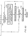
- FIG. 7 the block diagram of a possible physical configuration of a PCI network is shown. Each block in figure 7 is a PCI bridge or host bridge.
- host bridge A has three PCI bridges attached in a hierarchy behind it. Two of these PCI bridges, A1 and A2, are attached as peers to a PCI bus A, which is attached directly behind host bridge A. A PCI bridge B1 is then attached to a PCI bus B which is attached to the secondary side of bridge Al. Bridges B1 and A2 have PCI buses C and D, respectively, attached to their secondary sides.
- Host bridge B only has a PCI bus E attached to its secondary side.
- Host bridge C has a PCI bus F connected to its secondary side, which has a PCI bridge F1 attached to it.
- PCI bridge F1 then has a PCI bus G attached to its secondary side.
- Each of the bridges in figure 7 have two blocks in them with a number contained in each block.
- the top block represents the BUS_NO register of that particular bridge and the bottom block represents the SUB_BUS_NO register.
- the numbers in these blocks represent the values assigned to the registers by flow path 250 and subroutine 300 described in figures 5 and 6.
- flow path 250 is called by CPU 24 before any other configuration software for the system is activated.
- Flow path 250 begins by driving each bit of CONFIG_ENBL to a high individually.
- a specific bit in_CONFIG_ENBL will activate each of the host bridges A, B and C for a read cycle to their DEV_ATTR registers and the LSB of each of those registers will be counted by incrementing NO_HB in action step 264.
- Step 264 also generates the array of the bit numbers of CONFIG_ENBL that activate each bridge.
- NO_HB is equal to 3 or the number of host bridges in figure 7.
- action block 278 writes to CONFIG_ENBL a high signal at the bit number that activates host bridge A for internal configuration cycles. The first call to subroutine 300 is then made at block 282.
- Subroutine 300 begins by counting PCI bridges A1 and A2, by reading the DEV_ATTR registers of each device or PCI bridge attached to PCI bus A. This is accomplished by the loop procedure between blocks 306 and 314.
- NO_PB the value of NO_PB will be equal to two and the PB array will have been created.
- the PB array will indicate which bit numbers of the CONFIG_AD of host bridge A will activate PCI bridges A1 and A2 for a configuration cycle.
- Block 340 causes subroutine 300 to call itself. Accordingly, the counting and array creating procedure between blocks 306 and 314 is implemented to count the PCI bridges attached to PCI bus B. At the end of this procedure, NO_PB2 will be equal to 1, for PCI bridge B1, and the array of PB2 will have been created.
- the looping procedure between block numbers 324 and 332 then sets a temporary value for the SUB_BUS_NO of PCI bridge B1 and sets its BUS_NO to the permanent value of 2 in block 328.
- Block 340 then once again calls subroutine 300 for PCI bridge B1. This is the third layer of calls to subroutine 300.
- jj is equal to NO_PB at decision step 344 and subroutine 300 loops down to action block 352.
- BNO_MAX3, or 2 is copied into BNO_MAX2 at decision step 352 and a return is made at block 354 to the first layer of calls to subroutine 300.
- the value 2 is then copied into the SUB_BUS_NO register of bridge Al at block 342.
- the value 3 is copied into the BUS_NO of PCI bridge A2 at action block 346.
- subroutine 300 loops back up to block 336. Then, another second layer call to subroutine 300 is made for PCI bridge A2. This call returns to the first layer indicating that there are no PCI bridges attached to PCI bus D. Accordingly the BNO_MAX2 returned for that call is 3. This value is then copied into the SUB_BUS_NO of PCI bridge A2 at block 342.
- decision step 344 loops down to block 352 in which BNO_MAX is given the value of BNO_MAX2 or 3. Then a return is made to main flow path 250 at block 282.
- BNO_MIN is then set to equal 4 in block 288, and a loop is made back to block 276 to set the BUS_NO and SUB_BUS_NO registers of the remaining bridges.
- subroutine 300 First the value of 4 is copied into the BUS_NO of host bridge B. Then subroutine 300 is called, but it counts no PCI bridges on PCI bus E. Thus, it returns in block 320 with BNO_MAX equal to 4, and block 286 causes this value to be written into the SUB_BUS_NO of host bridge B.
- the ii value is not yet equal to NO_HB.
- decision step 290 causes a loop back to block 276.
- Block 284 writes 5 into the BUS_NO of host bridge C, then block 282 calls subroutine 300.
- Subroutine 300 must make a second layer call to find and count bus G.
- the BUS_NO and SUB_BUS_NO register of PCI bridge F1 are then set during the call to subroutine 300, and a BNO_MAX value of 6 is returned to block 282.
- ii is now equal to NO_HB meaning that all BUS_NO and SUB_BUS_NO registers have been set.
- block 292 sets all bit numbers of CONFIG_ENBL to high so that the configuration software can access the internal registers of the host bridges.
- the configuration software now has a preliminary map to locate all bridges, peripheral devices and buses in a multiple bus network.
Abstract

Description
- The present invention relates generally to information handling systems and more specifically to a method and apparatus for initializing multiple bus networks in an information handling system.
- Referring generally to information handling systems, they normally have as their main component a central processing unit (CPU), which directs all communications in the system and orchestrates all commands to be executed by the information handling system. Information handling systems also usually have a network, or networks, of physical connection devices called buses. These networks connect the CPU to any number of peripheral devices so that the CPU can communicate with the peripheral devices.
- In order for the CPU to communicate with a particular peripheral device in a multiple bus network, it must be able to locate the correct bus in the network to which the particular peripheral device is connected. Then the CPU must be able to locate the correct peripheral device on that bus with which it intends to communicate.
- Accordingly, a computer system that includes a network of multiple buses and peripheral devices must create an "address map" which indicates the location of each bus and peripheral device. The address map is normally created during the start-up or initialization phase of the system which is generally called configuration.
- During configuration, the CPU will access a software configuration program stored in the memory of the information handling system that will generate the address map. This configuration program will cause the CPU to access each peripheral device connected into the network to determine the amount of memory that each bridge and peripheral device requires in system memory and their location in the network. Then the CPU will reserve memory registers for each device and bus-to-bus bridge in the system's memory. After the memory locations are set for each device in memory, the configuration software causes the CPU again to access, and to "write" into, each peripheral device in the network the respective addresses of the registers in system memory that are reserved for it.
- During normal communication between the CPU and the multiple bus network, each peripheral device is able to communicate with the CPU by either decoding or encoding the addresses of the registers reserved for it in system memory. Accordingly, by assigning memory locations to each peripheral device in the network, the configuration software program creates the address map of the network that is used during normal communication.
- A problem exists with this method of creating the address map, however, because configuration software must be able to locate and access each bridge and peripheral device in the network before the address map is created. Thus, a "preliminary map" of the network must exist even before the address map can be created.
- One known method used to create this preliminary map is to use another software program that is written to generate the preliminary map for a specific physical configuration of the network. This program then generates the preliminary map each time the computer system is initialized upon start-up. To write such a program, the programmer must know the exact and entire hierarchical and peer configuration of the buses and peripheral devices that comprise the network.
- The problem with this method of creating the preliminary map is that it is inflexible. It is often desirable to change the physical configuration of the buses and devices that comprise the multiple bus network. For example, it may be desirable to add certain buses and peripheral devices to enhance the capabilities of the system.
- If the preliminary map is created through a program that is specific to one physical configuration of the network, however, each time the location of a bus is changed or a bus or device is removed from the system, the program must be rewritten. Furthermore, the programmer must have detailed knowledge regarding the changes in the physical system configuration and must know the exact location of each bus in the system. In sum, using a software program that is specifically written for a certain physical bus configuration to create the preliminary map is clumsy and time consuming should changes later be required in the physical configuration of the network.
- Another method for creating the preliminary map is to actually "hardwire" the preliminary map into each bus-to-bus bridge in the network. Bus-to-bus bridges are the hardware devices used to connect two buses together in the network. Thus, when the system is initialized on start-up the preliminary map of the entire network is already preset and fixed by default.
- Inflexibility is an even greater problem when this method is used. In a multiple bus network that uses a hardwired preliminary map, the hardware that provides the location of the bus-to-bus bridges and buses in the map would have to be replaced or "rewired" each time a change in the physical configuration of the network is required.
- Accordingly, a method and apparatus for initializing a multiple bus information handling system is needed that generates a preliminary map for buses in a multiple bus network that is not specific to any physical network configuration.
- A method and apparatus for initializing a multiple bus information handling system is further needed that will generate a new and different preliminary map for the multiple bus network should changes be implemented in the physical configuration of the system.
- Finally, a method and apparatus for initializing a multiple bus information handling system is further needed that does not require any additional hardware or that the preliminary map be hardwired into the network.
- Accordingly, the present invention provides a program that creates a preliminary map of a multiple bus network. This preliminary map is then used by configuration software of the information handling system to locate the peripheral devices in the multiple bus network to configure them. If the physical configuration of the multiple bus network should change in any way, the program can make corresponding changes in the preliminary map without having to rewrite or change the program.
- The invention will now be described, by way of example only, with reference to the accompanying drawings, in which:
- Figure 1 is a schematic drawing of an information handling system with multiple buses;
- Figure 2 is a block diagram of the configuration hardware of a bus-to-bus bridge;
- Figure 3 is a block diagram of a configuration cycle decode block in the bus-to-bus bridge of Figure 2;
- Figure 4 is a block diagram of the configuration hardware of a host bridge;
- Figure 5 is a flow chart of a software program used to provide a preliminary map of a multiple bus network.
- Figure 6 is a flow chart of a subroutine called by the software program of Figure 5;
- Figure 7 is a continuation of the flow chart of the subroutine of Figure 6; and
- Figure 8 is a block diagram of a typical PCI network.
- Referring now to Figure 1, a dual bus
information handling system 10 is shown generally at 10, comprising, (i) a processor, cache andmemory complex 12 connected to S-bus (system bus) devices 14 via an S-bus 16 and (ii) primary Peripheral Component Interconnect (PCI)devices 18 attached to one of the S-bus devices, a primaryPCI host bridge 20, via aprimary PCI bus 22. More detailed descriptions of the processor, cache andmemory complex 12, the S-bus devices 14, theprimary PCI devices 18, and the other elements shown in Figure 1 will be provided hereinafter. - The processor, cache and
memory complex 12 comprises a central processing unit (CPU) 24, a self-test circuit 26, amemory controller 28, aCPU cache 30, andbase system memory 32. TheCPU 24 in the preferred embodiment is a 32-bit microprocessor available from Intel, Inc. under the trade designation i486TM, although it is contemplated that thesystem 10 may be implemented using other types of CPUs, especially x86-type microprocessors. The self-test circuit 26 provides a built-in-self-test (BIST) feature for theCPU 24 upon power-up. The self-test circuit also controls any self-test features which may be provided within each of the S-bus devices 14. - The
CPU 24 is connected to the self-test circuit 26 and thememory controller 28 by a CPUlocal bus 34. Thememory controller 28 is connected to thebase system memory 32 by means of a basesystem memory bus 36. Thememory controller 28 controls read and write operations tobase system memory 32 over the basesystem memory bus 36, which operations are initiated by either theCPU 24 over the CPUlocal bus 34, or by an S-bus device 14 over the S-bus 16. Because the memory controller has the capability to manage operations on two buses, operations over the basesystem memory bus 36 and the CPUlocal bus 34 may be managed simultaneously. The CPUlocal bus 34, the basesystem memory bus 36, and the S-bus are 32-bit buses, each of which buses comprises data, address and control information paths as is typical of such buses. -
Base system memory 32 provides system-wide storage capability and may comprise either non-interleaved or interleaved memory cards. TheCPU cache 30 permits short term storage of information contained within eitherbase system memory 32 or expansion memory located elsewhere within thesystem 10. Such expansion memory could, for example, be located on the peripherally attached I/O devices within the system. TheCPU cache 30 incorporates random access memory (RAM) which is used to temporarily store address locations of thebase system memory 32 which are frequently accessed by theCPU 24. TheCPU 24 accesses information stored in theCPU cache 30 directly, whereas access to information stored in thebase system memory 32 must be handled by thememory controller 28. - All access to
base system memory 32 is controlled by thememory controller 28 via basesystem memory bus 36. The memory controller initiates system memory cycles to thebase system memory 32, during which cycles either theCPU 24 or one of the S-bus devices 14 has access to the base system memory via thememory controller 28. During a memory cycle, the memory controller does not pass information onto the S-bus. However, if the memory controller determines that the operation it is managing is an I/O cycle, the memory controller propagates the information onto the S-bus for access thereto by an S-bus device. If the I/O cycle is destined for a S-bus device, the appropriate S-bus device responds with a decode command to the memory controller. If the I/O operation is destined for aprimary PCI device 18, thePCI host bridge 20 responds with a decode command to the memory controller and passes the I/O cycle to the appropriate primary PCI device. - A
system clock module 38 provides a single clock signal for the S-bus devices 14, and a pair of clock signals for theCPU 24. In the preferred embodiment, the clock signal provided to the S-bus operates at 33 MHz. The two signals provided to theCPU 24 operate at 33 MHz and 66 MHz, respectively. TheCPU 24 requires two clock signals because it operates internally at 66 MHz, but communicates over the CPUlocal bus 34 at 33 MHz. - Communications between the processor, cache and
memory complex 12 and the S-bus devices are managed by thememory controller 28 over the 32-bit S-bus 16. Also attached to the S-bus, as shown in the preferred embodiment of Figure 1, are a direct memory access (DMA)controller 40, a system arbitration control point (SACP) 42, an input/output (I/O)controller 44, aPCMCIA controller 46, and apower management controller 48. An optionalpower management controller 50 may be attached to the power management controller 49 in case more sophisticated power management control is desired. Abuffer 52 is provided on the S-bus 16 intermediate theDMA controller 40 and the I/O controller 44. As shown in Figure 1, however, it is contemplated that other S-bus devices 14, beyond those shown, may be attached to the S-bus 16. - The
PCMCIA controller 46 is attached directly toPCMCIA card slots 54. Peripheral I/O devices 56 may be connected to thePCMCIA card slots 54 by means ofbuffers 58. The peripheral I/O devices 56 are controlled by the I/O controller 44. Attached to the I/O controller are a time-of-day clock 60 and aRAM module 62. The I/O controller 44 supports a variety of ports, including amouse port 64,serial ports 66, aparallel port 68, and akeyboard port 70. - In addition to supporting S-bus devices 14 on the S-
bus 16, thesystem 10 also supports a second high speed, high bandwidth bus, which in the preferred embodiment is theprimary PCI bus 22. ThePCI bus 22 is comprised of a new bus architecture called PCI. Theprimary PCI bus 22 is a high performance bus, meaning that it performs significant data transfer in a relatively short period of time, up to 120 megabytes of data per second. The PCI bus achieves this high level of performance, in part, because it may be directly linked to other high speed buses such as the S-bus 14, and thus may provide for a fast transfer of data between theCPU 24 or other S-bus devices 14 and theprimary PCI devices 18. In fact, the operation of several high integration devices, such as certain graphics packages, require a direct link to a system bus such as the S-bus through a high performance bus like thePCI bus 22. - In addition, the PCI bus architecture does not require any "glue logic" to operate peripheral devices connected to it. Glue logic for other buses typically consists of miscellaneous hardware components such as a decoders, buffers or latches that are installed intermediate the peripheral devices and the bus.
- The
primary PCI bus 22 operates on a synchronous clock signal of 33 MHz, and the strings of data transmitted over the PCI bus are 32 bits long. A 32-bit data string on the PCI bus is called a double word (DWORD), which is divided into 4 bytes each comprised of 8 bits of data. - The address and data information carried by the PCI bus are multiplexed onto one signal. Multiplexing eliminates the need for separate address and data lines, which in turn, reduces the amount of signals required in a PCI bus environment as opposed to other bus architectures. The number of signals required in PCI bus architecture is between 45-47 while standard non-multiplexed buses typically require twice this number. Accordingly, because the number of signals are reduced, the number of pins required to support a device linked to the PCI bus is also reduced a corresponding amount. PCI architecture is thus particularly adapted for highly integrated desktop computer systems.
- A more detailed description of the structure and operation of PCI bus architecture is provided in "Peripheral Component Interconnect (PCI) Revision 1.0 Specification", published June 22, 1992; "Preliminary PCI System Design Guide", revision 0.6, published November 1, 1992; "Peripheral Component Interconnect (PCI) Add-in Board/Connector Addendum", (Draft) published November 6, 1992; and, "Peripheral Component Interconnect (PCI) Revision 2.0 Specification," published April 30, 1993, all by the PCI Special Interest Group, the contents of which references are incorporated herein by reference as if they were fully set forth.
-
Primary PCI devices 18 in thesystem 10 communicate with each other over theprimary PCI bus 22. Primary PCI devices communicate with the CPU, cache andmemory complex 12 and with other S-bus devices 14 residing on the S-bus 16 by means of thePCI host bridge 20, which is itself an S-bus device residing on the S-bus. ThePCI host bridge 20, then, serves as an interface between the S-bus 16 and theprimary PCI bus 22 and provides an effective means of communication between these two buses, and any peripheral devices which may reside on these buses. - The
PCI host bridge 20 is a low latency interconnect mechanism through which theCPU 24 or other S-bus device 14 may directly access theprimary PCI devices 18 or devices attached thereto. Thebridge 20 also provides a high performance path which allows the primary PCI devices or devices attached thereto quick and direct access tobase system memory 32. In addition, thehost bridge 20 provides all of the hardware required to provide an interface between the S-bus 16 and theprimary PCI bus 22 so that data may be transferred between these buses. - The
primary PCI bus 22 is capable of supporting a variety of devices which are PCI compatible. As shown in Figure 1, these devices may include agraphics controller 72, a serial SCSI (small computer systems interface)controller 74, afuture PCMCIA controller 76, a standard bus (e.g., ISA or MICRO CHANNEL("MC-A"))
bridge 78, and a PCIsecondary bridge 80. The devices shown in Figure 1 attached to the primary PCI bus, however, are only one example of a system implementing a PCI bus architecture and thus the disclosed configuration and is not intended to limit the invention in any way. - The
graphics controller 72 is typically provided with memory capability in the form ofVRAM 82, which enables the graphics controller to buffer video frames therein, and may control any known graphics package which may be supported by PCI bus architecture. TheSCSI controller 74 serves as an interface betweenSCSI devices 84 attached to aSCSI bus 86 and theprimary PCI bus 22, and may control any SCSI device which may be supported by PCI bus architecture. Thefuture PCMCIA controller 76 is attached to andcontrols card slots 88. - The
standard bus bridge 78 serves as an interface between I/O devices 90 attached to a standard (e.g., MC-A or ISA)bus 92 and theprimary PCI bus 22. The architecture of an MC-A version of thestandard bus bridge 78 is the subject of the following copending patent applications assigned to the IBM Corporation: -
Secondary PCI devices 94 are connected toPCI bridge 80 viasecondary PCI bus 96. Any number of unidentifiedsecondary PCI devices 94 may be connected to thesecondary PCI bus 96. ThePCI bridge 80 serves as an interface between any number ofPCI devices 94 attached to thesecondary PCI bus 96 and theprimary PCI bus 22. - Any number of peripheral devices compatible with the PCI bus architecture may be arranged on the
primary PCI bus 22 with no other PCI buses present in theentire computer system 10; or any number of PCI peripheral devices could be attached to theprimary PCI bus 22 with any number of secondary PCI buses, in addition toPCI bus 96, attached through the same number of separate, respective PCI bridges 80 to theprimary PCI bus 22. Each secondary PCI bus could also have any number of additional PCI buses attached through PCI bridges to it and these "tertiary" PCI buses could have further PCI buses attached to them in various combinations. Similarly each PCI bus could have any number of PCI devices attached to it. Each connection between two PCI buses must be through a PCI bridge identical to bridge 80. - Furthermore, it is possible that a plurality of bridges identical to
PCI host bridge 20 could be driven by the S-bus 16. Each of these host bridges could then have any number of PCI buses, bridges and devices connected to them in any arrangement that the designer ofsystem 10 wishes. Thus, the portion ofsystem 10 that is comprised of PCI bus architecture may be comprised of multiple buses and PCI peripheral devices arranged in various peer and hierarchical combinations (referred to hereinafter generally as a PCI network). - In addition, an alternate configuration of
information handling system 10 eliminates S-bus 16 so thathost bridge 20 connectsprimary PCI bus 22 directly to CPUlocal bus 34. If there were any other PCI host bridges in the system, they would also be connected directly to CPUlocal bus 34. In this configuration, any of the S-bus devices 14 could be connected directly to CPUlocal bus 34. Since S-bus 16 and CPUlocal bus 34 operate using the identical bus architectures, the invention, as described below, functions the same in this alternate embodiment as it does in the preferred embodiment described in Figure 1. - A peer combination may be a group of buses or PCI devices at one level of PCI network. For example, the
graphics controller 72,standard bus bridge 78, andSCSI controller 74 are peers of each other. If there were several secondary PCI buses connected to theprimary PCI bus 22, rather than only one (80), they would all be peers. - The hierarchical combination of the PCI network is merely the layers of PCI buses that are all connected to the
primary PCI bus 22. For example, thesecondary PCI bus 96 is on the second level of the hierarchy of the PCI network or "behind" or "beneath"PCI bridge 80. - In the preferred embodiment of the invention, the multiple bus network of the computer system is a PCI network as shown in Figure 1 and described above. However, the invention described herein is not limited to PCI bus architecture, but is applicable to any multiple bus computer system in which a preliminary map of the bus network must be created before the system can be configured by the overall configuration software during initialization of the system.
- In PCI bus architecture, each PCI bridge and PCI peripheral device has a configuration space. This configuration space consists of 256 bytes of register space. The configuration space of each peripheral device and bridge contains the data used by the overall configuration software to create the address map to be used during normal communications. Accordingly, when the
CPU 24 runs the configuration software, it must access and read or write to the configuration space of each device or bridge to configure the system and create the address map. - Referring now to Figure 2, a function block diagram of the configuration hardware of
PCI bridge 80 is shown.PCI bridge 80 has two 32-bit registers called configuration address (CONFIG_AD) 150 and configuration data (CONFIG_DATA) (not shown), which are used specifically for configuration purposes.CONFIG_AD 150 is a latch, meaning that, once data is written into it, it will hold its contents until it receives a reset signal. - The
CONFIG_AD 150 and CONFIG_DATA are connected to theprimary PCI bus 22 throughinput line 156. The CPU transmits data over theprimary PCI bus 22 andline 156 intoCONFIG_AD 150 and CONFIG_DATA.CONFIG_AD 150 contains the location of the peripheral device or bridge theCPU 24 needs to configure based on the preliminary map and the location of the byte in that device's configuration space that must be accessed. - CONFIG_DATA contains the data that must be written into the device's or bridge's configuration space in the byte identified by
CONFIG_AD 150. If the CPU is accessing a particular device or bridge to read data from its configuration space, then CONFIG_DATA will receive the data contained in the specific byte identified byCONFIG_AD 150 to be read by theCPU 24. - The first two bits of
CONFIG_AD 150 are enable bits,bits numbers PCI bridge 80, which in the preferred embodiment isPCI bus 96. Thus, if the value of these bits is "01" then the PCI bridge runs a configuration cycle onPCI bus 96. - The remaining bits of
CONFIG_AD 150, except for bit numbers 24-31 which are unused, are divided into four specific fields. The first field is the BUS# field which is bit numbers 16-23 ofCONFIG_AD 150. The BUS# field identifies the bus in the PCI network to which the device to be accessed is connected. - The second field is the DEV# field, which is bit numbers 11-15. This field identifies the device to be accessed.
- The third field is the FUN# field, which is bit numbers 8-10. This field identifies an encoded value used to select 1 to 8 possible functions on the device specified by DEV#.
- The fourth and last field is the REG# field which is bit numbers 2-7. This field identifies the register to be accessed in the configuration space of the device targeted by the configuration cycle.
- The
CONFIG_AD 150 is connected to a configuration cycle decode block (CONFIG BLOCK) 152 through a plurality ofinput lines 154 a-f.CONFIG_AD 150 also is connected to theprimary PCI bus 22 throughline 156.CONFIG BLOCK 152 is also connected to theprimary PCI bus 22 by aninput line 157, labeled IDSEL. -
Line 156 also connects three other registers in thePCI bridge 80 to theprimary PCI bus 22; a device attribute register (DEV_ATTR) 158, a bus number register (BUS_NO) 160 and a sub-bus number register (SUB_BUS_NO) 162. TheDEV_ATTR 158, BUS_NO 160 andSUB_BUS_NO 162 are also connected toCONFIG BLOCK 152 throughlines 164, 166 and 168, respectively. -
DEV_ATTR 158 may be at least one bit in length since its least significant bit (LSB) is the only bit used in configuration. The sole purpose of theDEV_ATTR 158 is to indicate whether the apparatus theDEV_ATTR 158 is contained in is a PCI bridge or a peripheral device. The LSB ofDEV_ATTR 158 is always set to a 1 to indicate thatPCI bridge 80 is, in fact, a PCI bridge. IfDEV_ATTR 158 was in a peripheral device, it would always be set to 0. - BUS_NO 160 is 8 bits in length. The BUS_NO 160 contains an identification number for the bus directly behind
PCI bridge 80, in this case,secondary PCI bus 96. -
SUB_BUS_NO 162 is also 8 bits in length. TheSUB_BUS_NO 162 contains an identification number of the bus with the highest identification number behindbridge 80, which is once againsecondary PCI bus 96 since there are no other buses behindPCI bridge 80. - The identification numbers stored in BUS_NO 160 and
SUB_BUS_NO 162 provide the preliminary map required for initialization of the PCI network explained above. The inventive method used to obtain these identification numbers is set forth in detail below. -
PCI bridge 80 also has two other function blocks; a PCI bus address decode block (DECODE BLOCK) 170 and a PCI bus cycle translation block (TRANS BLOCK) 172.DECODE BLOCK 170 andTRANS BLOCK 172 are connected to thePrimary PCI bus 22 through line 174.TRANS BLOCK 172 is also connected to theprimary PCI bus 22 throughline 156. -
DECODE BLOCK 170 is connected to theCONFIG BLOCK 152 throughoutput lines DECODE BLOCK 170 is also connected to CONFIG_AD 150 through anoutput line 180. -
TRANS BLOCK 172 is connected to theCONFIG BLOCK 152 by an internal cycle line (INT_CYC) 182 and an external cycle line (EXT_CYC) 184.TRANS BLOCK 172 also receives input fromCONFIG BLOCK 152 through aninput line 186.TRANS BLOCK 172 is also connected tosecondary PCI bus 96 through anoutput line 188. - The function of
DECODE BLOCK 170 is to receive control signals from theCPU 24 throughPCI bus 22 and line 174 and to translate them into a read or write enable signal to be sent to theCONFIG BLOCK 152 orCONFIG_AD 150. Enable signals to theCONFIG BLOCK 152 are generated on CFG_RD and CFG_WR and designate whether a particular configuration cycle will be a read or a write operation, respectively. In other words, ifDECODE BLOCK 170 generates an enable signal on CFG_RD, then the present configuration cycle is a read operation. WhenDECODE BLOCK 170 enablesline 180, it allows theCPU 24 to read or write intoCONFIG_AD 150 throughline 156 to begin a configuration cycle. - The
CONFIG BLOCK 152 is the center of all configuration operations inPCI bridge 80. One function ofCONFIG BLOCK 152 is to receive the contents ofCONFIG_AD 150 through the plurality oflines 154 a-f, receive the contents of BUS_NO 160 andSUB_BUS_NO 162, and compare the BUS# field ofCONFIG_ADD 150 with the contents of BUS_NO 160 andSUB_BUS_NO 162. Then, based on this comparison and other information received fromIDSEL 157,CONFIG BLOCK 152 determines whether the present configuration cycle is intended for a peripheral device attached tosecondary PCI bus 96, a device attached to another bus in the PCI network that is located somewhere behind PCI bridge 80 (of course, however, the embodiment shown in figures 1 and 2 has no other PCI bridges), or thePCI bridge 80 itself. - If the configuration cycle is intended for any bus behind
PCI bridge 80,CONFIG BLOCK 152 decodes the contents ofCONFIG_AD 150 and transfers it toTRANS BLOCK 172.CONFIG BLOCK 152 will also send an enable signal toTRANS BLOCK 172 onEXT_CYC 184 if the present configuration cycle is targeted for a device linked to a bus behindPCI bridge 80. - If the configuration cycle is intended for the
PCI bridge 80 itself,CONFIG BLOCK 152 will decode the REG# field to identify a register in its own configuration space and perform a read or write operation with respect to this internal register. If the configuration cycle is an internal one,CONFIG BLOCK 152 will also send an enable signal toTRANS BLOCK 172 onINT_CYC 182. -
TRANS BLOCK 172 performs all of the timing and signal translation betweenprimary PCI bus 22 andsecondary PCI bus 96 so that signals may be passed back and forth between them. This translation is the primary function ofPCI bridge 80 and is beyond the scope of the invention described herein. - With respect to configuration cycles, the only functions of
TRANS BLOCK 172 is to transmit the decoded contents ofCONFIG_AD 150 fromCONFIG BLOCK 152 ontosecondary PCI bus 96.TRANS BLOCK 172 will only perform this function when it receives an enable signal onEXT_CYC 184 fromCONFIG BLOCK 152. - Referring now to Figure 3, a block diagram of
CONFIG BLOCK 152 is shown.CONFIG BLOCK 152 includes acomparator 190, afirst logic block 192, asecond logic block 194 and adecoder 196, which are all connected by various signal lines as shown in Figure 3.Logic block 192 includes adecoder 198 and an and gate (AND1). - The BUS# field of
CONFIG_AD 150 is connected by line 154a tocomparator 190 anddecoder 196. The REG# field ofCONFIG_AD 150 is connected byline 154d todecoders CONFIG_AD 150 is connected tologic block 194 anddecoder 196 byline 154b. The FUN# field ofCONFIG_AD 150 is connected to decoder 196 by line 154c. - Other inputs to
CONFIG BLOCK 152 includeIDSEL 157 andbit numbers CONFIG_AD 150 which are attached to AND1 oflogic block 192.CFG_RD 176 andCFG_WR 178 are also both attached as inputs tologic blocks SUB_BUS_NO 162 are both connected as separate inputs tocomparator 190 throughlines 166 and 168, respectively. - The output lines from
logic block 192 areINT_CYC 182, afirst output line 200 fromdecoder 198 and asecond output line 202. As set forth below, these are all used to perform configuration cycles directed to internal registers ofPCI bridge 80. -
EXT_CYC 184 is the only output fromlogic block 194.Line 186 attaches the output ofdecoder 196 toTRANS BLOCK 172.Comparator 190 has twooutput lines - In operation, when a configuration cycle is asserted by
CPU 24 onprimary PCI bus 22,PCI bridge 80 will interpret it as targeted for one of three destinations: a register within the configuration space of the PCI bridge itself; a register within the configuration space of a peripheral device or another PCI bridge attached to thesecondary PCI bus 96; or a register within the configuration space of a peripheral device or PCI bridge attached to a PCI bus belowsecondary PCI bus 96 in the hierarchy of the PCI network. - To start a configuration cycle on the
primary PCI bus 22, theCPU 24 sends control signals throughprimary PCI bus 22 to theDECODE BLOCK 170, which causesDECODE BLOCK 170 to send a write signal to CONFIG_AD 150 online 180. This allows the CPU to write a configuration address intoCONFIG_AD 150 and this address is latched there untilCONFIG_AD 150 is reset byDECODE BLOCK 170. The contents ofCONFIG_AD 150 is then accessed byCONFIG BLOCK 152 through plurality of lines 154a-f. - When the configuration cycle is directed to an internal register of the
PCI bridge 80, the value ofbit numbers CONFIG_AD 150 are set to "00". In addition, an enable signal is sent by theCPU 24 through thePCI host bridge 20 to theCONFIG BLOCK 152 onIDSEL 157. - The enable signal on
IDSEL 157 and the "00" signal frombit numbers CONFIG_AD 150 are input to AND1 oflogic block 192 which together generate an enabling high signal on the output of AND1. This signal energizesdecoder 198 to decode the REG# field ofCONFIG_AD 150.Decoder 198 then generates an output online 200 which accesses the internal configuration register ofPCI bridge 80 that corresponds to REG#. - Simultaneously,
DECODE BLOCK 170 generates an enable signal on eitherCFG_RD 176 orCFG_WR 178, depending on whether a read or write operation, respectively, is to be executed during this particular configuration cycle.Logic block 192 passes the read or write command out online 202 and a read or write operation is conducted on the internal register accessed by the decoder output online 200.Logic block 192 also enablesINT_CYC 182, which signals toTRANS BLOCK 172 that the configuration cycle is directed to the PCI bridge internally and no information is to be transmitted ontosecondary PCI bus 96. - When the configuration cycle is not directed to the internal configuration space of
PCI bridge 80, IDSEL is not enabled andbit numbers CONFIG_AD 150 have the value "01" as set byCPU 24 throughPCI host bridge 20. Thus, these signals do not enable AND1 anddecoder 198, and therefore,INT_CYC 182 is not activated and no internal configuration occurs. - Instead, after the configuration address is latched into
CONFIG_AD 150,comparator 190 receives the BUS# field ofCONFIG_AD 150 as an input through line 154a. At the same time,comparator 190 also receives the contents of BUS_NO 160 andSUB_BUS_NO 162 as inputs fromlines 166 and 168, respectively. -
Comparator 190 then compares the value of BUS# with the values of BUS_NO 160 andSUB_BUS_NO 162. If BUS_NO 160 is equal to BUS#, then the present configuration cycle is intended for a peripheral device or another PCI bridge attached to thesecondary PCI bus 96, andline 204 is enabled bycomparator 190, which activatesdecoder 196 andlogic block 194. - When
decoder 196 is activated, it decodes the DEV# field ofCONFIG_AD 150 into a 21-bit value. Each bit number of the decoded 21-bit value may be attached to an the enable line (IDSEL) of a device or PCI bridge onsecondary PCI bus 96. Thus, in the preferred embodiment, a maximum of 21 peripheral devices or PCI bridges can be attached to thesecondary PCI bus 96, or any other PCI bus in the PCI network. - Only one of these bits will be set to an enabling high, or the value "1", with the rest being set to low, or "0". Thus, the decoded 21-bit value of DEV# will enable only the device on
secondary PCI bridge 96 that is the target of the configuration cycle. - The decoder, when activated, also drives the value of
bit numbers CONFIG_AD 150 to "00". This signals to the devices and PCI bridges attached tosecondary PCI bus 96 that the present configuration cycle is targeted for one of them. - The
decoder 196 simply passes on the values of FUN# and REG# toTRANS BLOCK 172 to be sent ontosecondary PCI bus 96. - If the value of BUS# is greater than the value of BUS_NO 160, but less than or equal to SUB_BUS_NO 162, then the present configuration cycle is intended for a peripheral device or PCI bridge attached to a PCI bus that is lower in the hierarchy of the PCI network than
secondary PCI bus 96. In this situation,comparator 190 will enableline 206 which enableslogic block 194. - Additionally, when this particular situation occurs,
decoder 196 is not activated. Thus, it simply passes the present values of all of the fields ofCONFIG_AD 150, including the "01" value ofbit number TRANS BLOCK 172. - When
logic block 194 is activated bylines EXT_CYC 184, which signals toTRANS BLOCK 172 that the present configuration cycle is targeted to a device or PCI bridge external toPCI bridge 80. Accordingly,TRANS BLOCK 172 will transfer the values of the fields ofCONFIG_AD 150 it receives online 186 fromCONFIG BLOCK 152 out ontosecondary PCI bus 96. - If the configuration cycle is targeted for a device or PCI bridge on
secondary PCI bus 96, the decoded value of DEV# enables the appropriate device or bridge and, becausebit numbers secondary PCI bus 96 fromCPU 24 will determine whether the configuration cycle is a read or write operation. - If the configuration cycle is targeted for a device or PCI bridge that is connected to a PCI bus beneath
bus 96 in the hierarchy of the PCI network, then CONFIG_AD 150 is simply passed along to the PCI bridges behindbus 96, which will each perform the BUS# comparison procedure described above until a bridge is located that has a BUS_NO equal to BUS#. Then this particular PCI bridge will decode the DEV# and the configuration cycle will be performed in the configuration space of the targeted device attached to the bus on the secondary side of that bridge. - Thus, the hardware of each PCI bridge in a PCI network is standardized and does not change from bridge to bridge. In addition, the hardwired logic that comprises each bridge is known.
- Referring now to Figure 4, a block diagram of the hardware used for configuration of
host bridge 20 is shown. As Figure 4 illustrates, the configuration hardware ofhost bridge 20 is substantially similar to the configuration hardware ofPCI bridge 80, depicted in Figure 2. Indeed,host bridge 20 has aDECODE BLOCK 208, aCONFIG BLOCK 210, and aTRANS BLOCK 212. It also has the following registers: aCONFIG_AD register 214, aDEV_ATTR register 216, aBUS_NO register 218 and aSUB_BUS_NO register 220. The function of these components ofhost bridge 20 are substantially the same as their respective counterparts inPCI bridge 80. - The only hardware differences between
host bridge 20 andPCI bridge 80, are thathost bridge 20 includes some additional hardware to accommodate aninformation handling system 10 that has a plurality of host bridges and PCI networks. This additional hardware includes a configuration enable register (CONFIG_ENBL) 222, which is connected by enable output (ENBL_OUT) 224 to s-bus 16. Anadditional output line 226 runs fromDECODE BLOCK 208 to CONFIG_ENBL 222 to provide read and write signals to CONFIG_ENBL 222. An andgate 228 is also provided with an input from the most significant bit ofCONFIG_AD 214 and another input from s-bus 16 calledEXT_ENBL 232. Andgate 228 also has an output line 234. -
CONFIG BLOCK 210 also has one small difference when compared toCONFIG BLOCK 152. The AND1 gate of CONFIG BLOCK 210 (not shown) receives two of its inputs from DEV# and the comparator ofCONFIG BLOCK 210 instead of frombit numbers CONFIG BLOCK 152. Accordingly, the AND1 ofCONFIG BLOCK 210 only allows a configuration cycle to the internal registers ofhost bridge 20 when BUS# and DEV# are equal to 0. If DEV# is greater than 0 and BUS# is equal to 0, then the configuration cycle is directed byCONFIG BLOCK 210 to a device attached to the PCI bus connected to the secondary side of the host bridge. - The
CONFIG_ENBL 222 is a 32-bit register that has, in a multiple host bridge system, each individual bit attached to theEXT_ENBL 232 of a different host bridge. Accordingly, when a configuration cycle is directed to the internal registers of a particular host bridge, only one bit of CONFIG_ENBL will be high and that bit will be attached to the EXT_ENBL of the host bridge to which the configuration cycle is directed. - In operation, the
CPU 24 will causeDECODE BLOCK 208 to generate a write command online 226 to CONFIG_ENBL 222 and a value provided byCPU 24 on s-bus 16 will be written intoCONFIG_ENBL 222. This 32-bit value will have only one bit high and the rest low. - The
CPU 24 will then causeDECODE BLOCK 208 to send a signal online 226 that causesCONFIG_ENBL 222 to transmit the 32-bit value onto s-bus 16 through ENBL_OUT 224. Then the host bridge that has its EXT_ENBL connected to the bit in the 32-bit signal having a high value will be activated for the present configuration cycle. - Assuming that
EXT_ENBL 232 is activated by the high bit number in ENBL_OUT 224, if the most significant bit ofCONFIG_AD 214 is high as set by theCPU 24, then andgate 228 will generate an enable signal on line 234. This will causeCONFIG BLOCK 210 to perform a configuration cycle on the internal registers ofhost bridge 20, assuming that both DEV# and BUS# are equal to 0. If the bit number of CONFIG_ENBL 222 that is set to a high, is attached to the EXT_ENBL of a different host bridge, then that particular bridge will be activated for an internal configuration cycle. - All of the PCI host bridges in an information handling system may be comprised of the same hardware. Only one of the host bridges, however, needs to have a CONFIG_ENBL register. Thus, to preserve the standardization of host bridges in a system, each bridge may be manufactured with a CONFIG_ENBL register, but the register would only be connected and used in one host bridge per system. Also, the CONFIG_ENBL register could be external to the host bridges if desired.
- Accordingly, as the above explanation of configuration space access indicates, the preliminary map that is used in the preferred embodiment to access the configuration spaces of the various bridges and devices that comprise the PCI network are the values of BUS_NO and SUB_BUS_NO. Previously, no method or apparatus existed that would provide the correct values for BUS_NO and SUB_BUS_NO, when the physical configuration of the PCI network changed, without reprogramming the configuration software of the entire system. The inventive software program described below, however, will provide correct values for BUS_NO and SUB_BUS_NO for each bridge in the PCI network without any reprogramming, even if the physical configuration of the PCI network changes dramatically between shut-down and start-up of
system 10. - This program is stored in
system memory 32 and is accessed and run byCPU 24 during configuration of the system, before any other configuration cycles begin to run. The program causes several read and write cycles to be executed on the internal configuration registers, BUS_NO and SUB_BUS_NO, of the PCI bridges and host bridges in the system. - The program can be divided into two main decision and action paths (flow paths). The first flow path is the main flow path of the program and is shown in Figure 5. This main flow path has the capability to map the bus numbers and sub-bus numbers of information handling systems that have a plurality of host bridges, and thus, a plurality of PCI networks.
- The second flow path is for a subroutine that is called by the main flow path for each host bridge and which is then called repeatedly by itself for each bus in the PCI network. Accordingly, since the subroutine calls itself repeatedly, it is referred to herein as a "recursive" subroutine. Figure 6 depicts the recursive subroutine. The main functions of the recursive subroutine are to count the PCI bridges attached to each bus, to set temporary values for the BUS_NO and SUB_BUS_NO of each PCI bridge as it moves down through the levels of the hierarchy that comprise a PCI network by recalling itself for each PCI bus, and to set permanent values for the BUS_NO and SUB_BUS_NO of each PCI bridge once the subroutine returns from a call to it for a bus attached to a particular bridge.
- Referring now specifically to figure 5, a main flow path of a
preliminary mapping program 250 is shown. Two pointers or counters are referred to throughout the flow path. These pointers are indicated by the variables i and ii. A constant, HB_MAX, is also used, which indicates the maximum number of host bridges that may be present in a computer system. HB_MAX is set by the limitations of theCPU 24 or the system designer. Flowpath 250 uses a memory array HB for recording the bit numbers of CONFIG_ENBL assigned to each bridge. For example, HB(1) records the bit number of CONFIG_ENBL that will enable host bridge No. 1, the first host bridge in the system. - The
main flow path 250 has astart 252 which begins the program when it is called by theCPU 24 upon start-up or initialization of the system. The BUS_NO values of all host bridges are set to 00 as a default upon start-up of the computer system. Start 252 then proceeds to anaction step 254 in which the pointer i and a variable NO_HB are set to 0. The variable NO_HB is the number of host bridges in the system as they are counted byflow path 250. - Flow
path 250 then proceeds to anaction step 256 in which a 32-bit value is written into the CONFIG_ENBL register having only one bit number that is high, and this bit number is identified by the pointer i. Thus, for example, in the first iteration offlow path 250,bit number 0 of CONFIG_ENBL will be high and the rest of the bits of this register will be low. Then, i is incremented in anaction step 258. - The next step in
flow path 250 is anaction step 260 which conducts a read configuration cycle to a DEV_ATTR register with the fields ofCONFIG_AD 214 set to BUS#=0, DEV#=0. Continuing with the example set forth immediately above, if the EXT_ENBL input of a host bridge is attached to bitnumber 0 ofCONFIG_ENBL 222,action step 260 will cause the CPU to read the contents of the DEV_ATTR register of that host bridge. This is because all host bridges respond to a configuration cycle when the values of BUS# and DEV# are equal to 0. The only way to enable the host bridges individually for a configuration cycle is by their different EXT_ENBL inputs fromCONFIG_ENBL 222. -
Decision step 262 is the next step inflow path 250.Decision step 262 evaluates whether the least significant bit of the DEV_ATTR register has a high value. If this is true, then a host bridge is attached to bitnumber 0 of theCONFIG_ENBL 222 anddecision step 262 transfers to anaction step 264 in which NO_HB is incremented by one to count the number of host bridges in the system and the bit number of CONFIG_ENBL 222 which activated the host bridge,bit number 0, is stored in the memory array with the variable set to HB(i) or HB(1). - If no host bridge is attached to bit
number 0 then no device responds to the configuration read cycle, and thus, the CPU judges the LSB of the DEV_ATTR register of the non-responding host bridge to be 0. Accordingly, NO_HB is not incremented and no host bus is counted. - After
decision step 262 andaction step 264,flow path 250 goes to another decision step 266, which compares i with HB_MAX. If i is less than HB_MAX, then flowpath 250 loops back to action step 256 which writes a new value to CONFIG_ENBL 222 having the next bit number, equal to an incremented i, high and the other bit numbers equal to 0. This looping continues until i is equal to HB_MAX meaning that all host bridges that could possibly be ininformation handling system 10 have been located and counted. Accordingly, NO_HB will equal the total number of host bridges in the system and the HB array will indicate the values of CONFIG_ENBL that must be generated hy theCPU 24 to access each host bridge's configuration space. When this is true, then decision step 266 goes onto anotherdecision step 268. - At
decision step 268, NO_HB is compared with 0. If NO_HB is equal to 0, then theCPU 24 judges at anaction block 270 that there are no host bridges ininformation handling system 10, and thus, that a preliminary map of BUS_NO and SUB_BUS_NO registers is not required for configuration. Accordingly, the program stops at anend 272. - If NO_HB is greater than 0, then there is at least one host bridge in the computer system and at least one PCI network for which a preliminary map of BUS_NO and SUB_BUS_NO must be generated. Accordingly, the
flow path 250 will continue fromdecision step 268 to anaction step 274. -
Action step 274 introduces two new variables to flowpath 250, BNO_MIN and BNO_MAXTMP. BNO_MIN is the minimum value for BUS_NO that increases throughflow path 250 as the number of buses located in the PCI network increase. BNO_MAXTMP is the temporary value that flowpath 250 sets for the SUB_BUS_NO of each PCI bridge which decreases as the number of buses located in the PCI network increases.Action step 274 sets the initial values of pointer ii to 0, BNO_MIN to 00 and BNO_MAXTMP to FF hexadecimal. - Flow
path 250 moves on to anaction step 276 which increments pointer ii by one and then moves on to anotheraction step 278. A write configuration cycle is performed to the CONFIG_ENBL register 222 byaction step 278. The value written to CONFIG_ENBL 222 in this step is from the HB(NO_HB) array with (NO_HB) having the value of ii. Thus, if the value of ii is 1, the array value for host bridge NO. 1, which is the value that will enable theEXT_ENBL 232 of host bridge NO. 1, is written intoCONFIG_ENBL 222. This will allow configuration read and write cycles to be performed to the internal registers of host bridge NO. 1 asflow path 250 progresses, specifically the BUS_NO and SUB_BUS_NO registers of host bridge NO. 1. - A
decision step 280 is the next step inflow path 250.Decision step 280 determines whether ii is greater than 1, and if not, then it loops to acall block 282 skipping anaction block 284. Callblock 282 calls arecursive subroutine 300, which is shown in Figure 6. Thus, for the first call ofsubroutine 300, when ii is equal to 1, meaning that the preliminary map for the PCI network behind the first host bridge in the computer system is being generated,flow path 250 skipsaction block 284. - For the purpose of
understanding flow path 250, only the value of BNO_MAX returned to flowpath 250 by the call ofsubroutine 300 need be discussed. If the BUS_NO register of the host bridge that corresponds to ii has the value x and the total number of PCI buses in the PCI network behind that host bridge is z, then the value for BNO_MAX returned bysubroutine 300 is x + z - 1. The method by whichsubroutine 300 derives this value is discussed in detail below. - Therefore, assuming that this is the first call of
subroutine 300 for the first host bridge in the computer system, BNO_MIN equals 0 by default; and assuming, for example there are a total of 4 PCI buses in the PCI network behind the first host bridge, the value returned bysubroutine 300 for BNO_MAX will be 3. This means that the BUS_NO register of the host bridge and the bus immediately behind it were assigned the value of 0 (which the host bridge had as a default value), and the BUS_NO registers of the 3 PCI bridges behind that host bridge and the PCI buses behind them were assigned thevalues 1 through 3, respectively, bysubroutine 300. - After
call block 282 returns with the value for BNO_MAX, flow path goes onto anaction step 286 in which a configuration write cycle is conducted to the SUB_BUS_NO register of the present host bridge as indicated by ii. The value written into the SUB_BUS_NO is BNO_MAX. - Accordingly, continuing with the example discussed in the immediately preceding paragraph, the
value 3 will be written into the SUB_BUS_NO of the first host bridge in the system. Thus, the values of the BUS_NO and SUB_BUS_NO registers for the first host bridge in the system will be 0 and 3, respectively. The host bridge will now only respond to configuration cycles in which the BUS# field is equal to 0 through 3, which are the identification numbers assigned to the respective PCI buses in the PCI network behind the host bridge. - The next step in
flow path 250 is anaction step 288 which derives a new value for BNO_MIN by adding 1 to BNO_MAX. This new BNO_MIN will be the BUS_NO of the next host bridge in the computer system, if one exists, and the number assigned to the bus immediately behind that host bridge. - The next step in
flow path 250, adecision step 290, performs the function of determining whether there are any more host bridges in the system by comparing ii to NO_HB. If NO_HB exceeds ii then, there are more host bridges in the system and decision step 290 loops back to action block 276 in which ii is incremented. If this occurs, then BNO_MIN is written into the BUS_NO register of the next host bridge in the system byaction block 284. Thensubroutine 300 is called and the whole procedure repeats itself. - The procedure repeats for each host bridge until ii is equal to NO_HB, then
decision step 290 proceeds toaction step 292, in which all bits ofCONFIG_ENBL 222 are set to high for the remainder of the configuration procedures to be performed by the configuration software of the computer system. This allows the configuration software to access the configuration spaces of all host bridges if needed. - The program then ends at
block 294. At this time, a complete preliminary map of all PCI networks in the system will have been created based on the BUS_NO and SUB_BUS_NO registers of all bridges in the system. If the physical configuration of the PCI networks should change, the preliminary map can be changed simply by re-initializing the computer system without any reprogramming. - Referring specifically now to figure 6, the flow path of
subroutine 300 is shown.Subroutine 300 has two pointers, j and jj. DEV_MAX is a constant used bysubroutine 300, which is the maximum number of peripheral devices or PCI bridges that can be connected to one PCI bus. As set forth above, the DEV_MAX of the preferred embodiment is twenty-one (21). -
Subroutine 300 also uses several variables, including BNO_MIN, BNO_MAXTMP, and BNO_MAX. As set forth above, the values for BNO_MIN and BNO_MAXTMP are set by themain flow path 250 before it callssubroutine 300. The initial values of these variables, as set forth above, are 00 and FF, respectively. BNO_MAX is the variable that subroutine 300 returns to flowpath 250. - Another variable used by
subroutine 300 is NO_PB. NO_PB is the number of PCI bridges connected to a particular PCI bus. - When it is called by
flow path 250,subroutine 300 begins atstart 302 and proceeds toaction step 304 in which NO_PB and j are set to 0.Subroutine 300 then proceeds toaction step 306 in which j is incremented by 1. -
Subroutine 300 then begins its first main procedure which is to count the PCI bridges attached to the bus for which the subroutine was called. The steps that accomplish this task areaction steps -
Action step 308 begins by performing a configuration read cycle to DEV_ATTR with BUS# equal to BNO_MIN and the DEV# field equal to j, which on the first iteration of the counting procedure is 1.Decision step 312 then determines if the LSB of DEV_ATTR is a 0 or 1. If the LSB is all, then the device responding to the read is a PCI bridge, and thesubroutine 300 branches off to action step 310 which increments NO_PB to count the number of PCI bridges attached to the PCI bus and creates a PB array by inserting j into the value for PB(NO_PB). This array when completed will indicate the various DEV# values that will activate each PCI bridge to access their internal configuration spaces. This array is similar to the HB array inflow path 250. - If the LSB of DEV_ATTR is a 0, this means that there is a device that is activated by the DEV# having the value j, but it is a regular PCI device and not a PCI bridge. In this case, the
CPU 24 notes that a device is activated by that particular DEV#, but does not increment NO_PB. Instead the subroutine proceeds todecision step 314. If there is no peripheral device or PCI bridge that is activated by DEV# equal to j, theCPU 24 also notes this information and proceeds todecision step 314. -
Decision step 314 compares j with DEV_MAX. If j is less than DEV_MAX, then subroutine 300 loops back toaction step 306 in which j is incremented. Accordingly, this loop will repeat until the value of j is equal to DEV_MAX. - When this occurs, NO_PB will be equal to the number of PCI bridges attached to the particular PCI bus for which the call to subroutine 300 was initiated (the calling PCI bus). Also, the PB array will be complete, and a chart will have been created in
system memory 32 byCPU 24 that is similar to the following:BUS# DEV# Device 0 0 HOST Bridge 0 1 PCI Device 0 2 (nothing) 0 3 PCI Bridge 0 4 PCI Bridge : : : : : : 0 21 : - Subroutine then proceeds to a
decision step 316 which determines if there are any PCI bridges attached to the calling PCI bus. NO_PB is compared to 0 indecision step 316 and, if NO_PB is equal to 0, then there are no PCI bridges. If this is the case, then subroutine 300 goes to action step 318 which transfers the value of BNO_MIN into BNO_MAX.Subroutine 300 then returns to themain flow path 250 in areturn block 320. If NO_PB is greater than 0, then at least one PCI bridge is connected to the calling PCI bus, andsubroutine 300 proceeds fromdecision step 316 to anaction step 322. -
Action step 322 is the beginning of a looping sequence insubroutine 300 in which temporary values are set in the BUS_NO and SUB_BUS_NO registers of the PCI bridges attached to the calling bus.Action step 322 sets jj to 0 and then proceeds to anaction step 324, which increments jj by 1. - The next step in
subroutine 300 is adecision step 326, in which a determination is made whether jj is equal to 1. If jj is indeed 1, then this is the first iteration through this looping sequence, and thesubroutine 300 proceeds toaction step 328.Action step 328 performs a write configuration cycle with BUS# = BNO_MIN, DEV# = PB(jj), and REG# = BUS_NO. The value written in this configuration cycle isBNO_MIN + 1. The result of this write configuration cycle is that the BUS_NO value of the first PCI bridge attached to the calling bus is set atBNO_MIN + 1. For example, if this is the first call ofsubroutine 300 for a bus directly behind a PCI host bridge, this BUS_NO value will be 1.Subroutine 300 then proceeds to anaction step 330. - If
decision step 326 determines that jj is not equal to one, then this is not the first iteration through the looping procedure anddecision step 326 proceeds to an action step 333. Action step 333 causes a write to the BUS_NO address of a PCI bridge on the calling bus with DEV# = PB(jj). The value written into the BUS_NO is BNO_MAXTMP - NO_PB + jj. This value is a temporary value for BUS_NO while thesubroutine 300 moves down through the PCI network to the bottom level of the PCI hierarchy. Action step 333 then goes toaction step 330. -
Action step 330 performs a configuration write cycle to a SUB_BUS_NO of the PCI bridge attached to the calling bus that responds when DEV# = PB(jj). The value written into SUB_BUS_NO is a temporary value equal to BNO_MAXTMP - NO_PB + jj. -
Subroutine 300 then proceeds to adecision step 332, which causes thesubroutine 300 to loop back toaction step 324 until jj is equal to NO_PB. When this is true then a table of temporary values for each PCI bridge will have been created similar to the table shown below:
- The PCI buses attached to the secondary sides of the bridges in this table represent the second layer of the hierarchy of the PCI network. The PCI buses attached to the host bridges in the system represent the first layer of the hierarchy.
-
Subroutine 300 then moves toaction step 334, which begins the recursive portion of the subroutine.Action step 334 sets counter jj to 0 and sets the value of a new variable, BNO_MIN2, toBNO_MIN + 1. - The next step is an
action step 336 in which jj is incremented by 1.Action step 336 is followed by another action step 338 in which a new variable, BNO_MAXTMP2, is introduced. Action step 338 gives BNO_MAXTMP2 the value of BNO_MAXTMP - NO_PB + jj. -
Subroutine 300 then moves on to acall block 340 in which subroutine 300 calls itself to count the PCI bridges attached to the second layer of PCI buses in the PCI hierarchy. The number of PCI bridges attached to this second layer of buses will indicate the number of PCI buses in the third layer of the PCI hierarchy. - During this second call of
subroutine 300 atcall block 340, the variables used in place of BNO_MIN and BNO_MAXTMP are BNO_MIN2 and BNO_MAXTMP2, respectively. Similarly, the return value from this second call will be a variable BNO_MAX2 instead of BNO_MAX. If x equals the number of PCI bridges, and thus, PCI buses behind the PCI bridge identified as PB(jj), then the return value of BNO_MAX2 will be BNO_MIN2 + x - 1. BNO_MAX2 is the reference number of the PCI bus with the highest reference number behind the particular PCI bus, PB(jj). - When
call block 340 returns a value for BNO_MAX2,subroutine 300 moves on to anaction block 342.Action block 342 causes a configuration write cycle to be executed to a SUB_BUS_NO register with BUS# = BNO_MIN, DEV# = PB(jj) and the information to be written equal to BNO_MAX2. - If jj is equal to 1, then this causes BNO_MAX2 to be written over the temporary value set in the SUB_BUS_NO of PB(1), the bridge with
reference number 1 in the table set forth above. The BUS_NO of PB(1) will already have been set to BNO_MIN + 1 or 1 inaction block 328. Thus, the BUS_NO and SUB_BUS_NO registers of PB(1) provide the range of the reference numbers assigned to all PCI buses behind PB(1). -
Subroutine 300 then moves on to adecision step 344 in which jj is compared with NO_PB. If jj is less than NO_PB, then subroutine 300 continues to anaction step 346 in which a configuration write cycle is performed to the BUS_NO register of PB(jj + 1). The value written isBNO_MAX2 + 1. Accordingly, if jj is equal to 1, then the bridge directly behind PB(2), or the second bus in the table set forth above, is assigned the reference value ofBNO_MAX2 + 1. This value is one increment beyond the range of PCI buses set in the BUS_NO and SUB_BUS_NO registers of PB(1). This same value becomes the new value for BNO_MIN2 in anext action step 348. -
Subroutine 300 next proceeds to anotherdecision step 350 in which jj is again compared to NO_PB. If jj is less then NO_PB, which it inevitably will be, then subroutine 300 loops back up toaction step 336. -
Action step 336 then increments jj by 1, andsubroutine 300 calls itself again to count the PCI buses behind the next PCI bridge, PB(jj). This call ofsubroutine 300 will return a BNO_MAX2 value for PB(jj). - Until jj is equal to NO_PB,
subroutine 300 will continue to call itself for each value of jj. When jj does equal NO_PB,decision step 344 causes subroutine 300 to loop to anaction step 352. This means that all of the PCI buses behind a particular host bridge identified by HB(ii) will have been counted. - The value of BNO_MAX2 is copied into BNO_MAX in
action step 352. Then in areturn step 354,subroutine 300 returns to flowpath 250 atcall block 282 with BNO_MAX. -
Subroutine 300 will recursively call itself for each hierarchical layer of PCI buses behind each bridge in the PCI network until it reaches the "bottom" of the hierarchy.Subroutine 300 must use a different memory register insystem memory 32 for the pointers and variables for each call ofsubroutine 300, or the software program will not return correct values. For instance, ifsubroutine 300 calls itself three times for one NO_PB(jj), one memory location must be used for the jj pointer of each call. Thus, there must be three memory locations set aside for the three different jj pointers. - Similarly, different memory locations must be set aside for the variables BNO_MAX, BNO_MIN, PB_NO and BNOMAX_TMP of each layer. For example, the BNO_MAX of the third call of
subroutine 300 must have its own memory location BNO_MAX3; the fourth call, BNO_MAX4; . . . and; the y call, BNO_MAXy. The variables BNO_MAXy and BNO_MINy are actually the same variable that is incremented by one for each PCI bus in the PCI network. - Referring now to Figure 7, the block diagram of a possible physical configuration of a PCI network is shown. Each block in figure 7 is a PCI bridge or host bridge.
- There are 3 host bridges, A, B and C in figure 7. host bridge A has three PCI bridges attached in a hierarchy behind it. Two of these PCI bridges, A1 and A2, are attached as peers to a PCI bus A, which is attached directly behind host bridge A. A PCI bridge B1 is then attached to a PCI bus B which is attached to the secondary side of bridge Al. Bridges B1 and A2 have PCI buses C and D, respectively, attached to their secondary sides.
- Host bridge B only has a PCI bus E attached to its secondary side. Host bridge C has a PCI bus F connected to its secondary side, which has a PCI bridge F1 attached to it. PCI bridge F1 then has a PCI bus G attached to its secondary side.
- Each of the bridges in figure 7 have two blocks in them with a number contained in each block. The top block represents the BUS_NO register of that particular bridge and the bottom block represents the SUB_BUS_NO register. The numbers in these blocks represent the values assigned to the registers by
flow path 250 andsubroutine 300 described in figures 5 and 6. - Upon start-up or initialization of the computer system the values shown in figure 7 are assigned by the operation of
flow path 250 andsubroutine 300 as follows: - Referring now to figures 5 through 7,
flow path 250 is called byCPU 24 before any other configuration software for the system is activated. Flowpath 250 begins by driving each bit of CONFIG_ENBL to a high individually. A specific bit in_CONFIG_ENBL will activate each of the host bridges A, B and C for a read cycle to their DEV_ATTR registers and the LSB of each of those registers will be counted by incrementing NO_HB inaction step 264. Step 264 also generates the array of the bit numbers of CONFIG_ENBL that activate each bridge. - Accordingly, when
decision step 268 is reached, NO_HB is equal to 3 or the number of host bridges in figure 7. Then action block 278 writes to CONFIG_ENBL a high signal at the bit number that activates host bridge A for internal configuration cycles. The first call to subroutine 300 is then made atblock 282. -
Subroutine 300 begins by counting PCI bridges A1 and A2, by reading the DEV_ATTR registers of each device or PCI bridge attached to PCI bus A. This is accomplished by the loop procedure betweenblocks - Accordingly, when j = 21 (the DEV_MAX) in
decision block 314, the value of NO_PB will be equal to two and the PB array will have been created. The PB array will indicate which bit numbers of the CONFIG_AD of host bridge A will activate PCI bridges A1 and A2 for a configuration cycle. - Next, in the looping procedure set forth in
blocks 324 through 332, temporary values are set for the SUB_BUS_NO and BUS_NO registers of bridges A1 and A2, except that the BUS_NO of bridge A1 is permanently set to 1. - The recursive subroutine procedure shown in figure 6 is then implemented for bridge A1.
Block 340 causessubroutine 300 to call itself. Accordingly, the counting and array creating procedure betweenblocks - The looping procedure between
block numbers block 328. -
Block 340 then once again callssubroutine 300 for PCI bridge B1. This is the third layer of calls tosubroutine 300. - This time the
subroutine 300 attempts to count the number of bridges on PCI bus C and finds that there are none, so NO_PB = 0. Thus, block 318 returns to the second layer of calls to subroutine 300 with BNO_MAX3 equal to 2. BNO_MAX3, or 2, is then permanently written into the SUB_BUS_NO of bridge B1 inaction step 342. - Since there are no other bridges attached to PCI bus B, jj is equal to NO_PB at
decision step 344 andsubroutine 300 loops down to action block 352. BNO_MAX3, or 2, is copied into BNO_MAX2 atdecision step 352 and a return is made atblock 354 to the first layer of calls tosubroutine 300. - The
value 2 is then copied into the SUB_BUS_NO register of bridge Al atblock 342. Next thevalue 3 is copied into the BUS_NO of PCI bridge A2 ataction block 346. - Since this is the first iteration through figure 6 and NO_PB is equal to 2,
subroutine 300 loops back up to block 336. Then, another second layer call to subroutine 300 is made for PCI bridge A2. This call returns to the first layer indicating that there are no PCI bridges attached to PCI bus D. Accordingly the BNO_MAX2 returned for that call is 3. This value is then copied into the SUB_BUS_NO of PCI bridge A2 atblock 342. - The value of jj is now equal to NO_PB. Thus, decision step 344 loops down to block 352 in which BNO_MAX is given the value of BNO_MAX2 or 3. Then a return is made to
main flow path 250 atblock 282. - The value of 3 is then written into the SUB_BUS_NO of host bridge A at
block 286. BNO_MIN is then set to equal 4 inblock 288, and a loop is made back to block 276 to set the BUS_NO and SUB_BUS_NO registers of the remaining bridges. - First the value of 4 is copied into the BUS_NO of host bridge B. Then
subroutine 300 is called, but it counts no PCI bridges on PCI bus E. Thus, it returns inblock 320 with BNO_MAX equal to 4, and block 286 causes this value to be written into the SUB_BUS_NO of host bridge B. - The ii value is not yet equal to NO_HB. Thus, after
block 288 sets BNO_MIN to 5 by adding 1 to BNO_MAX,decision step 290 causes a loop back to block 276.Block 284 writes 5 into the BUS_NO of host bridge C, then block 282 callssubroutine 300. -
Subroutine 300 must make a second layer call to find and count bus G. The BUS_NO and SUB_BUS_NO register of PCI bridge F1 are then set during the call tosubroutine 300, and a BNO_MAX value of 6 is returned to block 282. - The value of ii is now equal to NO_HB meaning that all BUS_NO and SUB_BUS_NO registers have been set. Thus, block 292 sets all bit numbers of CONFIG_ENBL to high so that the configuration software can access the internal registers of the host bridges. The configuration software now has a preliminary map to locate all bridges, peripheral devices and buses in a multiple bus network.
- Accordingly, the preferred embodiment of a method and apparatus used to generate a preliminary map for initialization of a multiple bus computer system has been described.
Claims (18)
- An information handling system (10), comprising:
a central processing unit (24);
system memory (32);
a system bus (16) which connects said central processing unit to said system memory so that said central processing unit can read data from, and write data to, said system memory;
at least one peripheral bus (22) connected to said system bus for connecting peripheral-devices (18) thereto so that said central processing unit can write data to, and read data from, said peripheral devices;
said at least one peripheral bus, if more than one, being connected together in a plurality of peer and hierarchical combinations by bus-to-bus bridges, said peripheral buses that are directly connected to said system bus being primary peripheral buses (22) and the remainder of said peripheral buses (96) being arranged below the primary buses in various layers of a hierarchy;
said combinations having the capability of changing;
said primary peripheral buses each being directly connected to said system bus through a corresponding host bridge (20);
a program stored in said system memory that said central processing unit executes to create a map of all of said peripheral buses so that the central processing unit can locate all of said peripheral devices in order to configure said peripheral devices; and
said program having the capability to change said map without rewriting said program if said combinations of said peripheral buses change . - An information handling system (10) as claimed in claim 1 wherein said program includes the steps of:
counting the number of said primary peripheral buses;
assigning a minimum value to a variable;
calling a subroutine for each of said primary peripheral buses that counts the number of peripheral buses in each said hierarchy connected to each said primary peripheral bus and assigns identification numbers to each of said buses connected in each of said hierarchies;
incrementing said variable after each call to said subroutine by the number of buses counted by said subroutine;
assigning a first range number to each primary bus equal to the value of said variable prior to said call to said subroutine corresponding to said primary bus;
assigning a second range number to each primary bus equal to the number of buses connected in said hierarchy corresponding to said primary peripheral bus, plus the value of said variable prior to the execution of said call to said subroutine for each primary peripheral bus, minus one. - An information handling system (10) as claimed in claim 2 wherein said subroutine includes the steps of:
executing a call to said subroutine for each said peripheral bus in said hierarchy, a first call to said subroutine being executed for said primary peripheral bus;
assigning a first range value to each of said peripheral buses for which a particular call to said subroutine is to be executed, before executing said particular call, equal to said variable plus one;
incrementing said variable by one before executing said particular call;
counting the peripheral buses attached to each said peripheral bus for which a call to said subroutine is executed;
returning from said particular call of said subroutine only if the number of peripheral buses attached to said peripheral bus for which said particular call was executed is equal to zero, or a call to said subroutine has been executed for all peripheral buses attached to said peripheral bus for which said particular call to said subroutine was executed; and
assigning a second range value to said peripheral bus for which said particular call was executed equal to said variable after returning from said particular call;
writing said first and second range values for each said peripheral bus into separate registers in a corresponding bus-to-bus bridge directly above each said peripheral bus in said hierarchy. - An information handling system (10) as claimed in claim 3 including the step of:
setting temporary values for said first and second range values for each of said peripheral buses attached to a particular peripheral bus before a call to said subroutine is executed for each of said buses. - An information handling system (10) as claimed in claim 3 including the step of:
creating a table of signals for each of said peripheral buses, said table indicating the signal on said peripheral buses that will enable each of said bus-to-bus bridges and said peripheral devices connected to said peripheral bus that corresponds to said table, so that said central processing unit can write data to or read data from each of said bus-to-bus bridges and said peripheral devices. - An information handling system (10) as claimed in claim 3 wherein:
said peripheral buses (96) attached to said peripheral bus for which said particular call to said subroutine is executed are counted by counting the number of said bus-to-bus bridges attached to said peripheral bus for which said particular call to said subroutine is executed. - An information handling system (10) as claimed in claim 6, wherein said bus-to-bus bridges include an internal register that has a least significant bit set to a binary high and said bus-to-bus bridges are counted by sampling said least significant bits.
- An information handling system (10) as claimed in claim 1, wherein said primary peripheral buses are counted by counting the number of said host bridges connected to said second system bus.
- An information handling system (10) as claimed in claim 1, including a register comprised of a plurality of bits, each of said bits having the capability of being connected through said second system bus to one of said host bridges, such that if one of said bits is a binary high, said one of said host bridges is enabled so that said central processing unit can write data to or read data from said one of said host bridges.
- An information handling system as claimed in claim 1, wherein said peripheral buses are PCI buses.
- An information handling system as claimed in claim 2, wherein said program includes the step of:
writing said first and second range numbers of each said primary peripheral bus into separate registers in said corresponding host bridges. - A method of initializing multiple peripheral buses in an information handling system, comprising the steps of:
providing a central processing unit (24);
providing a system memory (32);
providing a system bus (16) which connects said central processing unit to said system memory so that said central processing unit can read data from, and write data to, said system memory;
providing at least one peripheral bus connected to said system bus for connecting peripheral devices thereto so that said central processing unit can write data to, and read data from, said peripheral devices;
connecting each of said peripheral buses, if more than one, together in a plurality of peer and hierarchical combinations through bus-to-bus bridges, said peripheral buses that are directly connected to said system bus being primary peripheral buses and the remainder of said peripheral buses being arranged below the primary buses in various layers of a hierarchy;
having the capability to change said combinations;
connecting each of said primary peripheral buses to said system bus through a corresponding host bridge;
executing a program stored in said system memory that creates a map of all of said peripheral buses so that the central processing unit can locate all of said peripheral devices in order to configure said peripheral devices; and
providing the capability to change said map without rewriting said program if said combinations of said peripheral buses change. - A method as claimed in claim 12 wherein said peripheral buses are PCI buses.
- A method of initializing bus-to-bus bridges in a multiple bus information handling system including the steps of:
assigning a minimum value to a variable;
calling a subroutine for each of said buses that counts the number of buses connected in a hierarchy beneath each of said buses and assigns identification numbers to each of said buses connected in each of said hierarchies;
incrementing said variable after each call to said subroutine by the number of buses counted by said subroutine;
assigning a first range number to each of said buses equal to the value of said variable prior to said call to said subroutine corresponding to each said bus;
assigning a second range number to each of said buses equal to the number of buses connected in said hierarchy beneath each of said buses, plus the value of said variable prior to said call to said subroutine corresponding to each bus, minus one. - A method as claimed in claim 14, wherein said subroutine includes the steps of:
executing a call to said subroutine for each of said buses in said hierarchy;
assigning a first range value to each of said buses for which a particular call to said subroutine is to be executed equal to said variable plus one, before executing said particular call;
incrementing said variable by one before executing said particular call;
counting the buses attached to said bus for which said particular call was executed;
returning from said particular call of said subroutine only if the number of peripheral buses attached to said peripheral bus for which said particular call was executed is equal to zero, or a call to said subroutine has been executed for all buses attached to said bus for which said particular call to said subroutine was executed; and
assigning a second range value to said bus for which said particular call was executed equal to said variable after returning from said particular call;
writing said first and second range values for each said bus into separate registers in a corresponding bus-to-bus bridge directly above each said bus in said hierarchy. - A method as claimed in claim 15, including the step of:
setting temporary values for said first and second range values for each of said buses attached to a particular peripheral bus before a call to said subroutine is executed for each of said buses. - A method as claimed in claim 15, including the step of:
creating a table of signals for each of said buses, said table listing a signal for each said bus-to-bus bridge and said peripheral device that is connected to said bus corresponding to said table, said signals being used by said central processing unit to enable said bus-to-bus bridges and peripheral devices to access write data to, or read data, from said bus-to-bus bridges and said peripheral devices. - A method as claimed in claim 14 wherein said buses are PCI buses.
Applications Claiming Priority (2)
| Application Number | Priority Date | Filing Date | Title |
|---|---|---|---|
| US70134 | 1993-05-28 | ||
| US08/070,134 US5542055A (en) | 1993-05-28 | 1993-05-28 | System for counting the number of peripheral buses in each hierarch connected to primary bus for creating map of peripheral buses to locate peripheral devices |
Publications (2)
| Publication Number | Publication Date |
|---|---|
| EP0631241A1 true EP0631241A1 (en) | 1994-12-28 |
| EP0631241B1 EP0631241B1 (en) | 1999-11-24 |
Family
ID=22093350
Family Applications (1)
| Application Number | Title | Priority Date | Filing Date |
|---|---|---|---|
| EP94303780A Expired - Lifetime EP0631241B1 (en) | 1993-05-28 | 1994-05-25 | Initializing multiple bus networks |
Country Status (7)
| Country | Link |
|---|---|
| US (1) | US5542055A (en) |
| EP (1) | EP0631241B1 (en) |
| JP (1) | JPH06348642A (en) |
| KR (1) | KR970008192B1 (en) |
| BR (1) | BR9402106A (en) |
| CA (1) | CA2124618A1 (en) |
| DE (1) | DE69421755T2 (en) |
Cited By (6)
| Publication number | Priority date | Publication date | Assignee | Title |
|---|---|---|---|---|
| EP0803807A2 (en) * | 1996-04-26 | 1997-10-29 | International Business Machines Corporation | A method for allocating system resources in a hierarchical bus structure |
| WO1998000776A1 (en) * | 1996-06-28 | 1998-01-08 | Lsi Logic Corporation | Cache memory controller in a raid interface |
| EP0845743A2 (en) * | 1996-11-27 | 1998-06-03 | Compaq Computer Corporation | Method and apparatus for enabling a computer user to convert a computer system to an intelligent i/o system |
| US5805834A (en) * | 1994-03-30 | 1998-09-08 | Zilog, Inc. | Hot reconfigurable parallel bus bridging circuit |
| US5881254A (en) * | 1996-06-28 | 1999-03-09 | Lsi Logic Corporation | Inter-bus bridge circuit with integrated memory port |
| SG81897A1 (en) * | 1995-07-07 | 2001-07-24 | Sun Microsystems Inc | Method and apparatus for allowing packet data to be separated over multiple bus targets |
Families Citing this family (116)
| Publication number | Priority date | Publication date | Assignee | Title |
|---|---|---|---|---|
| EP0744051B1 (en) * | 1994-02-10 | 2000-07-26 | Elonex I.P. Holdings Limited | I/o decoder map |
| GB2287106A (en) * | 1994-02-16 | 1995-09-06 | Ibm | Connection of adaptors for multiple bus architectures |
| US5787246A (en) * | 1994-05-27 | 1998-07-28 | Microsoft Corporation | System for configuring devices for a computer system |
| US6763454B2 (en) * | 1994-05-27 | 2004-07-13 | Microsoft Corp. | System for allocating resources in a computer system |
| US5623610A (en) * | 1994-10-31 | 1997-04-22 | Intel Corporation | System for assigning geographical addresses in a hierarchical serial bus by enabling upstream port and selectively enabling disabled ports at power on/reset |
| WO1996038784A1 (en) * | 1995-06-02 | 1996-12-05 | Systemsoft Corporation | Digital data processing method and apparatus for peripheral device control |
| US5812799A (en) * | 1995-06-07 | 1998-09-22 | Microunity Systems Engineering, Inc. | Non-blocking load buffer and a multiple-priority memory system for real-time multiprocessing |
| US5838935A (en) * | 1995-06-15 | 1998-11-17 | Intel Corporation | Method and apparatus providing programmable decode modes for secondary PCI bus interfaces |
| US5696949A (en) * | 1995-06-15 | 1997-12-09 | Intel Corporation | System for PCI slots expansion using asynchronous PCI-to-PCI bridge with clock generator for providing clock signal to the expansion mother board and expansion side of bridge |
| US5632021A (en) * | 1995-10-25 | 1997-05-20 | Cisco Systems Inc. | Computer system with cascaded peripheral component interconnect (PCI) buses |
| US5673399A (en) * | 1995-11-02 | 1997-09-30 | International Business Machines, Corporation | System and method for enhancement of system bus to mezzanine bus transactions |
| US5822545A (en) * | 1995-12-04 | 1998-10-13 | Cypress Semiconductor Corp. | Method and apparatus for eliminating electromagnetic interference and noise caused by all unnecessary switching/toggling of bus signals |
| US6467046B1 (en) * | 1996-05-06 | 2002-10-15 | Sun Microsystems, Inc. | System and method for automatically distributing copies of a replicated database in a computer system |
| US5761448A (en) * | 1996-08-30 | 1998-06-02 | Ncr Corporation | Physical-to-logical bus mapping scheme for computer systems having multiple PCI bus configuration |
| US5815677A (en) * | 1996-12-31 | 1998-09-29 | Compaq Computer Corporation | Buffer reservation method for a bus bridge system |
| US5890011A (en) * | 1997-01-27 | 1999-03-30 | International Business Machines Corporation | Method and system for dynamically translating bus addresses within a computer system |
| US6192434B1 (en) | 1997-05-13 | 2001-02-20 | Micron Electronics, Inc | System for hot swapping a programmable adapter by using a programmable processor to selectively disabling and enabling power thereto upon receiving respective control signals |
| US6134668A (en) * | 1997-05-13 | 2000-10-17 | Micron Electronics, Inc. | Method of selective independent powering of portion of computer system through remote interface from remote interface power supply |
| US6304929B1 (en) | 1997-05-13 | 2001-10-16 | Micron Electronics, Inc. | Method for hot swapping a programmable adapter by using a programmable processor to selectively disabling and enabling power thereto upon receiving respective control signals |
| US6163849A (en) * | 1997-05-13 | 2000-12-19 | Micron Electronics, Inc. | Method of powering up or powering down a server to a maintenance state |
| US6189109B1 (en) | 1997-05-13 | 2001-02-13 | Micron Electronics, Inc. | Method of remote access and control of environmental conditions |
| US6269417B1 (en) | 1997-05-13 | 2001-07-31 | Micron Technology, Inc. | Method for determining and displaying the physical slot number of an expansion bus device |
| US6163853A (en) * | 1997-05-13 | 2000-12-19 | Micron Electronics, Inc. | Method for communicating a software-generated pulse waveform between two servers in a network |
| US6247080B1 (en) | 1997-05-13 | 2001-06-12 | Micron Electronics, Inc. | Method for the hot add of devices |
| US6249828B1 (en) | 1997-05-13 | 2001-06-19 | Micron Electronics, Inc. | Method for the hot swap of a mass storage adapter on a system including a statically loaded adapter driver |
| US6243773B1 (en) | 1997-05-13 | 2001-06-05 | Micron Electronics, Inc. | Configuration management system for hot adding and hot replacing devices |
| US6202111B1 (en) | 1997-05-13 | 2001-03-13 | Micron Electronics, Inc. | Method for the hot add of a network adapter on a system including a statically loaded adapter driver |
| US6145098A (en) | 1997-05-13 | 2000-11-07 | Micron Electronics, Inc. | System for displaying system status |
| US6170067B1 (en) | 1997-05-13 | 2001-01-02 | Micron Technology, Inc. | System for automatically reporting a system failure in a server |
| US6324608B1 (en) | 1997-05-13 | 2001-11-27 | Micron Electronics | Method for hot swapping of network components |
| US6182180B1 (en) | 1997-05-13 | 2001-01-30 | Micron Electronics, Inc. | Apparatus for interfacing buses |
| US5987554A (en) * | 1997-05-13 | 1999-11-16 | Micron Electronics, Inc. | Method of controlling the transfer of information across an interface between two buses |
| US6418492B1 (en) | 1997-05-13 | 2002-07-09 | Micron Electronics | Method for computer implemented hot-swap and hot-add |
| US6195717B1 (en) * | 1997-05-13 | 2001-02-27 | Micron Electronics, Inc. | Method of expanding bus loading capacity |
| US6179486B1 (en) | 1997-05-13 | 2001-01-30 | Micron Electronics, Inc. | Method for hot add of a mass storage adapter on a system including a dynamically loaded adapter driver |
| US6363497B1 (en) | 1997-05-13 | 2002-03-26 | Micron Technology, Inc. | System for clustering software applications |
| US6247079B1 (en) * | 1997-05-13 | 2001-06-12 | Micron Electronics, Inc | Apparatus for computer implemented hot-swap and hot-add |
| US6253334B1 (en) | 1997-05-13 | 2001-06-26 | Micron Electronics, Inc. | Three bus server architecture with a legacy PCI bus and mirrored I/O PCI buses |
| US6292905B1 (en) | 1997-05-13 | 2001-09-18 | Micron Technology, Inc. | Method for providing a fault tolerant network using distributed server processes to remap clustered network resources to other servers during server failure |
| US6170028B1 (en) | 1997-05-13 | 2001-01-02 | Micron Electronics, Inc. | Method for hot swapping a programmable network adapter by using a programmable processor to selectively disabling and enabling power thereto upon receiving respective control signals |
| US6249885B1 (en) | 1997-05-13 | 2001-06-19 | Karl S. Johnson | Method for managing environmental conditions of a distributed processor system |
| US6173346B1 (en) | 1997-05-13 | 2001-01-09 | Micron Electronics, Inc. | Method for hot swapping a programmable storage adapter using a programmable processor for selectively enabling or disabling power to adapter slot in response to respective request signals |
| US6249834B1 (en) * | 1997-05-13 | 2001-06-19 | Micron Technology, Inc. | System for expanding PCI bus loading capacity |
| US6282673B1 (en) | 1997-05-13 | 2001-08-28 | Micron Technology, Inc. | Method of recording information system events |
| US6122758A (en) * | 1997-05-13 | 2000-09-19 | Micron Electronics, Inc. | System for mapping environmental resources to memory for program access |
| US6338150B1 (en) * | 1997-05-13 | 2002-01-08 | Micron Technology, Inc. | Diagnostic and managing distributed processor system |
| US6243838B1 (en) | 1997-05-13 | 2001-06-05 | Micron Electronics, Inc. | Method for automatically reporting a system failure in a server |
| US6499073B1 (en) | 1997-05-13 | 2002-12-24 | Micron Electronics, Inc. | System using programmable processor for selectively enabling or disabling power to adapter in response to respective request signals |
| US6330690B1 (en) | 1997-05-13 | 2001-12-11 | Micron Electronics, Inc. | Method of resetting a server |
| US6202160B1 (en) | 1997-05-13 | 2001-03-13 | Micron Electronics, Inc. | System for independent powering of a computer system |
| US6269412B1 (en) | 1997-05-13 | 2001-07-31 | Micron Technology, Inc. | Apparatus for recording information system events |
| US6219734B1 (en) | 1997-05-13 | 2001-04-17 | Micron Electronics, Inc. | Method for the hot add of a mass storage adapter on a system including a statically loaded adapter driver |
| US5878237A (en) * | 1997-07-11 | 1999-03-02 | Compaq Computer Corp. | Apparatus, method and system for a comuter CPU and memory to PCI bridge having a pluarlity of physical PCI buses |
| US6138179A (en) * | 1997-10-01 | 2000-10-24 | Micron Electronics, Inc. | System for automatically partitioning and formatting a primary hard disk for installing software in which selection of extended partition size is not related to size of hard disk |
| US6154835A (en) * | 1997-10-01 | 2000-11-28 | Micron Electronics, Inc. | Method for automatically configuring and formatting a computer system and installing software |
| US6199173B1 (en) | 1997-10-01 | 2001-03-06 | Micron Electronics, Inc. | Method for mapping environmental resources to memory for program access |
| US6212585B1 (en) | 1997-10-01 | 2001-04-03 | Micron Electronics, Inc. | Method of automatically configuring a server after hot add of a device |
| US6263387B1 (en) | 1997-10-01 | 2001-07-17 | Micron Electronics, Inc. | System for automatically configuring a server after hot add of a device |
| US6175490B1 (en) | 1997-10-01 | 2001-01-16 | Micron Electronics, Inc. | Fault tolerant computer system |
| US6418493B1 (en) * | 1997-12-29 | 2002-07-09 | Intel Corporation | Method and apparatus for robust addressing on a dynamically configurable bus |
| JP4019482B2 (en) * | 1998-01-23 | 2007-12-12 | ソニー株式会社 | Communication system and bridge device |
| EP0933711B1 (en) * | 1998-01-29 | 2006-12-20 | Infineon Technologies AG | Method and aparatus of data delivery for characterising different units in a bus system |
| US6094699A (en) * | 1998-02-13 | 2000-07-25 | Mylex Corporation | Apparatus and method for coupling devices to a PCI-to-PCI bridge in an intelligent I/O controller |
| JPH11238030A (en) * | 1998-02-20 | 1999-08-31 | Mitsubishi Electric Corp | Pci-pci bridge and its fast-in fast-out memory |
| US6122677A (en) * | 1998-03-20 | 2000-09-19 | Micron Technology, Inc. | Method of shortening boot uptime in a computer system |
| US6233638B1 (en) | 1998-03-20 | 2001-05-15 | Micron Electronics, Inc. | System for configuring peer devices |
| US6349353B1 (en) * | 1998-05-08 | 2002-02-19 | Sun Microsystems, Inc. | System and method for detecting and routing between an optional plug-in controller and multiple fixed peripheral backplanes |
| US6205503B1 (en) | 1998-07-17 | 2001-03-20 | Mallikarjunan Mahalingam | Method for the hot swap and add of input/output platforms and devices |
| US6223234B1 (en) | 1998-07-17 | 2001-04-24 | Micron Electronics, Inc. | Apparatus for the hot swap and add of input/output platforms and devices |
| US6070214A (en) * | 1998-08-06 | 2000-05-30 | Mobility Electronics, Inc. | Serially linked bus bridge for expanding access over a first bus to a second bus |
| US7734852B1 (en) * | 1998-08-06 | 2010-06-08 | Ahern Frank W | Modular computer system |
| US7269680B1 (en) * | 1998-08-06 | 2007-09-11 | Tao Logic Systems Llc | System enabling device communication in an expanded computing device |
| US6088752A (en) * | 1998-08-06 | 2000-07-11 | Mobility Electronics, Inc. | Method and apparatus for exchanging information between buses in a portable computer and docking station through a bridge employing a serial link |
| US6223239B1 (en) * | 1998-08-12 | 2001-04-24 | Compaq Computer Corporation | Dual purpose apparatus, method and system for accelerated graphics port or system area network interface |
| US6119191A (en) * | 1998-09-01 | 2000-09-12 | International Business Machines Corporation | Performing PCI access cycles through PCI bridge hub routing |
| ATE454670T1 (en) * | 1999-12-02 | 2010-01-15 | Infineon Technologies Ag | MICROPROCESSOR ARRANGEMENT WITH ENCRYPTION |
| ATE329313T1 (en) | 2000-02-14 | 2006-06-15 | Tao Logic Systems Llc | BUS BRIDGE |
| CA2347896C (en) | 2000-02-14 | 2003-04-29 | Mobility Electronics, Inc. | Docking system and method |
| US6594719B1 (en) | 2000-04-19 | 2003-07-15 | Mobility Electronics Inc. | Extended cardbus/pc card controller with split-bridge ™technology |
| US8160864B1 (en) | 2000-10-26 | 2012-04-17 | Cypress Semiconductor Corporation | In-circuit emulator and pod synchronized boot |
| US8103496B1 (en) | 2000-10-26 | 2012-01-24 | Cypress Semicondutor Corporation | Breakpoint control in an in-circuit emulation system |
| US8149048B1 (en) | 2000-10-26 | 2012-04-03 | Cypress Semiconductor Corporation | Apparatus and method for programmable power management in a programmable analog circuit block |
| US8176296B2 (en) | 2000-10-26 | 2012-05-08 | Cypress Semiconductor Corporation | Programmable microcontroller architecture |
| US6724220B1 (en) | 2000-10-26 | 2004-04-20 | Cyress Semiconductor Corporation | Programmable microcontroller architecture (mixed analog/digital) |
| KR100486244B1 (en) * | 2001-10-16 | 2005-05-03 | 삼성전자주식회사 | Semiconductor device for initializing interfacing card with serial EEPROM and method thereof |
| US7406674B1 (en) | 2001-10-24 | 2008-07-29 | Cypress Semiconductor Corporation | Method and apparatus for generating microcontroller configuration information |
| US8078970B1 (en) | 2001-11-09 | 2011-12-13 | Cypress Semiconductor Corporation | Graphical user interface with user-selectable list-box |
| US8042093B1 (en) | 2001-11-15 | 2011-10-18 | Cypress Semiconductor Corporation | System providing automatic source code generation for personalization and parameterization of user modules |
| US7844437B1 (en) | 2001-11-19 | 2010-11-30 | Cypress Semiconductor Corporation | System and method for performing next placements and pruning of disallowed placements for programming an integrated circuit |
| US6971004B1 (en) | 2001-11-19 | 2005-11-29 | Cypress Semiconductor Corp. | System and method of dynamically reconfiguring a programmable integrated circuit |
| US20030131167A1 (en) * | 2001-12-20 | 2003-07-10 | Rankin Linda J. | Node ID discovery |
| US8103497B1 (en) | 2002-03-28 | 2012-01-24 | Cypress Semiconductor Corporation | External interface for event architecture |
| US6907510B2 (en) * | 2002-04-01 | 2005-06-14 | Intel Corporation | Mapping of interconnect configuration space |
| US7308608B1 (en) | 2002-05-01 | 2007-12-11 | Cypress Semiconductor Corporation | Reconfigurable testing system and method |
| US7313643B2 (en) * | 2004-02-17 | 2007-12-25 | Nec Electronics America, Inc. | PCI-express to PCI/PCI X translator |
| US7295049B1 (en) | 2004-03-25 | 2007-11-13 | Cypress Semiconductor Corporation | Method and circuit for rapid alignment of signals |
| US7332976B1 (en) * | 2005-02-04 | 2008-02-19 | Cypress Semiconductor Corporation | Poly-phase frequency synthesis oscillator |
| US7400183B1 (en) | 2005-05-05 | 2008-07-15 | Cypress Semiconductor Corporation | Voltage controlled oscillator delay cell and method |
| US8085067B1 (en) | 2005-12-21 | 2011-12-27 | Cypress Semiconductor Corporation | Differential-to-single ended signal converter circuit and method |
| WO2007097036A1 (en) * | 2006-02-27 | 2007-08-30 | Fujitsu Limited | Central processing unit, central processing unit control method, and information processing system |
| US8067948B2 (en) | 2006-03-27 | 2011-11-29 | Cypress Semiconductor Corporation | Input/output multiplexer bus |
| US20080201514A1 (en) * | 2007-02-21 | 2008-08-21 | Inventec Corporation | Method of locating peripheral component interconnect devices |
| US8572297B2 (en) * | 2007-04-17 | 2013-10-29 | Cypress Semiconductor Corporation | Programmable system-on-chip hub |
| US8130025B2 (en) | 2007-04-17 | 2012-03-06 | Cypress Semiconductor Corporation | Numerical band gap |
| US8026739B2 (en) | 2007-04-17 | 2011-09-27 | Cypress Semiconductor Corporation | System level interconnect with programmable switching |
| US8040266B2 (en) * | 2007-04-17 | 2011-10-18 | Cypress Semiconductor Corporation | Programmable sigma-delta analog-to-digital converter |
| US8092083B2 (en) * | 2007-04-17 | 2012-01-10 | Cypress Semiconductor Corporation | Temperature sensor with digital bandgap |
| US7737724B2 (en) | 2007-04-17 | 2010-06-15 | Cypress Semiconductor Corporation | Universal digital block interconnection and channel routing |
| US8065653B1 (en) | 2007-04-25 | 2011-11-22 | Cypress Semiconductor Corporation | Configuration of programmable IC design elements |
| US9720805B1 (en) | 2007-04-25 | 2017-08-01 | Cypress Semiconductor Corporation | System and method for controlling a target device |
| US8266575B1 (en) | 2007-04-25 | 2012-09-11 | Cypress Semiconductor Corporation | Systems and methods for dynamically reconfiguring a programmable system on a chip |
| US8049569B1 (en) | 2007-09-05 | 2011-11-01 | Cypress Semiconductor Corporation | Circuit and method for improving the accuracy of a crystal-less oscillator having dual-frequency modes |
| US20090077297A1 (en) * | 2007-09-14 | 2009-03-19 | Hongxiao Zhao | Method and system for dynamically reconfiguring PCIe-cardbus controllers |
| JP5180729B2 (en) * | 2008-08-05 | 2013-04-10 | 株式会社日立製作所 | Computer system and bus allocation method |
| US9448964B2 (en) | 2009-05-04 | 2016-09-20 | Cypress Semiconductor Corporation | Autonomous control in a programmable system |
| CN102141967B (en) * | 2010-11-02 | 2013-04-24 | 华为技术有限公司 | Bus time sequence parameter configuration method and device |
Citations (2)
| Publication number | Priority date | Publication date | Assignee | Title |
|---|---|---|---|---|
| EP0443876A2 (en) * | 1990-02-23 | 1991-08-28 | Kabushiki Kaisha Toshiba | Computer system capable of connecting expansion unit |
| EP0515253A1 (en) * | 1991-05-15 | 1992-11-25 | Alcatel N.V. | Process for automatically determining a network configuration |
Family Cites Families (10)
| Publication number | Priority date | Publication date | Assignee | Title |
|---|---|---|---|---|
| US4660141A (en) * | 1983-12-06 | 1987-04-21 | Tri Sigma Corporation | Self configuring computer network with automatic bus exchange of module identification numbers and processor assigned module numbers |
| US4754488A (en) * | 1984-12-07 | 1988-06-28 | International Business Machines Corporation | Method for ascertaining and filling of bounded areas of a colored raster display |
| US4855899A (en) * | 1987-04-13 | 1989-08-08 | Prime Computer, Inc. | Multiple I/O bus virtual broadcast of programmed I/O instructions |
| GB8817288D0 (en) * | 1988-07-20 | 1988-08-24 | Racal Milgo Ltd | Methods of & networks for information communication |
| US4868814A (en) * | 1988-07-22 | 1989-09-19 | Allied-Signal Inc. | Multilevel concurrent communications architecture for multiprocessor computer systems |
| US4912633A (en) * | 1988-10-24 | 1990-03-27 | Ncr Corporation | Hierarchical multiple bus computer architecture |
| US5249261A (en) * | 1990-02-26 | 1993-09-28 | International Business Machines Corporation | Failure history table for optimizing backtrack searches |
| ATE146614T1 (en) * | 1990-08-31 | 1997-01-15 | Advanced Micro Devices Inc | INTEGRATED DIGITAL PROCESSING DEVICE |
| US5359715A (en) * | 1991-09-16 | 1994-10-25 | Ncr Corporation | Architectures for computer systems having multiple processors, multiple system buses and multiple I/O buses interfaced via multiple ported interfaces |
| US5379384A (en) * | 1992-06-05 | 1995-01-03 | Intel Corporation | Configuration data loopback in a bus bridge circuit |
-
1993
- 1993-05-28 US US08/070,134 patent/US5542055A/en not_active Expired - Fee Related
-
1994
- 1994-05-24 JP JP6109229A patent/JPH06348642A/en active Pending
- 1994-05-25 DE DE69421755T patent/DE69421755T2/en not_active Expired - Fee Related
- 1994-05-25 EP EP94303780A patent/EP0631241B1/en not_active Expired - Lifetime
- 1994-05-26 KR KR94011541A patent/KR970008192B1/en not_active IP Right Cessation
- 1994-05-27 BR BR9402106A patent/BR9402106A/en not_active IP Right Cessation
- 1994-05-30 CA CA002124618A patent/CA2124618A1/en not_active Abandoned
Patent Citations (2)
| Publication number | Priority date | Publication date | Assignee | Title |
|---|---|---|---|---|
| EP0443876A2 (en) * | 1990-02-23 | 1991-08-28 | Kabushiki Kaisha Toshiba | Computer system capable of connecting expansion unit |
| EP0515253A1 (en) * | 1991-05-15 | 1992-11-25 | Alcatel N.V. | Process for automatically determining a network configuration |
Non-Patent Citations (1)
| Title |
|---|
| W ANDREWS: "PCI promises solution to local-bus bottleneck", COMPUTER DESIGN, vol. 31, no. 8, August 1992 (1992-08-01), LITTLETON, MASSACHUSETTS US, pages 36 - 40, XP000307561 * |
Cited By (12)
| Publication number | Priority date | Publication date | Assignee | Title |
|---|---|---|---|---|
| US5805834A (en) * | 1994-03-30 | 1998-09-08 | Zilog, Inc. | Hot reconfigurable parallel bus bridging circuit |
| SG81897A1 (en) * | 1995-07-07 | 2001-07-24 | Sun Microsystems Inc | Method and apparatus for allowing packet data to be separated over multiple bus targets |
| US6438613B1 (en) | 1995-07-07 | 2002-08-20 | Sun Microsystems, Inc. | Method and apparatus for allowing packet data to be separated over multiple bus targets |
| EP0803807A2 (en) * | 1996-04-26 | 1997-10-29 | International Business Machines Corporation | A method for allocating system resources in a hierarchical bus structure |
| EP0803807A3 (en) * | 1996-04-26 | 2002-06-05 | International Business Machines Corporation | A method for allocating system resources in a hierarchical bus structure |
| WO1998000776A1 (en) * | 1996-06-28 | 1998-01-08 | Lsi Logic Corporation | Cache memory controller in a raid interface |
| US5881254A (en) * | 1996-06-28 | 1999-03-09 | Lsi Logic Corporation | Inter-bus bridge circuit with integrated memory port |
| US5937174A (en) * | 1996-06-28 | 1999-08-10 | Lsi Logic Corporation | Scalable hierarchial memory structure for high data bandwidth raid applications |
| US5983306A (en) * | 1996-06-28 | 1999-11-09 | Lsi Logic Corporation | PCI bridge with upstream memory prefetch and buffered memory write disable address ranges |
| EP0845743A2 (en) * | 1996-11-27 | 1998-06-03 | Compaq Computer Corporation | Method and apparatus for enabling a computer user to convert a computer system to an intelligent i/o system |
| EP0845743A3 (en) * | 1996-11-27 | 1999-08-18 | Compaq Computer Corporation | Method and apparatus for enabling a computer user to convert a computer system to an intelligent i/o system |
| US6125418A (en) * | 1996-11-27 | 2000-09-26 | Compaq Computer Corporation | Method and apparatus for enabling a computer user to convert a computer system to an intelligent I/O system |
Also Published As
| Publication number | Publication date |
|---|---|
| DE69421755T2 (en) | 2000-06-21 |
| BR9402106A (en) | 1994-12-13 |
| CA2124618A1 (en) | 1994-11-29 |
| DE69421755D1 (en) | 1999-12-30 |
| US5542055A (en) | 1996-07-30 |
| JPH06348642A (en) | 1994-12-22 |
| EP0631241B1 (en) | 1999-11-24 |
| KR970008192B1 (en) | 1997-05-21 |
Similar Documents
| Publication | Publication Date | Title |
|---|---|---|
| EP0631241B1 (en) | Initializing multiple bus networks | |
| US5448703A (en) | Method and apparatus for providing back-to-back data transfers in an information handling system having a multiplexed bus | |
| US5568619A (en) | Method and apparatus for configuring a bus-to-bus bridge | |
| EP0189638B1 (en) | Bus width adapter | |
| US5499346A (en) | Bus-to-bus bridge for a multiple bus information handling system that optimizes data transfers between a system bus and a peripheral bus | |
| US5446869A (en) | Configuration and RAM/ROM control of PCI extension card residing on MCA adapter card | |
| US5761458A (en) | Intelligent bus bridge for input/output subsystems in a computer system | |
| US5729767A (en) | System and method for accessing peripheral devices on a non-functional controller | |
| US5826093A (en) | Dual function disk drive integrated circuit for master mode and slave mode operations | |
| US7080169B2 (en) | Receiving data from interleaved multiple concurrent transactions in a FIFO memory having programmable buffer zones | |
| US5664122A (en) | Method and apparatus for sequencing buffers for fast transfer of data between buses | |
| US5341494A (en) | Memory accessing system with an interface and memory selection unit utilizing write protect and strobe signals | |
| US5649162A (en) | Local bus interface | |
| US5928338A (en) | Method for providing temporary registers in a local bus device by reusing configuration bits otherwise unused after system reset | |
| US6128718A (en) | Apparatus and method for a base address register on a computer peripheral device supporting configuration and testing of address space size | |
| US4455606A (en) | Logic control system for efficient memory to CPU transfers | |
| US6622244B1 (en) | Booting from a reprogrammable memory on an unconfigured bus by modifying boot device address | |
| US6003103A (en) | Method for attachment or integration of a bios device into a computer system using a local bus | |
| JP4359618B2 (en) | Configuration register access method, setting method, integrated circuit parts, computer system, product | |
| US5751998A (en) | Memory accessing system with portions of memory being selectively write protectable and relocatable based on predefined register bits and memory selection RAM outputs | |
| US5961643A (en) | Method for attachment or integration of a BIOS device into a computer system using the system memory address and data bus | |
| US5857117A (en) | Apparatus and method for multiplexing integrated device electronics circuitry with an industry standard architecture bus | |
| US6009522A (en) | Attachment or integration of a BIOS device into a computer system using the system memory data bus | |
| EP0426386A2 (en) | Data destination facility | |
| US4628450A (en) | Data processing system having a local memory which does not use a directory device with distributed resident programs and a method therefor |
Legal Events
| Date | Code | Title | Description |
|---|---|---|---|
| PUAI | Public reference made under article 153(3) epc to a published international application that has entered the european phase |
Free format text: ORIGINAL CODE: 0009012 |
|
| AK | Designated contracting states |
Kind code of ref document: A1 Designated state(s): DE FR GB |
|
| 17P | Request for examination filed |
Effective date: 19950323 |
|
| 17Q | First examination report despatched |
Effective date: 19980605 |
|
| GRAG | Despatch of communication of intention to grant |
Free format text: ORIGINAL CODE: EPIDOS AGRA |
|
| GRAG | Despatch of communication of intention to grant |
Free format text: ORIGINAL CODE: EPIDOS AGRA |
|
| GRAH | Despatch of communication of intention to grant a patent |
Free format text: ORIGINAL CODE: EPIDOS IGRA |
|
| GRAH | Despatch of communication of intention to grant a patent |
Free format text: ORIGINAL CODE: EPIDOS IGRA |
|
| GRAA | (expected) grant |
Free format text: ORIGINAL CODE: 0009210 |
|
| AK | Designated contracting states |
Kind code of ref document: B1 Designated state(s): DE FR GB |
|
| REF | Corresponds to: |
Ref document number: 69421755 Country of ref document: DE Date of ref document: 19991230 |
|
| ET | Fr: translation filed | ||
| PLBE | No opposition filed within time limit |
Free format text: ORIGINAL CODE: 0009261 |
|
| STAA | Information on the status of an ep patent application or granted ep patent |
Free format text: STATUS: NO OPPOSITION FILED WITHIN TIME LIMIT |
|
| 26N | No opposition filed | ||
| PGFP | Annual fee paid to national office [announced via postgrant information from national office to epo] |
Ref country code: GB Payment date: 20010514 Year of fee payment: 8 |
|
| PGFP | Annual fee paid to national office [announced via postgrant information from national office to epo] |
Ref country code: FR Payment date: 20010516 Year of fee payment: 8 |
|
| PGFP | Annual fee paid to national office [announced via postgrant information from national office to epo] |
Ref country code: DE Payment date: 20010914 Year of fee payment: 8 |
|
| REG | Reference to a national code |
Ref country code: GB Ref legal event code: IF02 |
|
| PG25 | Lapsed in a contracting state [announced via postgrant information from national office to epo] |
Ref country code: GB Free format text: LAPSE BECAUSE OF NON-PAYMENT OF DUE FEES Effective date: 20020525 |
|
| PG25 | Lapsed in a contracting state [announced via postgrant information from national office to epo] |
Ref country code: DE Free format text: LAPSE BECAUSE OF NON-PAYMENT OF DUE FEES Effective date: 20021203 |
|
| GBPC | Gb: european patent ceased through non-payment of renewal fee |
Effective date: 20020525 |
|
| PG25 | Lapsed in a contracting state [announced via postgrant information from national office to epo] |
Ref country code: FR Free format text: LAPSE BECAUSE OF NON-PAYMENT OF DUE FEES Effective date: 20030131 |
|
| REG | Reference to a national code |
Ref country code: FR Ref legal event code: ST |