EP0126626A2 - Resonant waveguide aperture manifold - Google Patents
Resonant waveguide aperture manifold Download PDFInfo
- Publication number
- EP0126626A2 EP0126626A2 EP19840303356 EP84303356A EP0126626A2 EP 0126626 A2 EP0126626 A2 EP 0126626A2 EP 19840303356 EP19840303356 EP 19840303356 EP 84303356 A EP84303356 A EP 84303356A EP 0126626 A2 EP0126626 A2 EP 0126626A2
- Authority
- EP
- European Patent Office
- Prior art keywords
- waveguide
- elements
- line
- manifold
- slots
- Prior art date
- Legal status (The legal status is an assumption and is not a legal conclusion. Google has not performed a legal analysis and makes no representation as to the accuracy of the status listed.)
- Granted
Links
Images


Classifications
-
- H—ELECTRICITY
- H01—ELECTRIC ELEMENTS
- H01Q—ANTENNAS, i.e. RADIO AERIALS
- H01Q3/00—Arrangements for changing or varying the orientation or the shape of the directional pattern of the waves radiated from an antenna or antenna system
- H01Q3/26—Arrangements for changing or varying the orientation or the shape of the directional pattern of the waves radiated from an antenna or antenna system varying the relative phase or relative amplitude of energisation between two or more active radiating elements; varying the distribution of energy across a radiating aperture
- H01Q3/267—Phased-array testing or checking devices
Definitions
- the invention relates generally to phase-stable manifolds and, in particular, a resonant waveguide for monitoring a scanning beam antenna essentially independent of temperature and frequency over a practical range and for monitoring a scanning beam antenna at a scan angle which is not aligned with the boresight direction of the antenna.
- Slotted waveguides are sometimes used as aperture manifolds which couple to the radiated signal of a phased-array antenna to monitor its performance.
- Such waveguide manifolds are used in Microwave Landing System (MLS) ground systems for producing a signal equivalent to a signal viewed by a receiver at a specific angle within the coverage volume of the ground system.
- MLS Microwave Landing System
- Such waveguide manifolds provide a far-field view of the scanning beam of the ground system and, additionally, measure the antenna insertion phase and amplitude associated with each individual array element.
- Waveguide manifolds used to monitor elevation and azimuth scanning beams of an MLS ground system have been waveguides which propagate travelling waves and, consequently, the phasing characteristics are frequency and temperature dependent. The result is that the scan angle of the beam monitored at the waveguide output is also temperature and frequency dependent. Furthermore, for monitoring MLS azimuth scanning, a travelling wave manifold does not inherently monitor the zero degree course over the MLS operating frequency bandwidth. This is because the beam pointing characteristic of a travelling wave manifold is frequency and temperature dependent.
- the apparatus comprises a transmission line for directing electromagnetic energy in a predetermined frequency range.
- elements such as coupling slots or holes.
- the line may be associated with groups of elements such as coupling slots or holes wherein adjacent groups have different phase. Each group has N elements wherein adjacent elements have different phase, N being a positive integer greater than one.
- a transducer is associated with the line for converting energy having a frequency within the predetermined frequency range into an electrical signal having a corresponding frequency and vice versa.
- the transducer has an impedance which is matched to the line as if the line had non-reflecting terminations coupled to the first and second ends thereof.
- First means creates a short circuit at the first end of the line and second means creates a short circuit at the second end of the line.
- a prior art travelling wave manifold 100 made of conductive material is provided with an output transducer such as connector 101 which receives a wave propagating along propagation path 102 which is terminated in absorber 103 or other non-reflecting terminating means at the far end.
- Side 104 functions as a short circuit which reflects waves propagating to the left.
- Side 105 of waveguide 100 is provided with weakly coupled input slots 106, 107, 108, 109, 110, 111, 112 and 113 having spacing d.
- the phase relationship between adjacent slots 106 and 107 is given by the following formula:
- the phase of slot 107 ( ⁇ 107 ) as compared to the phase of slot 10 6 ( ⁇ 106 ) is dependent upon the spacing d and the waveguide wavelength ( ⁇ g). All other adjacent slots have similar phase relationships. Since spacing d is temperature dependent (conductive material such as copper or aluminum expands or contracts with temperature variations) and the waveguide wavelength x 9 is frequency dependent, travelling wave manifold 100 is both frequency and temperature dependent.
- the monitored beam pointing angle, 0, for the travelling wave manifold having slots of alternating phase is defined as the pointing angle of a beam provided at the manifold output connector as a result of excitations imparted at the manifold slots.
- the monitored beam pointing angle is given by: where
- the invention relates to: (a) microwave landing systems which use wide scanning phased array antenna systems having a sharp cutoff of the element pattern, such as are disclosed by Richard F. Frazita, Alfred R. Lopez and Richard J. Giannini in U.S. Patent No. 4,041,501; and (b) calibration of a system having plural signal carrying channels.
- Such antenna systems include one or more radiating elements forming an array 1 in which the elements are arranged along an array axis and are spaced from each other by a given distance.
- Each of the elements is coupled to a power divider 8 via a corresponding one of a plurality of phase shifters 9 connected to the elements by distribution network 2.
- Wave energy signals from signal generator 11 and power divider 8 are supplied to antenna elements 1 by phase shifters 9 such that a proper selection of the relative phase values for phase shifters 9 causes antenna elements. 12 to radiate a desired radiation pattern into a selected angular region of space.
- Variation of the relative phase values of the phase shifters 9 is accomplished by beam steering unit 10 via control line 22 and causes the radiated antenna pattern to change direction with respect to angle A in space. Therefore, phase shifters 9 and beam steering unit 10 together form means 2 for scanning a beam radiated by the antenna elements of array 1 as a result of the supplied wave energy signals from generator 11 coupled to the elements of array 1 by power divider 8 and distribution network 2.
- an aperture manifold 4 is associated with the antenna elements of array 1.
- Manifold 4 may be any means for forming a signal provided by output 12 which represents a beam pointing angle of the radiated beam.
- manifold 4 is a highly phase stable waveguide or manifold, such as the invention, coupled to the array 2 and center-fed to avoid inherent frequency (phase) and temperature effects. Center feeding also eliminates first-order dependence on frequency and absolute temperature variations.
- manifold 4 refers to any type of device for sampling signals including a waveguide, a printed circuit network, a coaxial line network or a power combiner.
- a phase stable manifold is, by definition, one in which the beam formed by summing of the slot excitations is insensitive to frequency and temperature changes and is used in combination with a phased arrray in accordance with this invention to detect bias error at a specific angle.
- Manifold 4 is equivalent in function to a probe located in space at a specific angle with respect to the phased array.
- a manifold in accordance with the present invention may be a slotted waveguide configured to monitor radiated energy such that there is equal, non-zero phase and equal amplitude at all sample points (i.e. slot locations) of the manifold.
- the output 12 of manifold 4 is coupled to means 5, associated with means 3, for controlling the scanning of the radiated beam in response to the output 12 of manifold 4.
- FIG 3 illustrates a resonant waveguide 200 according to the invention.
- Waveguide 200 is provided with a first end 201 terminating in a short circuit such as a conductive sheet of metal perpendicular to the sides of waveguide 200 and a second end 202 terminating in a short circuit.
- Waveguide 200 is center fed by a transducer which converts an electrical signal into electromagnetic energy and vice versa.
- the transducer is any connector well known in the prior art such as output connector 203 which receive waves propagating in both directions along path 204.
- Side 205 of waveguide 200 is provided with slots 206, 207, 208, 209, 210, 211, 212, 213, and 214 for coupling to a radiating antenna.
- Figure 4 illustrates a 180° degree phase compensating pattern of the coupling slots which will be described below.
- Figures 5 and 6 illustrate preferred rectangular crossections of waveguide 200.
- an incident wave radiated by connector 203 has a constant amplitude A inc along the entire length of waveguide 200. This is because amplitude tapers in the travelling wave caused by the coupling slots is counteracted and eliminated by the resonance of waveguide 200.
- waveguide 200 may be used in either a transmitting or receiving mode.
- connector 203 In the transmitting mode, connector 203 is connected via isolator 215 to a signal source (not shown). The signal is converted by connector 203 to electromagnetic wave energy which propagates along waveguide 200 and is radiated by slots 206-214.
- slots 206-214 are illuminated by electromagnetic wave energy which propagates along waveguide 200 and is converted by connector 203 into an electrical signal.
- the invention has been described in a receiving mode. However, this disclosure and the scope of the claims appended hereto should not be limited to any one mode and should be broadly construed to include both transmitting and/or receiving operations.
- Figure 8 is an illustration of the incident phase ⁇ inc of the wave radiated by connector 203 and illustrates that the phase along waveguide 200 is linearly changing.
- figure 9 illustrates that the amplitude of the reflected wave Aref is constant along the entire length of waveguide 200.
- the phase of the reflected wave ⁇ ref propagating within waveguide 200 is linearly changing with distance.
- the result, as illustrated in figure 11, is a standing wave having a plurality of cells of alternating phase of zero degrees and 180 degrees between spacing d of the slots.
- each slot is located within one of the standing wave cells of waveguide 200 so that the resulting manifold output will be temperature and frequency independent as long as the variations in temperature and frequency are within the range such that there is one and only one slot or group of slots located within each standing wave cell.
- This aperture manifold provides a beam forming capability which is independent of frequency and temperature since the phase within each standing wave cell is constant.
- isolator 215 is located within the line feeding connector 203.
- each slot is located within one of the standing wave cells of waveguide 200.
- the resulting manifold output will have equal phase for each coupling slot and will be temperature and frequency independent as long as the variations in temperature and frequency are within the range such that there is one and only one slot or group of slots located within each standing wave cell.
- the resulting manifold output will approximate an 11.25 beam pointing angle.
- This aperture manifold provides a beam forming capability which is independent of frequency and temperature since the phase within each standing wave cell is constant.
- isolator 215 is located within the line feeding connector 203.
- the monitored beam pointing angle, 0, for resonant manifold 200 according to the invention, over the operational frequency bandwidth, is given by: where d/Xg is the slot spacing in guide wavelengths. Therefore, the phasing of manifold 200 is independent of frequency and coupling slot spacing over the operational frequency bandwidth.
- the beam pointing angle is generally not 0° and the beam radiated by manifold 200 is not perpendicular to path 204 because of the nonequal phasing of the groups of slots.
- slots 206-214 may be phased to approximate any beam pointing angle desired.
- the range of the actual beam pointing angles which the slots of a particular manifold may approximate are limited by the physical configuration of the particular manifold. In any case, therefore, the phasing of manifold 200 is independent of frequency and coupling slot spacing over the operational frequency bandwidth.
- input connector 205 is initially matched to waveguide 200 as if each end of waveguide 200 terminated in a non-reflecting absorber as shown in the prior art illustrated in figure 1.
- Such a matched connector 205 is employed with waveguide 200 terminating in short circuits as illustrated in figure 2 thereby resulting in the resonant standing wave as shown in figure 9.
- the required waveguide wavelength ⁇ g is twice the spacing d between coupling slots 206-214.
- This spacing d is determined by the radiating characteristics of the phased array antenna associated with waveguide 200 and is typically slightly larger than 1/2 wavelength.
- ridge loading as shown in Figure 6 is used to obtain this result.
- opposing ridges 250R and 260R are located within waveguide 200R for eliminating odd mode resonance which may disturb the amplitude and phase of the slot excitations.
- the maximum length, L, of a manifold according to the invention is limited by the operational frequency bandwidth of the phased array antenna with which it is associated. To limit the beam distortions caused by amplitude taper at the band edges, length L'should not exceed the value given below:
- ⁇ f/fo the fractional design bandwidth plus a margin for fabrication tolerances.
- two similar manifolds can be interconnected with equal length stable transmission lines.
- Waveguide 300 may be one of a series of parallel waveguides forming the azimuth antenna of a Microwave Landing System (MLS) ground system. Such a ground system requires monitoring to evaluate its performance.
- waveguide 200R functions as a manifold and is associated with each of the parallel waveguides 300. Ridge loading in waveguide 200R in the form of ridges 250R and 260R is used to match the guide wavelength of waveguide 200 to the required spacing of radiating waveguides 300.
- waveguide 300 with polarized radiating slots 301 has a non-polarized opening 302 coupled to slot 208R.
- Other vertical waveguides would be coupled to slots 206R and 207R.
- Figure 13 illustrates another MLS ground system coupling configuration having non-polarized holes 506R, 507R and 508R in broad wall 509R of waveguide 500R and having ridge 510R on broad wall 511R.
- the non-polarized holes are coupled to_ parallel radiating waveguides such as waveguide 300 by polarized slot 303.
- polarized slot 303 For this configuration the required 180 degree phase reversals between adjacent coupling holes is incorporated in the design of waveguide 300.
- Adjacent waveguides 300 have a 180° phase reversal at their input wave launchers i.e. slot 303.
- Figure 14 illustrates another MLS ground system coupling configuration wherein slots 206, 206a, 207, 207a, 208, 208a, are coupled to dipole array 400 which may function as an MLS elevation antenna.
- this invention has been particularly described with regard to its function as an elevation manifold, it may be used as an azimuth manifold or ether array monitor.
Abstract
Description
- The invention relates generally to phase-stable manifolds and, in particular, a resonant waveguide for monitoring a scanning beam antenna essentially independent of temperature and frequency over a practical range and for monitoring a scanning beam antenna at a scan angle which is not aligned with the boresight direction of the antenna.
- Slotted waveguides are sometimes used as aperture manifolds which couple to the radiated signal of a phased-array antenna to monitor its performance. Such waveguide manifolds are used in Microwave Landing System (MLS) ground systems for producing a signal equivalent to a signal viewed by a receiver at a specific angle within the coverage volume of the ground system. Ideally, such waveguide manifolds provide a far-field view of the scanning beam of the ground system and, additionally, measure the antenna insertion phase and amplitude associated with each individual array element.
- Waveguide manifolds used to monitor elevation and azimuth scanning beams of an MLS ground system have been waveguides which propagate travelling waves and, consequently, the phasing characteristics are frequency and temperature dependent. The result is that the scan angle of the beam monitored at the waveguide output is also temperature and frequency dependent. Furthermore, for monitoring MLS azimuth scanning, a travelling wave manifold does not inherently monitor the zero degree course over the MLS operating frequency bandwidth. This is because the beam pointing characteristic of a travelling wave manifold is frequency and temperature dependent.
- It is an object of this invention to provide a resonant waveguide aperture manifold that forms a beam at a scan angle that is independent of temperature and frequency.
- The apparatus according to the invention comprises a transmission line for directing electromagnetic energy in a predetermined frequency range. Associated with the line are elements such as coupling slots or holes. The line may be associated with groups of elements such as coupling slots or holes wherein adjacent groups have different phase. Each group has N elements wherein adjacent elements have different phase, N being a positive integer greater than one.
- A transducer is associated with the line for converting energy having a frequency within the predetermined frequency range into an electrical signal having a corresponding frequency and vice versa. The transducer has an impedance which is matched to the line as if the line had non-reflecting terminations coupled to the first and second ends thereof. First means creates a short circuit at the first end of the line and second means creates a short circuit at the second end of the line.
- For a better understanding of the present invention, together with other and further objects, reference is made to the following description, taken in conjunction with the accompanying drawings, and its scope will be pointed out in the appended claims.
- Figure 1 is a longitudinal cross-sectional view of a travelling waveguide according to the prior art.
- Figure 2 is a simplified block diagram illustrating one use of an aperture manifold as described in copending European Application No.83.304471.2 filed 3rd August 1983 for Scanning Antenna With Automatic Beam Stabilization, incorporated herein by reference.
- Figure 3 is a longitudinal cross-sectional view of a resonant waveguide according to the invention.
- Figure 4A is a perspective view of one side of a resonant waveguide according to the invention showing the slots therein.
- Figure 4B is a perspective view of one side of an asymmetric resonant waveguide according to the invention showing the adjacent groups of slots of alternating phase wherein each group has adjacent slots of alternating phase.
- Figure 5 is a transverse cross-sectional view of one resonant waveguide according to the invention illustrating its rectangular configuration.
- Figure 6 is a transverse cross-sectional view of another resonant waveguide according to the invention illustrating its ridged rectangular configuration.
- Figure 7 is an amplitude diagram of an incident wave propagating within a waveguide according to the invention.
- Figure 8 is a phase diagram of an incident wave propagating within a waveguide according to the invention.
- Figure 9 is an amplitude diagram of a reflected wave propagating within a waveguide according to the invention.
- Figure 10 is a phase diagram of a reflected wave propagating within a waveguide according to the invention.
- Figure 11 is a diagram of the standing wave generated within a resonant waveguide according to the invention.
- Figure 12 is one illustration of the resonant waveguide according to the invention coupled by means of slots to the radiating waveguide column of an MLS azimuth antenna.
- Figure 13 is another illustration of a resonant waveguide according to the invention coupled by means of holes to the radiating waveguide column of an MLS azimuth antenna.
- Figure 14 is an illustration of a resonant waveguide according to the invention coupled by means of slots to the radiating waveguide column of an MLS elevation antenna.
- As shown in figure 1, a prior art
travelling wave manifold 100 made of conductive material is provided with an output transducer such asconnector 101 which receives a wave propagating alongpropagation path 102 which is terminated in absorber 103 or other non-reflecting terminating means at the far end.Side 104 functions as a short circuit which reflects waves propagating to the left.Side 105 ofwaveguide 100 is provided with weakly coupledinput slots adjacent slots 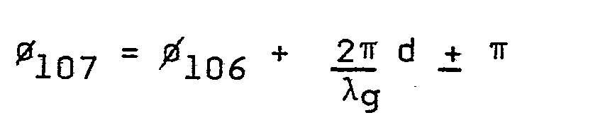
- As shown by the formula, the phase of slot 107 (Ø107) as compared to the phase of slot 106 (Ø106) is dependent upon the spacing d and the waveguide wavelength (λg). All other adjacent slots have similar phase relationships. Since spacing d is temperature dependent (conductive material such as copper or aluminum expands or contracts with temperature variations) and the waveguide wavelength x9 is frequency dependent,
travelling wave manifold 100 is both frequency and temperature dependent. - The monitored beam pointing angle, 0, for the travelling wave manifold having slots of alternating phase is defined as the pointing angle of a beam provided at the manifold output connector as a result of excitations imparted at the manifold slots. By reciprocity, it may be defined as the conjugate of the pointing angle of a beam radiated by the manifold output slots as a result of excitations imparted by the manifold input connector. The monitored beam pointing angle is given by:

- λo = reference free space wavelength (design center)
- λco = waveguide cutoff wavelength
- f = reference frequency o
- f = frequency of excitations
- This equation gives the explicit relationship between the monitored beam pointing angle, frequency and coupling slot spacing. The invention relates to: (a) microwave landing systems which use wide scanning phased array antenna systems having a sharp cutoff of the element pattern, such as are disclosed by Richard F. Frazita, Alfred R. Lopez and Richard J. Giannini in U.S. Patent No. 4,041,501; and (b) calibration of a system having plural signal carrying channels.
- Referring to Figure 2, generally such antenna systems include one or more radiating elements forming an array 1 in which the elements are arranged along an array axis and are spaced from each other by a given distance. Each of the elements is coupled to a power divider 8 via a corresponding one of a plurality of phase shifters 9 connected to the elements by
distribution network 2. Wave energy signals from signal generator 11 and power divider 8 are supplied to antenna elements 1 by phase shifters 9 such that a proper selection of the relative phase values for phase shifters 9 causes antenna elements. 12 to radiate a desired radiation pattern into a selected angular region of space. Variation of the relative phase values of the phase shifters 9 is accomplished bybeam steering unit 10 viacontrol line 22 and causes the radiated antenna pattern to change direction with respect to angle A in space. Therefore, phase shifters 9 andbeam steering unit 10 together form means 2 for scanning a beam radiated by the antenna elements of array 1 as a result of the supplied wave energy signals from generator 11 coupled to the elements of array 1 by power divider 8 anddistribution network 2. - The properties of a scanning antenna and techniques for selecting design parameters such as aperture length, element spacing and the particular configuration of the
distribution network 2 are well known in the prior art. A review of these parameters is completely described in U.S. Patent No. 4,041,501. - In order to stabilize the beam pointing angle of the radiated beam, an
aperture manifold 4 is associated with the antenna elements of array 1. Manifold 4 may be any means for forming a signal provided byoutput 12 which represents a beam pointing angle of the radiated beam. Preferably,manifold 4 is a highly phase stable waveguide or manifold, such as the invention, coupled to thearray 2 and center-fed to avoid inherent frequency (phase) and temperature effects. Center feeding also eliminates first-order dependence on frequency and absolute temperature variations. - As used herein,
manifold 4 refers to any type of device for sampling signals including a waveguide, a printed circuit network, a coaxial line network or a power combiner. A phase stable manifold is, by definition, one in which the beam formed by summing of the slot excitations is insensitive to frequency and temperature changes and is used in combination with a phased arrray in accordance with this invention to detect bias error at a specific angle. Manifold 4 is equivalent in function to a probe located in space at a specific angle with respect to the phased array. A manifold in accordance with the present invention may be a slotted waveguide configured to monitor radiated energy such that there is equal, non-zero phase and equal amplitude at all sample points (i.e. slot locations) of the manifold. - The
output 12 ofmanifold 4 is coupled to means 5, associated withmeans 3, for controlling the scanning of the radiated beam in response to theoutput 12 ofmanifold 4. - Figure 3 illustrates a
resonant waveguide 200 according to the invention.Waveguide 200 is provided with afirst end 201 terminating in a short circuit such as a conductive sheet of metal perpendicular to the sides ofwaveguide 200 and asecond end 202 terminating in a short circuit.Waveguide 200 is center fed by a transducer which converts an electrical signal into electromagnetic energy and vice versa. Preferably, the transducer is any connector well known in the prior art such asoutput connector 203 which receive waves propagating in both directions alongpath 204.Side 205 ofwaveguide 200 is provided withslots waveguide 200. - As shown by Figure 7, an incident wave radiated by
connector 203 has a constant amplitude Ainc along the entire length ofwaveguide 200. This is because amplitude tapers in the travelling wave caused by the coupling slots is counteracted and eliminated by the resonance ofwaveguide 200. - Due to reciprocity,
waveguide 200 may be used in either a transmitting or receiving mode. In the transmitting mode,connector 203 is connected viaisolator 215 to a signal source (not shown). The signal is converted byconnector 203 to electromagnetic wave energy which propagates alongwaveguide 200 and is radiated by slots 206-214. In the receiving mode, slots 206-214 are illuminated by electromagnetic wave energy which propagates alongwaveguide 200 and is converted byconnector 203 into an electrical signal. For convenience and according to convention, the invention has been described in a receiving mode. However, this disclosure and the scope of the claims appended hereto should not be limited to any one mode and should be broadly construed to include both transmitting and/or receiving operations. - Figure 8 is an illustration of the incident phase Øinc of the wave radiated by
connector 203 and illustrates that the phase alongwaveguide 200 is linearly changing. - Since
short circuits waveguide 200, figure 9 illustrates that the amplitude of the reflected wave Aref is constant along the entire length ofwaveguide 200. Similarly, the phase of the reflected wave Øref propagating withinwaveguide 200 is linearly changing with distance. The result, as illustrated in figure 11, is a standing wave having a plurality of cells of alternating phase of zero degrees and 180 degrees between spacing d of the slots. - As shown in Figure 4A, each slot is located within one of the standing wave cells of
waveguide 200 so that the resulting manifold output will be temperature and frequency independent as long as the variations in temperature and frequency are within the range such that there is one and only one slot or group of slots located within each standing wave cell. By alternating the direction and thereby the phase of adjacent slots, the resulting manifold output will provide equal phasing to all radiating elements. This aperture manifold provides a beam forming capability which is independent of frequency and temperature since the phase within each standing wave cell is constant. To prevent transmission of the reflected wave back throughconnector 203,isolator 215 is located within theline feeding connector 203. - As shown in Figure 4B, each slot is located within one of the standing wave cells of
waveguide 200. By alternating the direction and thereby the phase of the slots, the resulting manifold output will have equal phase for each coupling slot and will be temperature and frequency independent as long as the variations in temperature and frequency are within the range such that there is one and only one slot or group of slots located within each standing wave cell. By alternating the direction and thereby the phase of each group A, B, C and D of slots (N=2) and by alternating direction and thereby the phase of adjacent slots within each group, the resulting manifold output will approximate an 11.25 beam pointing angle. This aperture manifold provides a beam forming capability which is independent of frequency and temperature since the phase within each standing wave cell is constant. To prevent transmission of the reflected wave back throughconnector 203,isolator 215 is located within theline feeding connector 203. - The monitored beam pointing angle, 0, for
resonant manifold 200 according to the invention, over the operational frequency bandwidth, is given by:
manifold 200 is independent of frequency and coupling slot spacing over the operational frequency bandwidth. In the embodiment illustrated in Figure 4A, 8 = Oο(m = ∞) and the beam radiated is perpendicular topath 204. In the embodiment illustrated in Figure 4B, the beam pointing angle is generally not 0° and the beam radiated bymanifold 200 is not perpendicular topath 204 because of the nonequal phasing of the groups of slots. For example, an MLS ground system having a center operating frequency of 5.06GHz (i.e. À = 2.33 inches) and a group spacing (dg) of 5.97" would have a monitored beam pointing angle of 11.25°. - However, slots 206-214 may be phased to approximate any beam pointing angle desired. The range of the actual beam pointing angles which the slots of a particular manifold may approximate are limited by the physical configuration of the particular manifold. In any case, therefore, the phasing of
manifold 200 is independent of frequency and coupling slot spacing over the operational frequency bandwidth. - In order to achieve the results described above,
input connector 205 is initially matched towaveguide 200 as if each end ofwaveguide 200 terminated in a non-reflecting absorber as shown in the prior art illustrated in figure 1. Such a matchedconnector 205 is employed withwaveguide 200 terminating in short circuits as illustrated in figure 2 thereby resulting in the resonant standing wave as shown in figure 9. - To. achieve the in-phase condition of the adjacent coupling slots of
waveguide 200, the required waveguide wavelength λg is twice the spacing d between coupling slots 206-214. This spacing d is determined by the radiating characteristics of the phased array antenna associated withwaveguide 200 and is typically slightly larger than 1/2 wavelength. For the Microwave Landing System elevation phased array antenna, ridge loading as shown in Figure 6 is used to obtain this result. In particular, opposingridges waveguide 200R for eliminating odd mode resonance which may disturb the amplitude and phase of the slot excitations. - The maximum length, L, of a manifold according to the invention is limited by the operational frequency bandwidth of the phased array antenna with which it is associated. To limit the beam distortions caused by amplitude taper at the band edges, length L'should not exceed the value given below:


- Figure 12 illustrates
waveguide 200R in association withwaveguide 300 such as descibed by U.S. Patent No. 3,903,524, owned by Hazeltine Corporation.Waveguide 300 may be one of a series of parallel waveguides forming the azimuth antenna of a Microwave Landing System (MLS) ground system. Such a ground system requires monitoring to evaluate its performance. In order to provide such monitoring,waveguide 200R functions as a manifold and is associated with each of theparallel waveguides 300. Ridge loading inwaveguide 200R in the form ofridges waveguide 200 to the required spacing of radiatingwaveguides 300. Specifically,waveguide 300 with polarized radiatingslots 301 has anon-polarized opening 302 coupled to slot 208R. Other vertical waveguides would be coupled toslots - Figure 13 illustrates another MLS ground system coupling configuration having
non-polarized holes broad wall 509R ofwaveguide 500R and having ridge 510R on broad wall 511R. The non-polarized holes are coupled to_ parallel radiating waveguides such aswaveguide 300 bypolarized slot 303. For this configuration the required 180 degree phase reversals between adjacent coupling holes is incorporated in the design ofwaveguide 300.Adjacent waveguides 300 have a 180° phase reversal at their input wave launchers i.e.slot 303. - Figure 14 illustrates another MLS ground system coupling configuration wherein
slots dipole array 400 which may function as an MLS elevation antenna. Although this invention has been particularly described with regard to its function as an elevation manifold, it may be used as an azimuth manifold or ether array monitor.
Claims (13)
Applications Claiming Priority (4)
| Application Number | Priority Date | Filing Date | Title |
|---|---|---|---|
| US06/497,349 US4554550A (en) | 1983-05-23 | 1983-05-23 | Resonant waveguide aperture manifold |
| US06/497,350 US4554551A (en) | 1983-05-23 | 1983-05-23 | Asymmetric resonant waveguide aperture manifold |
| US497349 | 1995-06-30 | ||
| US497350 | 1995-06-30 |
Publications (3)
| Publication Number | Publication Date |
|---|---|
| EP0126626A2 true EP0126626A2 (en) | 1984-11-28 |
| EP0126626A3 EP0126626A3 (en) | 1987-02-04 |
| EP0126626B1 EP0126626B1 (en) | 1993-06-16 |
Family
ID=27052466
Family Applications (1)
| Application Number | Title | Priority Date | Filing Date |
|---|---|---|---|
| EP19840303356 Expired - Lifetime EP0126626B1 (en) | 1983-05-23 | 1984-05-17 | Resonant waveguide aperture manifold |
Country Status (4)
| Country | Link |
|---|---|
| EP (1) | EP0126626B1 (en) |
| AU (1) | AU565039B2 (en) |
| DE (1) | DE3486164T2 (en) |
| NZ (1) | NZ208213A (en) |
Cited By (9)
| Publication number | Priority date | Publication date | Assignee | Title |
|---|---|---|---|---|
| US4788552A (en) * | 1985-10-31 | 1988-11-29 | Telefonaktiebolaget L M Ericsson | Wave guide element for an electrically controlled radar antenna |
| EP0547274A1 (en) * | 1989-02-23 | 1993-06-23 | Hazeltine Corporation | Calibration of plural - channel system |
| EP0584635A1 (en) * | 1992-08-22 | 1994-03-02 | Alcatel SEL Aktiengesellschaft | Device for obtaining the aperture configuration of a phased array antenna |
| WO1996030963A1 (en) * | 1995-03-27 | 1996-10-03 | Hollandse Signaalapparaten B.V. | Phased array antenna provided with a calibration network |
| US5638079A (en) * | 1993-11-12 | 1997-06-10 | Ramot University Authority For Applied Research & Industrial Development Ltd. | Slotted waveguide array antennas |
| WO2002075840A2 (en) * | 2001-03-16 | 2002-09-26 | Marconi Intellectual Property (Us) Inc | Communicating with stackable objects using an antenna array |
| US7372418B2 (en) | 2002-04-24 | 2008-05-13 | Mineral Lassen Llc | Energy source communication employing slot antenna |
| RU2449435C1 (en) * | 2011-02-07 | 2012-04-27 | Государственное образовательное учреждение высшего профессионального образования Новгородский государственный университет имени Ярослава Мудрого | Flat array of diffraction radiation antennas and power divider used in it |
| CN111740198A (en) * | 2020-07-28 | 2020-10-02 | 成都玖信科技有限公司 | Ultra-wideband radial synthesizer |
Families Citing this family (161)
| Publication number | Priority date | Publication date | Assignee | Title |
|---|---|---|---|---|
| US9225048B2 (en) | 2011-02-23 | 2015-12-29 | General Electric Company | Antenna protection device and system |
| US10009065B2 (en) | 2012-12-05 | 2018-06-26 | At&T Intellectual Property I, L.P. | Backhaul link for distributed antenna system |
| US9113347B2 (en) | 2012-12-05 | 2015-08-18 | At&T Intellectual Property I, Lp | Backhaul link for distributed antenna system |
| US9525524B2 (en) | 2013-05-31 | 2016-12-20 | At&T Intellectual Property I, L.P. | Remote distributed antenna system |
| US9999038B2 (en) | 2013-05-31 | 2018-06-12 | At&T Intellectual Property I, L.P. | Remote distributed antenna system |
| US8897697B1 (en) | 2013-11-06 | 2014-11-25 | At&T Intellectual Property I, Lp | Millimeter-wave surface-wave communications |
| US9209902B2 (en) | 2013-12-10 | 2015-12-08 | At&T Intellectual Property I, L.P. | Quasi-optical coupler |
| US9692101B2 (en) | 2014-08-26 | 2017-06-27 | At&T Intellectual Property I, L.P. | Guided wave couplers for coupling electromagnetic waves between a waveguide surface and a surface of a wire |
| US9768833B2 (en) | 2014-09-15 | 2017-09-19 | At&T Intellectual Property I, L.P. | Method and apparatus for sensing a condition in a transmission medium of electromagnetic waves |
| US10063280B2 (en) | 2014-09-17 | 2018-08-28 | At&T Intellectual Property I, L.P. | Monitoring and mitigating conditions in a communication network |
| US9628854B2 (en) | 2014-09-29 | 2017-04-18 | At&T Intellectual Property I, L.P. | Method and apparatus for distributing content in a communication network |
| US9615269B2 (en) | 2014-10-02 | 2017-04-04 | At&T Intellectual Property I, L.P. | Method and apparatus that provides fault tolerance in a communication network |
| US9685992B2 (en) | 2014-10-03 | 2017-06-20 | At&T Intellectual Property I, L.P. | Circuit panel network and methods thereof |
| US9503189B2 (en) | 2014-10-10 | 2016-11-22 | At&T Intellectual Property I, L.P. | Method and apparatus for arranging communication sessions in a communication system |
| US9973299B2 (en) | 2014-10-14 | 2018-05-15 | At&T Intellectual Property I, L.P. | Method and apparatus for adjusting a mode of communication in a communication network |
| US9762289B2 (en) | 2014-10-14 | 2017-09-12 | At&T Intellectual Property I, L.P. | Method and apparatus for transmitting or receiving signals in a transportation system |
| US9627768B2 (en) | 2014-10-21 | 2017-04-18 | At&T Intellectual Property I, L.P. | Guided-wave transmission device with non-fundamental mode propagation and methods for use therewith |
| US9653770B2 (en) | 2014-10-21 | 2017-05-16 | At&T Intellectual Property I, L.P. | Guided wave coupler, coupling module and methods for use therewith |
| US9769020B2 (en) | 2014-10-21 | 2017-09-19 | At&T Intellectual Property I, L.P. | Method and apparatus for responding to events affecting communications in a communication network |
| US9577306B2 (en) | 2014-10-21 | 2017-02-21 | At&T Intellectual Property I, L.P. | Guided-wave transmission device and methods for use therewith |
| US9520945B2 (en) | 2014-10-21 | 2016-12-13 | At&T Intellectual Property I, L.P. | Apparatus for providing communication services and methods thereof |
| US9780834B2 (en) | 2014-10-21 | 2017-10-03 | At&T Intellectual Property I, L.P. | Method and apparatus for transmitting electromagnetic waves |
| US9564947B2 (en) | 2014-10-21 | 2017-02-07 | At&T Intellectual Property I, L.P. | Guided-wave transmission device with diversity and methods for use therewith |
| US9312919B1 (en) | 2014-10-21 | 2016-04-12 | At&T Intellectual Property I, Lp | Transmission device with impairment compensation and methods for use therewith |
| US9461706B1 (en) | 2015-07-31 | 2016-10-04 | At&T Intellectual Property I, Lp | Method and apparatus for exchanging communication signals |
| US10340573B2 (en) | 2016-10-26 | 2019-07-02 | At&T Intellectual Property I, L.P. | Launcher with cylindrical coupling device and methods for use therewith |
| US9800327B2 (en) | 2014-11-20 | 2017-10-24 | At&T Intellectual Property I, L.P. | Apparatus for controlling operations of a communication device and methods thereof |
| US9954287B2 (en) | 2014-11-20 | 2018-04-24 | At&T Intellectual Property I, L.P. | Apparatus for converting wireless signals and electromagnetic waves and methods thereof |
| US9680670B2 (en) | 2014-11-20 | 2017-06-13 | At&T Intellectual Property I, L.P. | Transmission device with channel equalization and control and methods for use therewith |
| US9742462B2 (en) | 2014-12-04 | 2017-08-22 | At&T Intellectual Property I, L.P. | Transmission medium and communication interfaces and methods for use therewith |
| US9997819B2 (en) | 2015-06-09 | 2018-06-12 | At&T Intellectual Property I, L.P. | Transmission medium and method for facilitating propagation of electromagnetic waves via a core |
| US9544006B2 (en) | 2014-11-20 | 2017-01-10 | At&T Intellectual Property I, L.P. | Transmission device with mode division multiplexing and methods for use therewith |
| US10009067B2 (en) | 2014-12-04 | 2018-06-26 | At&T Intellectual Property I, L.P. | Method and apparatus for configuring a communication interface |
| US10243784B2 (en) | 2014-11-20 | 2019-03-26 | At&T Intellectual Property I, L.P. | System for generating topology information and methods thereof |
| US9654173B2 (en) | 2014-11-20 | 2017-05-16 | At&T Intellectual Property I, L.P. | Apparatus for powering a communication device and methods thereof |
| US10144036B2 (en) | 2015-01-30 | 2018-12-04 | At&T Intellectual Property I, L.P. | Method and apparatus for mitigating interference affecting a propagation of electromagnetic waves guided by a transmission medium |
| US9876570B2 (en) | 2015-02-20 | 2018-01-23 | At&T Intellectual Property I, Lp | Guided-wave transmission device with non-fundamental mode propagation and methods for use therewith |
| US9749013B2 (en) | 2015-03-17 | 2017-08-29 | At&T Intellectual Property I, L.P. | Method and apparatus for reducing attenuation of electromagnetic waves guided by a transmission medium |
| US9705561B2 (en) | 2015-04-24 | 2017-07-11 | At&T Intellectual Property I, L.P. | Directional coupling device and methods for use therewith |
| US10224981B2 (en) | 2015-04-24 | 2019-03-05 | At&T Intellectual Property I, Lp | Passive electrical coupling device and methods for use therewith |
| US9793954B2 (en) | 2015-04-28 | 2017-10-17 | At&T Intellectual Property I, L.P. | Magnetic coupling device and methods for use therewith |
| US9948354B2 (en) | 2015-04-28 | 2018-04-17 | At&T Intellectual Property I, L.P. | Magnetic coupling device with reflective plate and methods for use therewith |
| US9871282B2 (en) | 2015-05-14 | 2018-01-16 | At&T Intellectual Property I, L.P. | At least one transmission medium having a dielectric surface that is covered at least in part by a second dielectric |
| US9490869B1 (en) | 2015-05-14 | 2016-11-08 | At&T Intellectual Property I, L.P. | Transmission medium having multiple cores and methods for use therewith |
| US9748626B2 (en) | 2015-05-14 | 2017-08-29 | At&T Intellectual Property I, L.P. | Plurality of cables having different cross-sectional shapes which are bundled together to form a transmission medium |
| US10679767B2 (en) | 2015-05-15 | 2020-06-09 | At&T Intellectual Property I, L.P. | Transmission medium having a conductive material and methods for use therewith |
| US10650940B2 (en) | 2015-05-15 | 2020-05-12 | At&T Intellectual Property I, L.P. | Transmission medium having a conductive material and methods for use therewith |
| US9917341B2 (en) | 2015-05-27 | 2018-03-13 | At&T Intellectual Property I, L.P. | Apparatus and method for launching electromagnetic waves and for modifying radial dimensions of the propagating electromagnetic waves |
| US10348391B2 (en) | 2015-06-03 | 2019-07-09 | At&T Intellectual Property I, L.P. | Client node device with frequency conversion and methods for use therewith |
| US10103801B2 (en) | 2015-06-03 | 2018-10-16 | At&T Intellectual Property I, L.P. | Host node device and methods for use therewith |
| US9866309B2 (en) | 2015-06-03 | 2018-01-09 | At&T Intellectual Property I, Lp | Host node device and methods for use therewith |
| US10812174B2 (en) | 2015-06-03 | 2020-10-20 | At&T Intellectual Property I, L.P. | Client node device and methods for use therewith |
| US10154493B2 (en) | 2015-06-03 | 2018-12-11 | At&T Intellectual Property I, L.P. | Network termination and methods for use therewith |
| US9912381B2 (en) | 2015-06-03 | 2018-03-06 | At&T Intellectual Property I, Lp | Network termination and methods for use therewith |
| US9913139B2 (en) | 2015-06-09 | 2018-03-06 | At&T Intellectual Property I, L.P. | Signal fingerprinting for authentication of communicating devices |
| US10142086B2 (en) | 2015-06-11 | 2018-11-27 | At&T Intellectual Property I, L.P. | Repeater and methods for use therewith |
| US9608692B2 (en) | 2015-06-11 | 2017-03-28 | At&T Intellectual Property I, L.P. | Repeater and methods for use therewith |
| US9820146B2 (en) | 2015-06-12 | 2017-11-14 | At&T Intellectual Property I, L.P. | Method and apparatus for authentication and identity management of communicating devices |
| US9667317B2 (en) | 2015-06-15 | 2017-05-30 | At&T Intellectual Property I, L.P. | Method and apparatus for providing security using network traffic adjustments |
| US9865911B2 (en) | 2015-06-25 | 2018-01-09 | At&T Intellectual Property I, L.P. | Waveguide system for slot radiating first electromagnetic waves that are combined into a non-fundamental wave mode second electromagnetic wave on a transmission medium |
| US9640850B2 (en) | 2015-06-25 | 2017-05-02 | At&T Intellectual Property I, L.P. | Methods and apparatus for inducing a non-fundamental wave mode on a transmission medium |
| US9509415B1 (en) | 2015-06-25 | 2016-11-29 | At&T Intellectual Property I, L.P. | Methods and apparatus for inducing a fundamental wave mode on a transmission medium |
| US9853342B2 (en) | 2015-07-14 | 2017-12-26 | At&T Intellectual Property I, L.P. | Dielectric transmission medium connector and methods for use therewith |
| US9882257B2 (en) | 2015-07-14 | 2018-01-30 | At&T Intellectual Property I, L.P. | Method and apparatus for launching a wave mode that mitigates interference |
| US9836957B2 (en) | 2015-07-14 | 2017-12-05 | At&T Intellectual Property I, L.P. | Method and apparatus for communicating with premises equipment |
| US10341142B2 (en) | 2015-07-14 | 2019-07-02 | At&T Intellectual Property I, L.P. | Apparatus and methods for generating non-interfering electromagnetic waves on an uninsulated conductor |
| US10320586B2 (en) | 2015-07-14 | 2019-06-11 | At&T Intellectual Property I, L.P. | Apparatus and methods for generating non-interfering electromagnetic waves on an insulated transmission medium |
| US10033108B2 (en) | 2015-07-14 | 2018-07-24 | At&T Intellectual Property I, L.P. | Apparatus and methods for generating an electromagnetic wave having a wave mode that mitigates interference |
| US10205655B2 (en) | 2015-07-14 | 2019-02-12 | At&T Intellectual Property I, L.P. | Apparatus and methods for communicating utilizing an antenna array and multiple communication paths |
| US9722318B2 (en) | 2015-07-14 | 2017-08-01 | At&T Intellectual Property I, L.P. | Method and apparatus for coupling an antenna to a device |
| US10033107B2 (en) | 2015-07-14 | 2018-07-24 | At&T Intellectual Property I, L.P. | Method and apparatus for coupling an antenna to a device |
| US9628116B2 (en) | 2015-07-14 | 2017-04-18 | At&T Intellectual Property I, L.P. | Apparatus and methods for transmitting wireless signals |
| US9847566B2 (en) | 2015-07-14 | 2017-12-19 | At&T Intellectual Property I, L.P. | Method and apparatus for adjusting a field of a signal to mitigate interference |
| US10044409B2 (en) | 2015-07-14 | 2018-08-07 | At&T Intellectual Property I, L.P. | Transmission medium and methods for use therewith |
| US10148016B2 (en) | 2015-07-14 | 2018-12-04 | At&T Intellectual Property I, L.P. | Apparatus and methods for communicating utilizing an antenna array |
| US10170840B2 (en) | 2015-07-14 | 2019-01-01 | At&T Intellectual Property I, L.P. | Apparatus and methods for sending or receiving electromagnetic signals |
| US9793951B2 (en) | 2015-07-15 | 2017-10-17 | At&T Intellectual Property I, L.P. | Method and apparatus for launching a wave mode that mitigates interference |
| US9608740B2 (en) | 2015-07-15 | 2017-03-28 | At&T Intellectual Property I, L.P. | Method and apparatus for launching a wave mode that mitigates interference |
| US10090606B2 (en) | 2015-07-15 | 2018-10-02 | At&T Intellectual Property I, L.P. | Antenna system with dielectric array and methods for use therewith |
| US9912027B2 (en) | 2015-07-23 | 2018-03-06 | At&T Intellectual Property I, L.P. | Method and apparatus for exchanging communication signals |
| US9871283B2 (en) | 2015-07-23 | 2018-01-16 | At&T Intellectual Property I, Lp | Transmission medium having a dielectric core comprised of plural members connected by a ball and socket configuration |
| US9749053B2 (en) | 2015-07-23 | 2017-08-29 | At&T Intellectual Property I, L.P. | Node device, repeater and methods for use therewith |
| US10784670B2 (en) | 2015-07-23 | 2020-09-22 | At&T Intellectual Property I, L.P. | Antenna support for aligning an antenna |
| US9948333B2 (en) | 2015-07-23 | 2018-04-17 | At&T Intellectual Property I, L.P. | Method and apparatus for wireless communications to mitigate interference |
| US9967173B2 (en) | 2015-07-31 | 2018-05-08 | At&T Intellectual Property I, L.P. | Method and apparatus for authentication and identity management of communicating devices |
| US10020587B2 (en) | 2015-07-31 | 2018-07-10 | At&T Intellectual Property I, L.P. | Radial antenna and methods for use therewith |
| US9735833B2 (en) | 2015-07-31 | 2017-08-15 | At&T Intellectual Property I, L.P. | Method and apparatus for communications management in a neighborhood network |
| US9904535B2 (en) | 2015-09-14 | 2018-02-27 | At&T Intellectual Property I, L.P. | Method and apparatus for distributing software |
| US10051629B2 (en) | 2015-09-16 | 2018-08-14 | At&T Intellectual Property I, L.P. | Method and apparatus for use with a radio distributed antenna system having an in-band reference signal |
| US10136434B2 (en) | 2015-09-16 | 2018-11-20 | At&T Intellectual Property I, L.P. | Method and apparatus for use with a radio distributed antenna system having an ultra-wideband control channel |
| US10009063B2 (en) | 2015-09-16 | 2018-06-26 | At&T Intellectual Property I, L.P. | Method and apparatus for use with a radio distributed antenna system having an out-of-band reference signal |
| US10079661B2 (en) | 2015-09-16 | 2018-09-18 | At&T Intellectual Property I, L.P. | Method and apparatus for use with a radio distributed antenna system having a clock reference |
| US10009901B2 (en) | 2015-09-16 | 2018-06-26 | At&T Intellectual Property I, L.P. | Method, apparatus, and computer-readable storage medium for managing utilization of wireless resources between base stations |
| US9769128B2 (en) | 2015-09-28 | 2017-09-19 | At&T Intellectual Property I, L.P. | Method and apparatus for encryption of communications over a network |
| US9729197B2 (en) | 2015-10-01 | 2017-08-08 | At&T Intellectual Property I, L.P. | Method and apparatus for communicating network management traffic over a network |
| US9876264B2 (en) | 2015-10-02 | 2018-01-23 | At&T Intellectual Property I, Lp | Communication system, guided wave switch and methods for use therewith |
| US9882277B2 (en) | 2015-10-02 | 2018-01-30 | At&T Intellectual Property I, Lp | Communication device and antenna assembly with actuated gimbal mount |
| US10074890B2 (en) | 2015-10-02 | 2018-09-11 | At&T Intellectual Property I, L.P. | Communication device and antenna with integrated light assembly |
| US10355367B2 (en) | 2015-10-16 | 2019-07-16 | At&T Intellectual Property I, L.P. | Antenna structure for exchanging wireless signals |
| US10051483B2 (en) | 2015-10-16 | 2018-08-14 | At&T Intellectual Property I, L.P. | Method and apparatus for directing wireless signals |
| US10665942B2 (en) | 2015-10-16 | 2020-05-26 | At&T Intellectual Property I, L.P. | Method and apparatus for adjusting wireless communications |
| US9912419B1 (en) | 2016-08-24 | 2018-03-06 | At&T Intellectual Property I, L.P. | Method and apparatus for managing a fault in a distributed antenna system |
| US9860075B1 (en) | 2016-08-26 | 2018-01-02 | At&T Intellectual Property I, L.P. | Method and communication node for broadband distribution |
| US10291311B2 (en) | 2016-09-09 | 2019-05-14 | At&T Intellectual Property I, L.P. | Method and apparatus for mitigating a fault in a distributed antenna system |
| US11032819B2 (en) | 2016-09-15 | 2021-06-08 | At&T Intellectual Property I, L.P. | Method and apparatus for use with a radio distributed antenna system having a control channel reference signal |
| US10135146B2 (en) | 2016-10-18 | 2018-11-20 | At&T Intellectual Property I, L.P. | Apparatus and methods for launching guided waves via circuits |
| US10135147B2 (en) | 2016-10-18 | 2018-11-20 | At&T Intellectual Property I, L.P. | Apparatus and methods for launching guided waves via an antenna |
| US10340600B2 (en) | 2016-10-18 | 2019-07-02 | At&T Intellectual Property I, L.P. | Apparatus and methods for launching guided waves via plural waveguide systems |
| US9991580B2 (en) | 2016-10-21 | 2018-06-05 | At&T Intellectual Property I, L.P. | Launcher and coupling system for guided wave mode cancellation |
| US10811767B2 (en) | 2016-10-21 | 2020-10-20 | At&T Intellectual Property I, L.P. | System and dielectric antenna with convex dielectric radome |
| US9876605B1 (en) | 2016-10-21 | 2018-01-23 | At&T Intellectual Property I, L.P. | Launcher and coupling system to support desired guided wave mode |
| US10374316B2 (en) | 2016-10-21 | 2019-08-06 | At&T Intellectual Property I, L.P. | System and dielectric antenna with non-uniform dielectric |
| US10312567B2 (en) | 2016-10-26 | 2019-06-04 | At&T Intellectual Property I, L.P. | Launcher with planar strip antenna and methods for use therewith |
| US10225025B2 (en) | 2016-11-03 | 2019-03-05 | At&T Intellectual Property I, L.P. | Method and apparatus for detecting a fault in a communication system |
| US10498044B2 (en) | 2016-11-03 | 2019-12-03 | At&T Intellectual Property I, L.P. | Apparatus for configuring a surface of an antenna |
| US10224634B2 (en) | 2016-11-03 | 2019-03-05 | At&T Intellectual Property I, L.P. | Methods and apparatus for adjusting an operational characteristic of an antenna |
| US10291334B2 (en) | 2016-11-03 | 2019-05-14 | At&T Intellectual Property I, L.P. | System for detecting a fault in a communication system |
| US10178445B2 (en) | 2016-11-23 | 2019-01-08 | At&T Intellectual Property I, L.P. | Methods, devices, and systems for load balancing between a plurality of waveguides |
| US10340603B2 (en) | 2016-11-23 | 2019-07-02 | At&T Intellectual Property I, L.P. | Antenna system having shielded structural configurations for assembly |
| US10535928B2 (en) | 2016-11-23 | 2020-01-14 | At&T Intellectual Property I, L.P. | Antenna system and methods for use therewith |
| US10090594B2 (en) | 2016-11-23 | 2018-10-02 | At&T Intellectual Property I, L.P. | Antenna system having structural configurations for assembly |
| US10340601B2 (en) | 2016-11-23 | 2019-07-02 | At&T Intellectual Property I, L.P. | Multi-antenna system and methods for use therewith |
| US10361489B2 (en) | 2016-12-01 | 2019-07-23 | At&T Intellectual Property I, L.P. | Dielectric dish antenna system and methods for use therewith |
| US10305190B2 (en) | 2016-12-01 | 2019-05-28 | At&T Intellectual Property I, L.P. | Reflecting dielectric antenna system and methods for use therewith |
| US9927517B1 (en) | 2016-12-06 | 2018-03-27 | At&T Intellectual Property I, L.P. | Apparatus and methods for sensing rainfall |
| US10439675B2 (en) | 2016-12-06 | 2019-10-08 | At&T Intellectual Property I, L.P. | Method and apparatus for repeating guided wave communication signals |
| US10727599B2 (en) | 2016-12-06 | 2020-07-28 | At&T Intellectual Property I, L.P. | Launcher with slot antenna and methods for use therewith |
| US10694379B2 (en) | 2016-12-06 | 2020-06-23 | At&T Intellectual Property I, L.P. | Waveguide system with device-based authentication and methods for use therewith |
| US10326494B2 (en) | 2016-12-06 | 2019-06-18 | At&T Intellectual Property I, L.P. | Apparatus for measurement de-embedding and methods for use therewith |
| US10020844B2 (en) | 2016-12-06 | 2018-07-10 | T&T Intellectual Property I, L.P. | Method and apparatus for broadcast communication via guided waves |
| US10755542B2 (en) | 2016-12-06 | 2020-08-25 | At&T Intellectual Property I, L.P. | Method and apparatus for surveillance via guided wave communication |
| US10135145B2 (en) | 2016-12-06 | 2018-11-20 | At&T Intellectual Property I, L.P. | Apparatus and methods for generating an electromagnetic wave along a transmission medium |
| US10819035B2 (en) | 2016-12-06 | 2020-10-27 | At&T Intellectual Property I, L.P. | Launcher with helical antenna and methods for use therewith |
| US10382976B2 (en) | 2016-12-06 | 2019-08-13 | At&T Intellectual Property I, L.P. | Method and apparatus for managing wireless communications based on communication paths and network device positions |
| US10637149B2 (en) | 2016-12-06 | 2020-04-28 | At&T Intellectual Property I, L.P. | Injection molded dielectric antenna and methods for use therewith |
| US10139820B2 (en) | 2016-12-07 | 2018-11-27 | At&T Intellectual Property I, L.P. | Method and apparatus for deploying equipment of a communication system |
| US10243270B2 (en) | 2016-12-07 | 2019-03-26 | At&T Intellectual Property I, L.P. | Beam adaptive multi-feed dielectric antenna system and methods for use therewith |
| US10168695B2 (en) | 2016-12-07 | 2019-01-01 | At&T Intellectual Property I, L.P. | Method and apparatus for controlling an unmanned aircraft |
| US10446936B2 (en) | 2016-12-07 | 2019-10-15 | At&T Intellectual Property I, L.P. | Multi-feed dielectric antenna system and methods for use therewith |
| US9893795B1 (en) | 2016-12-07 | 2018-02-13 | At&T Intellectual Property I, Lp | Method and repeater for broadband distribution |
| US10547348B2 (en) | 2016-12-07 | 2020-01-28 | At&T Intellectual Property I, L.P. | Method and apparatus for switching transmission mediums in a communication system |
| US10389029B2 (en) | 2016-12-07 | 2019-08-20 | At&T Intellectual Property I, L.P. | Multi-feed dielectric antenna system with core selection and methods for use therewith |
| US10359749B2 (en) | 2016-12-07 | 2019-07-23 | At&T Intellectual Property I, L.P. | Method and apparatus for utilities management via guided wave communication |
| US10027397B2 (en) | 2016-12-07 | 2018-07-17 | At&T Intellectual Property I, L.P. | Distributed antenna system and methods for use therewith |
| US10389037B2 (en) | 2016-12-08 | 2019-08-20 | At&T Intellectual Property I, L.P. | Apparatus and methods for selecting sections of an antenna array and use therewith |
| US10777873B2 (en) | 2016-12-08 | 2020-09-15 | At&T Intellectual Property I, L.P. | Method and apparatus for mounting network devices |
| US10411356B2 (en) | 2016-12-08 | 2019-09-10 | At&T Intellectual Property I, L.P. | Apparatus and methods for selectively targeting communication devices with an antenna array |
| US10601494B2 (en) | 2016-12-08 | 2020-03-24 | At&T Intellectual Property I, L.P. | Dual-band communication device and method for use therewith |
| US9911020B1 (en) | 2016-12-08 | 2018-03-06 | At&T Intellectual Property I, L.P. | Method and apparatus for tracking via a radio frequency identification device |
| US10326689B2 (en) | 2016-12-08 | 2019-06-18 | At&T Intellectual Property I, L.P. | Method and system for providing alternative communication paths |
| US10530505B2 (en) | 2016-12-08 | 2020-01-07 | At&T Intellectual Property I, L.P. | Apparatus and methods for launching electromagnetic waves along a transmission medium |
| US10103422B2 (en) | 2016-12-08 | 2018-10-16 | At&T Intellectual Property I, L.P. | Method and apparatus for mounting network devices |
| US10938108B2 (en) | 2016-12-08 | 2021-03-02 | At&T Intellectual Property I, L.P. | Frequency selective multi-feed dielectric antenna system and methods for use therewith |
| US10069535B2 (en) | 2016-12-08 | 2018-09-04 | At&T Intellectual Property I, L.P. | Apparatus and methods for launching electromagnetic waves having a certain electric field structure |
| US10916969B2 (en) | 2016-12-08 | 2021-02-09 | At&T Intellectual Property I, L.P. | Method and apparatus for providing power using an inductive coupling |
| US9998870B1 (en) | 2016-12-08 | 2018-06-12 | At&T Intellectual Property I, L.P. | Method and apparatus for proximity sensing |
| US10264586B2 (en) | 2016-12-09 | 2019-04-16 | At&T Mobility Ii Llc | Cloud-based packet controller and methods for use therewith |
| US10340983B2 (en) | 2016-12-09 | 2019-07-02 | At&T Intellectual Property I, L.P. | Method and apparatus for surveying remote sites via guided wave communications |
| US9838896B1 (en) | 2016-12-09 | 2017-12-05 | At&T Intellectual Property I, L.P. | Method and apparatus for assessing network coverage |
| US9973940B1 (en) | 2017-02-27 | 2018-05-15 | At&T Intellectual Property I, L.P. | Apparatus and methods for dynamic impedance matching of a guided wave launcher |
| US10298293B2 (en) | 2017-03-13 | 2019-05-21 | At&T Intellectual Property I, L.P. | Apparatus of communication utilizing wireless network devices |
Citations (5)
| Publication number | Priority date | Publication date | Assignee | Title |
|---|---|---|---|---|
| US2905940A (en) * | 1957-05-02 | 1959-09-22 | Edward G Spencer | Electromagnetically steered microwave antenna |
| US3293550A (en) * | 1963-07-23 | 1966-12-20 | Rca Corp | Transmit monitor |
| US3328800A (en) * | 1964-03-12 | 1967-06-27 | North American Aviation Inc | Slot antenna utilizing variable standing wave pattern for controlling slot excitation |
| AU508205B2 (en) * | 1975-12-24 | 1980-03-13 | Commonwealth Scientific And Industrial Research Organization | Monitoring scanning radio beams |
| EP0106438A1 (en) * | 1982-09-07 | 1984-04-25 | Hazeltine Corporation | Phased array antenna |
-
1984
- 1984-05-11 AU AU27924/84A patent/AU565039B2/en not_active Ceased
- 1984-05-17 EP EP19840303356 patent/EP0126626B1/en not_active Expired - Lifetime
- 1984-05-17 DE DE19843486164 patent/DE3486164T2/en not_active Expired - Fee Related
- 1984-05-18 NZ NZ20821384A patent/NZ208213A/en unknown
Patent Citations (5)
| Publication number | Priority date | Publication date | Assignee | Title |
|---|---|---|---|---|
| US2905940A (en) * | 1957-05-02 | 1959-09-22 | Edward G Spencer | Electromagnetically steered microwave antenna |
| US3293550A (en) * | 1963-07-23 | 1966-12-20 | Rca Corp | Transmit monitor |
| US3328800A (en) * | 1964-03-12 | 1967-06-27 | North American Aviation Inc | Slot antenna utilizing variable standing wave pattern for controlling slot excitation |
| AU508205B2 (en) * | 1975-12-24 | 1980-03-13 | Commonwealth Scientific And Industrial Research Organization | Monitoring scanning radio beams |
| EP0106438A1 (en) * | 1982-09-07 | 1984-04-25 | Hazeltine Corporation | Phased array antenna |
Non-Patent Citations (1)
| Title |
|---|
| TELECOMMUNICATIONS AND RADIO ENGINEERING, vol. 25/26, no. 10, October 1971, pages 50-55; P.A. MEL'YANOVSKIY et al.: "Methods for monitoring the parameters of phased antenna arrays" * |
Cited By (12)
| Publication number | Priority date | Publication date | Assignee | Title |
|---|---|---|---|---|
| US4788552A (en) * | 1985-10-31 | 1988-11-29 | Telefonaktiebolaget L M Ericsson | Wave guide element for an electrically controlled radar antenna |
| EP0547274A1 (en) * | 1989-02-23 | 1993-06-23 | Hazeltine Corporation | Calibration of plural - channel system |
| EP0584635A1 (en) * | 1992-08-22 | 1994-03-02 | Alcatel SEL Aktiengesellschaft | Device for obtaining the aperture configuration of a phased array antenna |
| US5638079A (en) * | 1993-11-12 | 1997-06-10 | Ramot University Authority For Applied Research & Industrial Development Ltd. | Slotted waveguide array antennas |
| WO1996030963A1 (en) * | 1995-03-27 | 1996-10-03 | Hollandse Signaalapparaten B.V. | Phased array antenna provided with a calibration network |
| NL9500580A (en) * | 1995-03-27 | 1996-11-01 | Hollandse Signaalapparaten Bv | Phased array antenna equipped with a calibration network. |
| WO2002075840A2 (en) * | 2001-03-16 | 2002-09-26 | Marconi Intellectual Property (Us) Inc | Communicating with stackable objects using an antenna array |
| WO2002075840A3 (en) * | 2001-03-16 | 2003-02-20 | Marconi Corp Plc | Communicating with stackable objects using an antenna array |
| US7372418B2 (en) | 2002-04-24 | 2008-05-13 | Mineral Lassen Llc | Energy source communication employing slot antenna |
| US7414589B2 (en) | 2002-04-24 | 2008-08-19 | Mineral Lassen Llc | Energy source communication employing slot antenna |
| RU2449435C1 (en) * | 2011-02-07 | 2012-04-27 | Государственное образовательное учреждение высшего профессионального образования Новгородский государственный университет имени Ярослава Мудрого | Flat array of diffraction radiation antennas and power divider used in it |
| CN111740198A (en) * | 2020-07-28 | 2020-10-02 | 成都玖信科技有限公司 | Ultra-wideband radial synthesizer |
Also Published As
| Publication number | Publication date |
|---|---|
| EP0126626B1 (en) | 1993-06-16 |
| AU565039B2 (en) | 1987-09-03 |
| NZ208213A (en) | 1987-10-30 |
| AU2792484A (en) | 1984-11-29 |
| EP0126626A3 (en) | 1987-02-04 |
| DE3486164T2 (en) | 1994-01-13 |
| DE3486164D1 (en) | 1993-07-22 |
Similar Documents
| Publication | Publication Date | Title |
|---|---|---|
| EP0126626B1 (en) | Resonant waveguide aperture manifold | |
| US4939527A (en) | Distribution network for phased array antennas | |
| Ehrenspeck et al. | A new method for obtaining maximum gain from Yagi antennas | |
| US9537212B2 (en) | Antenna array system for producing dual circular polarization signals utilizing a meandering waveguide | |
| JP2585399B2 (en) | Dual mode phased array antenna system | |
| US3305867A (en) | Antenna array system | |
| US4975712A (en) | Two-dimensional scanning antenna | |
| EP0390350B1 (en) | Low cross-polarization radiator of circularly polarized radiation | |
| KR0184529B1 (en) | Slot-coupled fed dual circular polarization tem mode slot array antenna | |
| US4187507A (en) | Multiple beam antenna array | |
| JPH0444441B2 (en) | ||
| EP0506838B1 (en) | Broadband circular phased array antenna | |
| US3977006A (en) | Compensated traveling wave slotted waveguide feed for cophasal arrays | |
| US4996535A (en) | Shortened dual-mode horn antenna | |
| GB1594988A (en) | Antenna coupling network with element pattern shift | |
| EP0427470B1 (en) | Constant beamwidth scanning array | |
| US4554551A (en) | Asymmetric resonant waveguide aperture manifold | |
| US6542130B2 (en) | Tuneable antenna | |
| US4554550A (en) | Resonant waveguide aperture manifold | |
| US6222492B1 (en) | Dual coaxial feed for tracking antenna | |
| US4590479A (en) | Broadcast antenna system with high power aural/visual self-diplexing capability | |
| JPH0287704A (en) | Angle diversity signal separator using mode conversion | |
| Chen | Wideband wide-angle impedance matching and polarization characteristics of circular waveguide phased arrays | |
| Solbach | Below-resonant-length slot radiators for traveling-wave-array antennas | |
| Rotman et al. | The sandwich wire antenna: A new type of microwave line source radiator |
Legal Events
| Date | Code | Title | Description |
|---|---|---|---|
| PUAI | Public reference made under article 153(3) epc to a published international application that has entered the european phase |
Free format text: ORIGINAL CODE: 0009012 |
|
| AK | Designated contracting states |
Kind code of ref document: A2 Designated state(s): DE FR GB IT NL SE Designated state(s): DE FR GB IT NL SE |
|
| PUAL | Search report despatched |
Free format text: ORIGINAL CODE: 0009013 |
|
| AK | Designated contracting states |
Kind code of ref document: A3 Designated state(s): DE FR GB IT NL SE |
|
| 17P | Request for examination filed |
Effective date: 19870730 |
|
| 17Q | First examination report despatched |
Effective date: 19890725 |
|
| RAP3 | Party data changed (applicant data changed or rights of an application transferred) |
Owner name: HAZELTINE CORPORATION |
|
| GRAA | (expected) grant |
Free format text: ORIGINAL CODE: 0009210 |
|
| AK | Designated contracting states |
Kind code of ref document: B1 Designated state(s): DE FR GB IT NL SE |
|
| ITF | It: translation for a ep patent filed |
Owner name: JACOBACCI CASETTA & PERANI S.P.A. |
|
| REF | Corresponds to: |
Ref document number: 3486164 Country of ref document: DE Date of ref document: 19930722 |
|
| ET | Fr: translation filed | ||
| PLBE | No opposition filed within time limit |
Free format text: ORIGINAL CODE: 0009261 |
|
| STAA | Information on the status of an ep patent application or granted ep patent |
Free format text: STATUS: NO OPPOSITION FILED WITHIN TIME LIMIT |
|
| PG25 | Lapsed in a contracting state [announced via postgrant information from national office to epo] |
Ref country code: SE Effective date: 19940518 |
|
| PGFP | Annual fee paid to national office [announced via postgrant information from national office to epo] |
Ref country code: NL Payment date: 19940531 Year of fee payment: 11 |
|
| 26N | No opposition filed | ||
| EUG | Se: european patent has lapsed |
Ref document number: 84303356.4 Effective date: 19941210 |
|
| EUG | Se: european patent has lapsed |
Ref document number: 84303356.4 |
|
| PG25 | Lapsed in a contracting state [announced via postgrant information from national office to epo] |
Ref country code: NL Effective date: 19951201 |
|
| NLV4 | Nl: lapsed or anulled due to non-payment of the annual fee |
Effective date: 19951201 |
|
| PGFP | Annual fee paid to national office [announced via postgrant information from national office to epo] |
Ref country code: FR Payment date: 19990318 Year of fee payment: 16 |
|
| PGFP | Annual fee paid to national office [announced via postgrant information from national office to epo] |
Ref country code: GB Payment date: 19990325 Year of fee payment: 16 |
|
| PGFP | Annual fee paid to national office [announced via postgrant information from national office to epo] |
Ref country code: DE Payment date: 19990603 Year of fee payment: 16 |
|
| PG25 | Lapsed in a contracting state [announced via postgrant information from national office to epo] |
Ref country code: GB Free format text: LAPSE BECAUSE OF NON-PAYMENT OF DUE FEES Effective date: 20000517 |
|
| GBPC | Gb: european patent ceased through non-payment of renewal fee |
Effective date: 20000517 |
|
| PG25 | Lapsed in a contracting state [announced via postgrant information from national office to epo] |
Ref country code: FR Free format text: LAPSE BECAUSE OF NON-PAYMENT OF DUE FEES Effective date: 20010131 |
|
| PG25 | Lapsed in a contracting state [announced via postgrant information from national office to epo] |
Ref country code: DE Free format text: LAPSE BECAUSE OF NON-PAYMENT OF DUE FEES Effective date: 20010301 |
|
| REG | Reference to a national code |
Ref country code: FR Ref legal event code: ST |